

Boron Nitride Thin Films with Anisotropic Optical Properties from Microscale Particle Density Distributions

 , , , , ,
  and
and 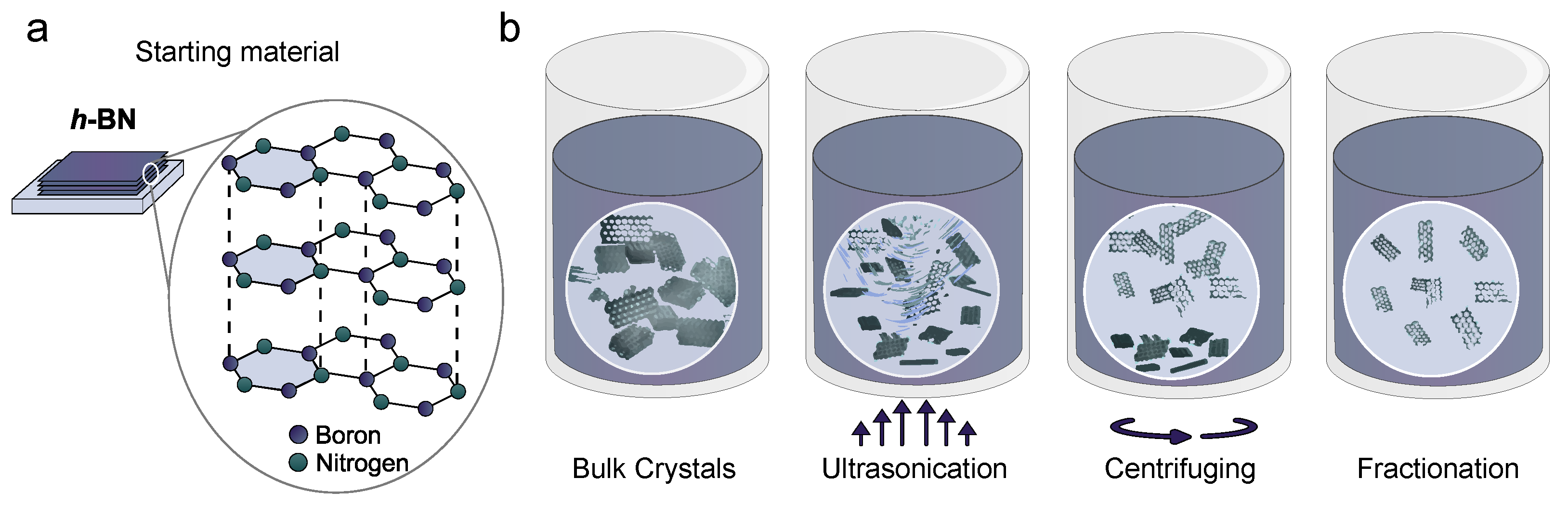
Abstract
1. Introduction
2. Materials and Methods
2.1. Sample Preparation
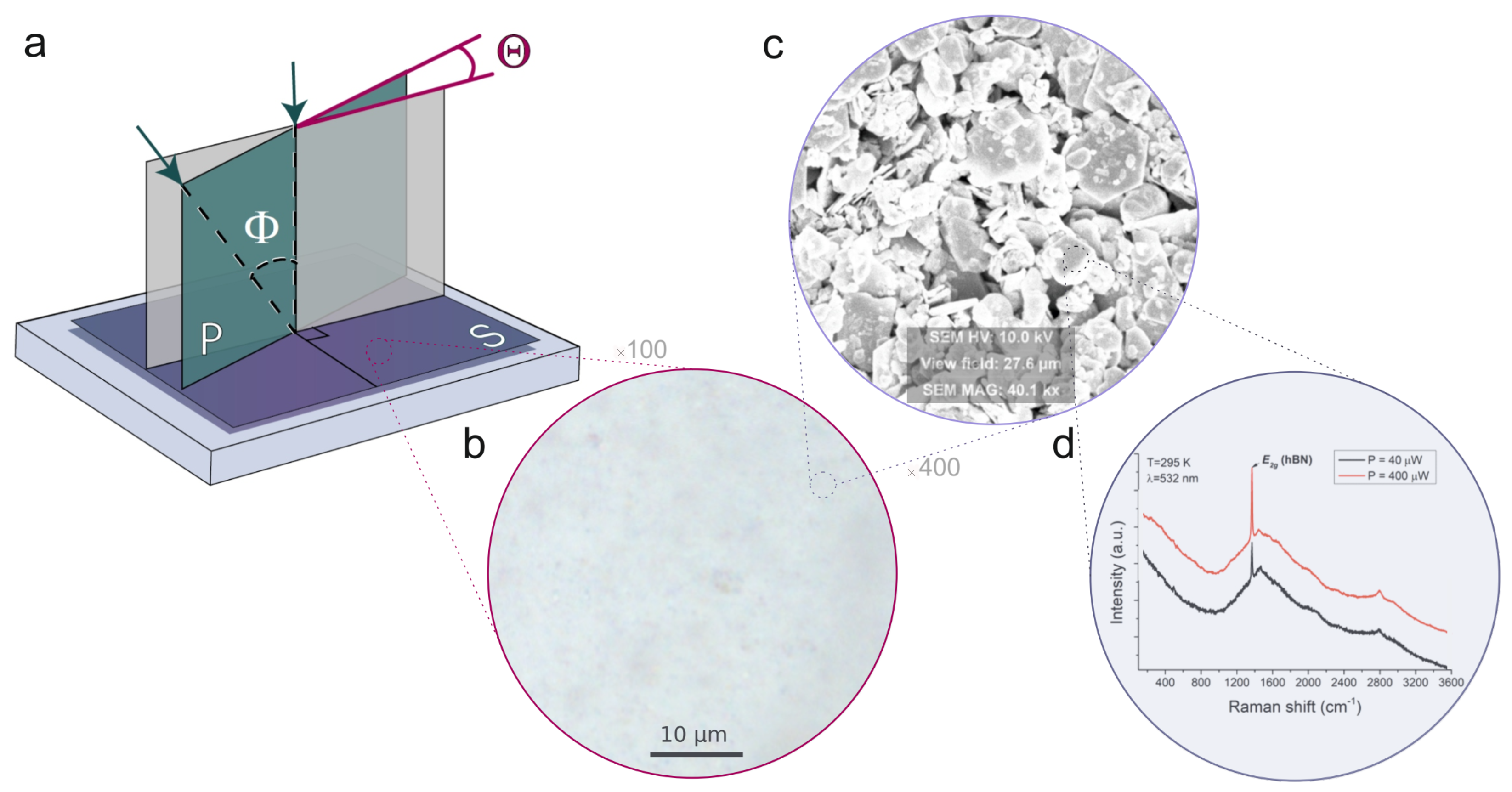
2.2. Optical Measurements
2.3. Optical Microscopy
2.4. Scanning Electron Microscopy (SEM)
2.5. Raman Spectroscopy
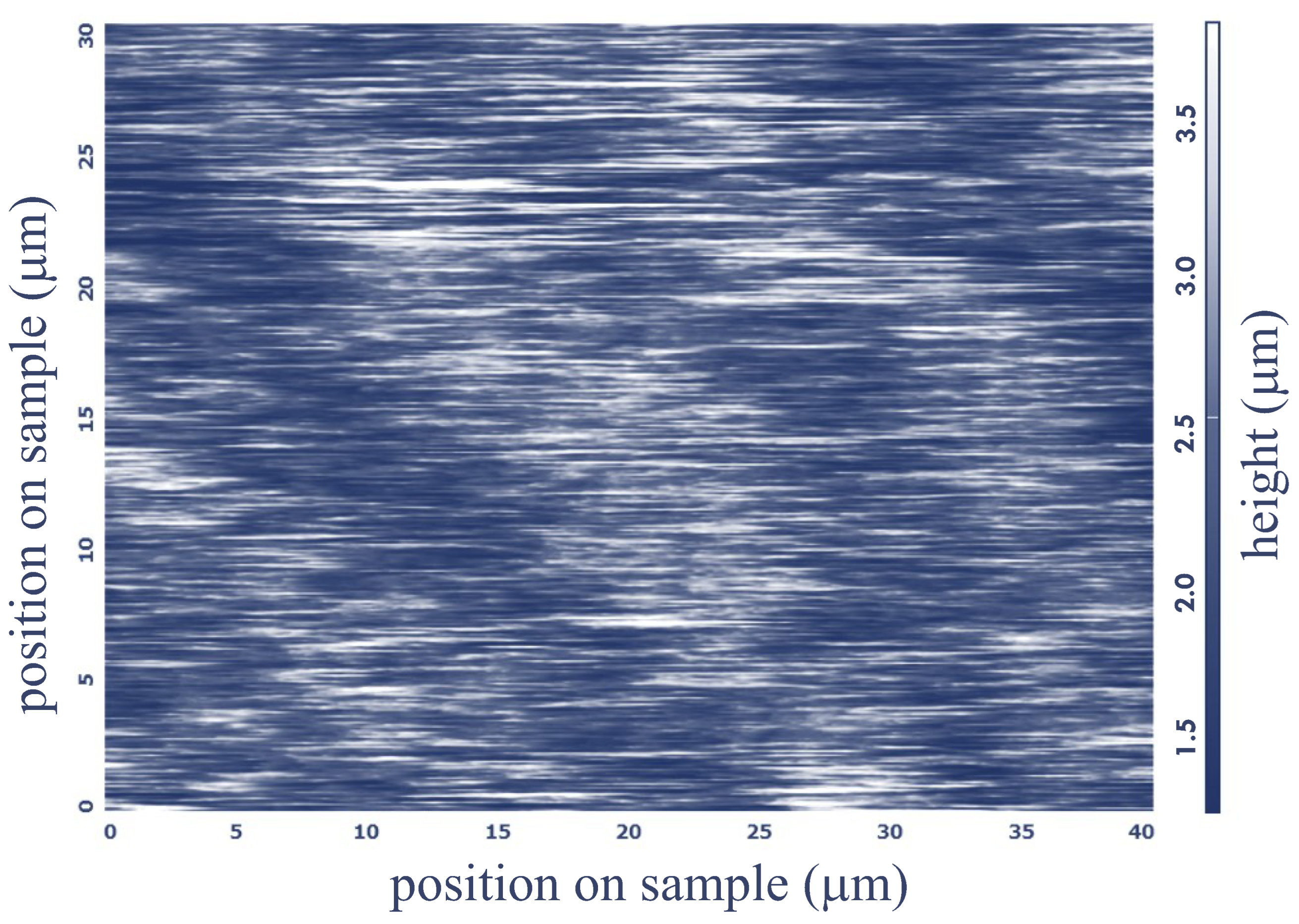
2.6. Atomic Force Microscopy (AFM)
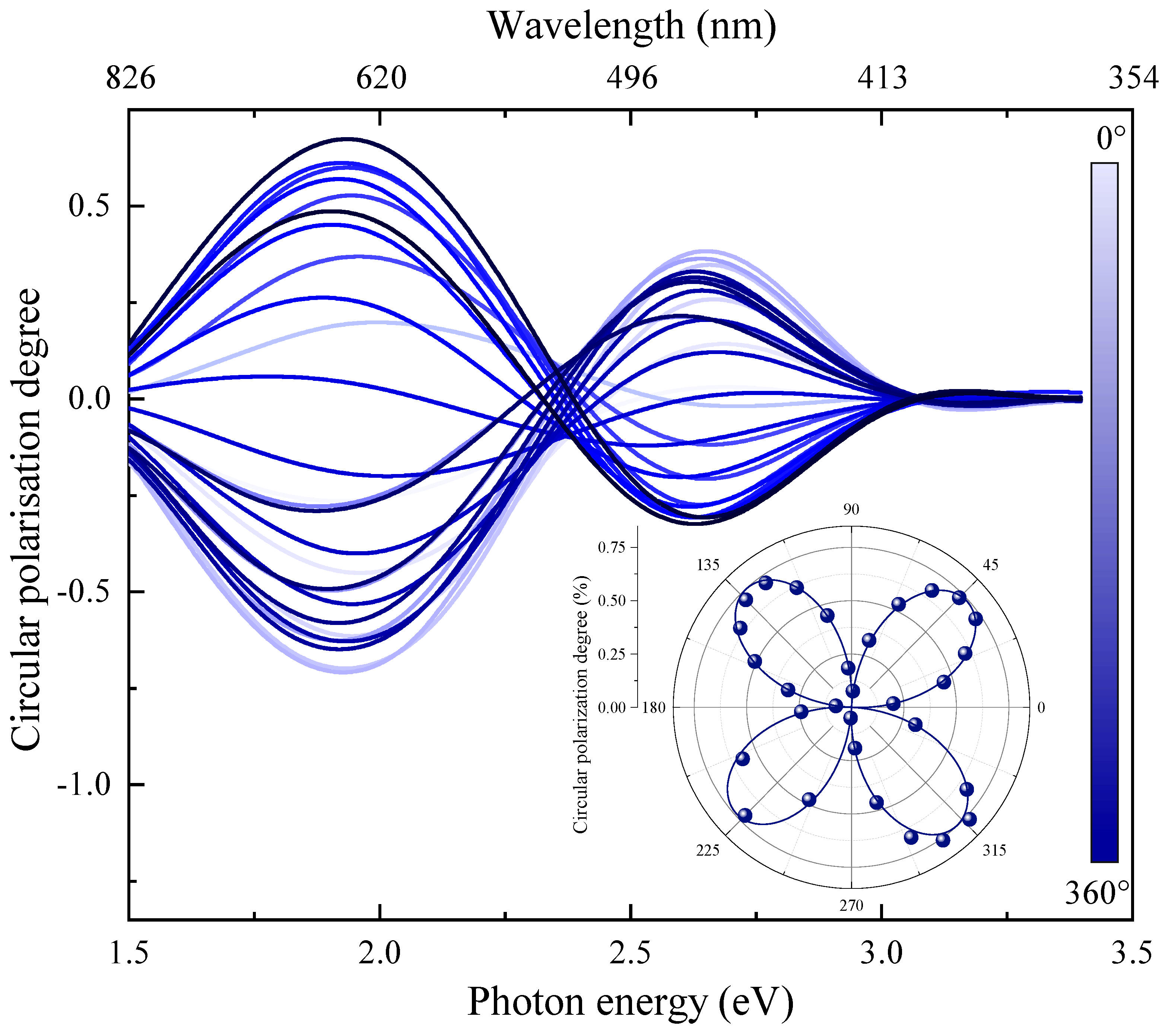
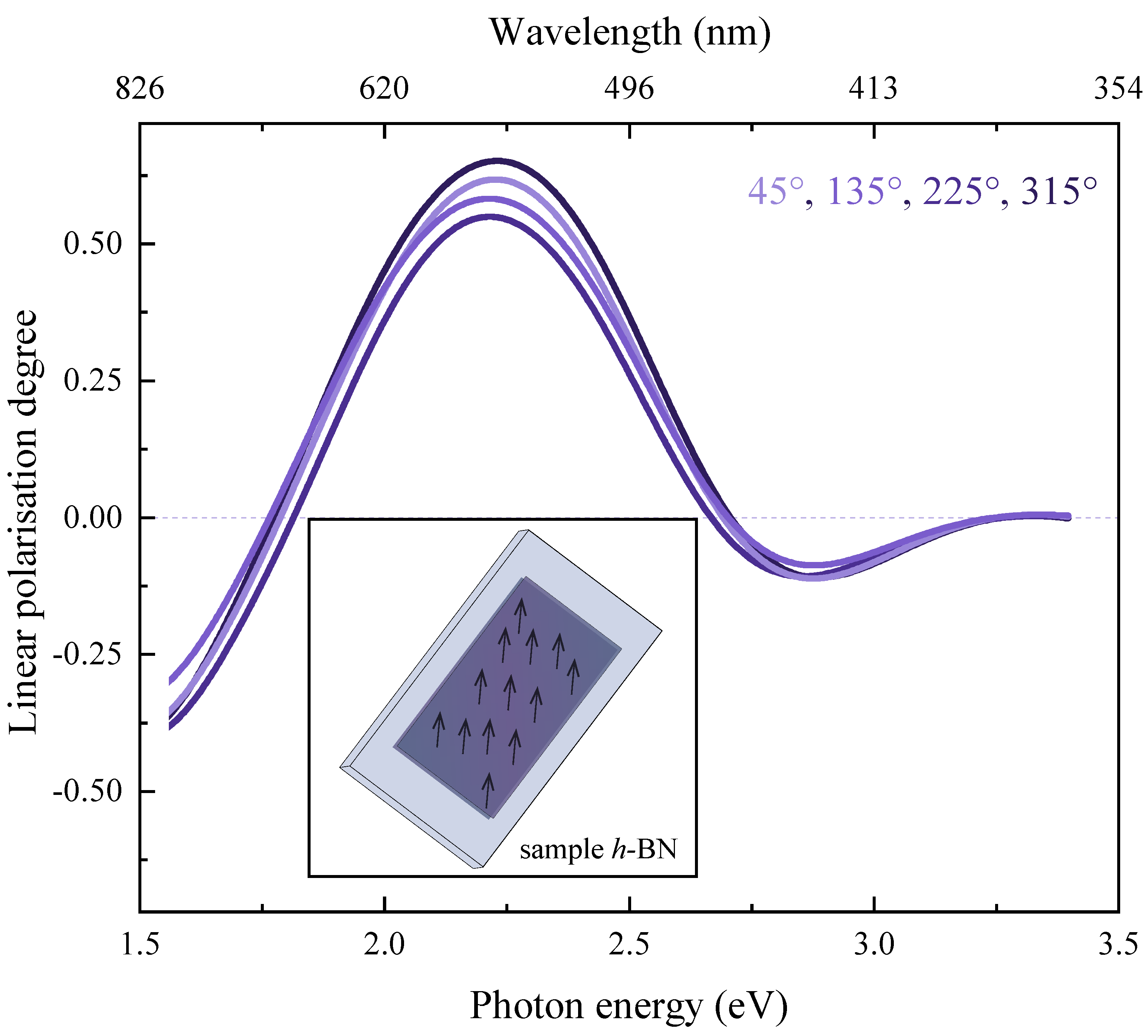
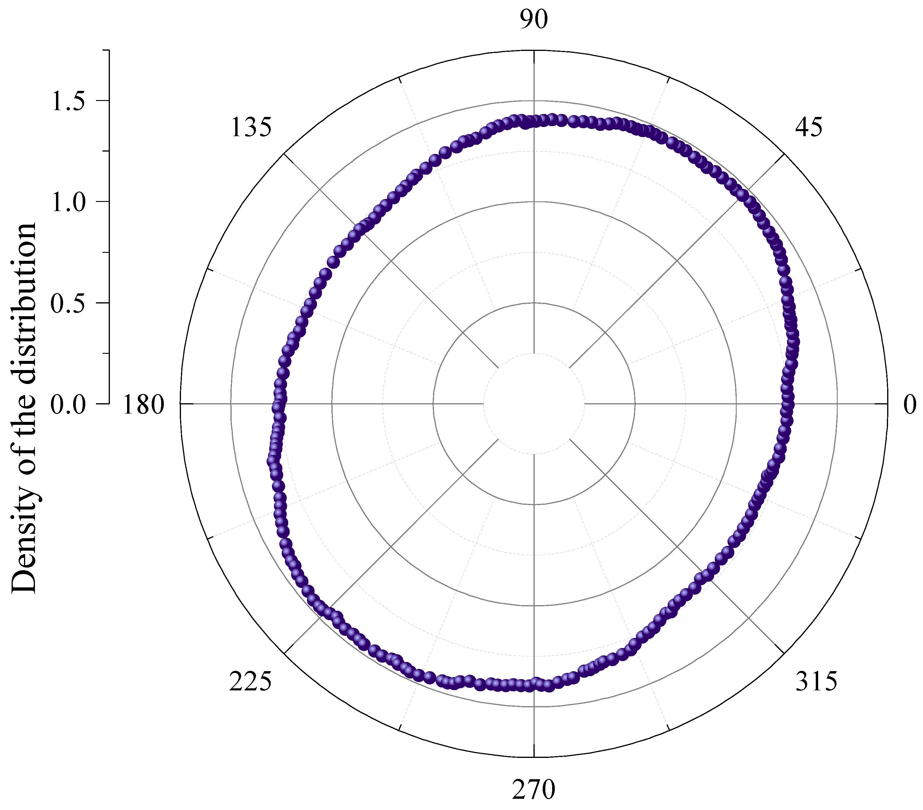
3. Results
4. Discussion
5. Conclusions
Author Contributions
Funding
Institutional Review Board Statement
Informed Consent Statement
Data Availability Statement
Conflicts of Interest
Abbreviations
| 2D | two-dimensional |
| h-BN | hexagonal boron nitride |
| PET | polyethylene terephthalate |
| PTFE | polytetrafluoroethylene |
| SEM | scanning electron microscopy |
| AFM | atomic force microscopy |
References
- Xu, J.; Peng, T.; Qin, X.; Zhang, Q.; Liu, T.; Dai, W.; Chen, B.; Yu, H.; Shi, S. Recent advances in 2D MXenes: Preparation, intercalation and applications in flexible devices. J. Mater. Chem. A 2021, 9, 14147–14171. [Google Scholar] [CrossRef]
- Pang, J.; Mendes, R.G.; Bachmatiuk, A.; Zhao, L.; Ta, H.Q.; Gemming, T.; Liu, H.; Liu, Z.; Rummeli, M.H. Applications of 2D MXenes in energy conversion and storage systems. Chem. Soc. Rev. 2019, 48, 72–133. [Google Scholar] [CrossRef]
- Manzeli, S.; Ovchinnikov, D.; Pasquier, D.; Yazyev, O.V.; Kis, A. 2D transition metal dichalcogenides. Nat. Rev. Mater. 2017, 2, 17033. [Google Scholar] [CrossRef]
- Rasul, M.G.; Kiziltas, A.; Arfaei, B.; Shahbazian-Yassar, R. 2D boron nitride nanosheets for polymer composite materials. npj 2D Mater. Appl. 2021, 5, 56. [Google Scholar] [CrossRef]
- Zhang, K.; Feng, Y.; Wang, F.; Yang, Z.; Wang, J. Two dimensional hexagonal boron nitride (2D-hBN): Synthesis, properties and applications. J. Mater. Chem. C 2017, 5, 11992–12022. [Google Scholar] [CrossRef]
- Khan, K.; Tareen, A.K.; Aslam, M.; Wang, R.; Zhang, Y.; Mahmood, A.; Ouyang, Z.; Zhang, H.; Guo, Z. Recent developments in emerging two-dimensional materials and their applications. J. Mater. Chem. C 2020, 8, 387–440. [Google Scholar] [CrossRef]
- Catania, F.; Marras, E.; Giorcelli, M.; Jagdale, P.; Lavagna, L.; Tagliaferro, A.; Bartoli, M. A Review on Recent Advancements of Graphene and Graphene-Related Materials in Biological Applications. Appl. Sci. 2021, 11, 614. [Google Scholar] [CrossRef]
- Tielrooij, K.J. Ultrafast light-based logic with graphene. Nat. Mater. 2022, 1–2. [Google Scholar] [CrossRef] [PubMed]
- Geim, A.; Grigorieva, I. Van der Waals heterostructures. Nature 2013, 499, 419–425. [Google Scholar] [CrossRef] [PubMed]
- Liu, L.; Zhai, T. Wafer-scale vertical van der Waals heterostructures. InfoMat 2021, 3, 3–21. [Google Scholar] [CrossRef]
- Fan, S.; Vu, Q.A.; Tran, M.D.; Adhikari, S.; Lee, Y.H. Transfer assembly for two-dimensional van der Waals heterostructures. 2D Mater. 2020, 7, 022005. [Google Scholar] [CrossRef]
- Guo, B.; Xiao, Q.l.; Wang, S.h.; Zhang, H. 2D Layered Materials: Synthesis, Nonlinear Optical Properties, and Device Applications. Laser Photonics Rev. 2019, 13, 1800327. [Google Scholar] [CrossRef]
- Xiao, X.; Wang, H.; Urbankowski, P.; Gogotsi, Y. Topochemical synthesis of 2D materials. Chem. Soc. Rev. 2018, 47, 8744–8765. [Google Scholar] [CrossRef] [PubMed]
- Mannix, A.J.; Kiraly, B.; Hersam, M.C.; Guisinger, N.P. Synthesis and chemistry of elemental 2D materials. Nat. Rev. Chem. 2017, 1, 0014. [Google Scholar] [CrossRef]
- Karfa, P.; Chandra Majhi, K.; Madhuri, R. Chapter 2—Synthesis of two-dimensional nanomaterials. In Two-Dimensional Nanostructures for Biomedical Technology; Khan, R., Barua, S., Eds.; Elsevier: Amsterdam, The Netherlands, 2020; pp. 35–71. [Google Scholar] [CrossRef]
- Shen, P.C.; Lin, Y.; Wang, H.; Park, J.H.; Leong, W.S.; Lu, A.Y.; Palacios, T.; Kong, J. CVD Technology for 2-D Materials. IEEE Trans. Electron Devices 2018, 65, 4040–4052. [Google Scholar] [CrossRef]
- Seredyński, B.; Ogorzałek, Z.; Zajkowska, W.; Bożek, R.; Tokarczyk, M.; Suffczyński, J.; Kret, S.; Sadowski, J.; Gryglas-Borysiewicz, M.; Pacuski, W. Molecular Beam Epitaxy of a 2D Material Nearly Lattice Matched to a 3D Substrate: NiTe2 on GaAs. Cryst. Growth Des. 2021, 21, 5773–5779. [Google Scholar] [CrossRef]
- Ba, H.; Truong-Phuoc, L.; Pham-Huu, C.; Luo, W.; Baaziz, W.; Romero, T.; Janowska, I. Colloid Approach to the Sustainable Top-Down Synthesis of Layered Materials. ACS Omega 2017, 2, 8610–8617. [Google Scholar] [CrossRef]
- Wang, X.Y.; Narita, A.; Müllen, K. Precision synthesis versus bulk-scale fabrication of graphenes. Nat. Rev. Chem. 2018, 2, 0100. [Google Scholar] [CrossRef]
- Novoselov, K.S. Electric Field Effect in Atomically Thin Carbon Films. Science 2004, 306, 666–669. [Google Scholar] [CrossRef]
- Niu, L.; Coleman, J.N.; Zhang, H.; Shin, H.; Chhowalla, M.; Zheng, Z. Production of Two-Dimensional Nanomaterials via Liquid-Based Direct Exfoliation. Small 2016, 12, 272–293. [Google Scholar] [CrossRef]
- Jalili, R.; Aminorroaya-Yamini, S.; Benedetti, T.M.; Aboutalebi, S.H.; Chao, Y.; Wallace, G.G.; Officer, D.L. Processable 2D materials beyond graphene: MoS2 liquid crystals and fibres. Nanoscale 2016, 8, 16862–16867. [Google Scholar] [CrossRef]
- Hogan, B.T.; Kovalska, E.; Zhukova, M.O.; Yildirim, M.; Baranov, A.; Craciun, M.F.; Baldycheva, A. 2D WS2 liquid crystals: Tunable functionality enabling diverse applications. Nanoscale 2019, 11, 16886–16895. [Google Scholar] [CrossRef] [PubMed]
- Hogan, B.T.; Kovalska, E.; Craciun, M.F.; Baldycheva, A. 2D material liquid crystals for optoelectronics and photonics. J. Mater. Chem. C 2017, 5, 11185–11195. [Google Scholar] [CrossRef]
- Shaban, P.; Oparin, E.; Zhukova, M.; Hogan, B.; Kovalska, E.; Baldycheva, A.; Tsypkin, A. Transmission properties of van der Waals materials for terahertz time-domain spectroscopy applications. AIP Conf. Proc. 2020, 2300, 020111. [Google Scholar] [CrossRef]
- Zhukova, M.; Hogan, B.; Oparin, E.; Shaban, P.; Grachev, Y.; Kovalska, E.; Walsh, K.; Craciun, M.; Baldycheva, A.; Tcypkin, A. Transmission Properties of FeCl3-Intercalated Graphene and WS2 Thin Films for Terahertz Time-Domain Spectroscopy Applications. Nanoscale Res. Lett. 2019, 14, 225. [Google Scholar] [CrossRef]
- Brant, J.; Brunetta, C.; Aitken, J. 5.09 - Chalcogenides and Nonoxides. In Comprehensive Inorganic Chemistry II (Second Edition), 2nd ed.; Reedijk, J., Poeppelmeier, K., Eds.; Elsevier: Amsterdam, The Netherlands, 2013; pp. 213–283. [Google Scholar] [CrossRef]
- Eichler, J.; Lesniak, C. Boron nitride (BN) and BN composites for high-temperature applications. J. Eur. Ceram. Soc. 2008, 28, 1105–1109, Engineering Ceramics '07: From Engineering To Functionality. [Google Scholar] [CrossRef]
- Kostoglou, N.; Polychronopoulou, K.; Rebholz, C. Thermal and chemical stability of hexagonal boron nitride (h-BN) nanoplatelets. Vacuum 2015, 112, 42–45. [Google Scholar] [CrossRef]
- Joy, J.; George, E.; Haritha, P.; Thomas, S.; Anas, S. An overview of boron nitride based polymer nanocomposites. J. Polym. Sci. 2020, 58, 3115–3141. [Google Scholar] [CrossRef]
- Song, W.L.; Wang, P.; Cao, L.; Anderson, A.; Meziani, M.J.; Farr, A.J.; Sun, Y.P. Polymer/Boron Nitride Nanocomposite Materials for Superior Thermal Transport Performance. Angew. Chem. Int. Ed. 2012, 51, 6498–6501. [Google Scholar] [CrossRef]
- Moon, P.; Koshino, M. Electronic properties of graphene/hexagonal-boron-nitride moiré superlattice. Phys. Rev. B 2014, 90, 155406. [Google Scholar] [CrossRef]
- Ronning, C.; Banks, A.; McCarson, B.; Schlesser, R.; Sitar, Z.; Davis, R.; Ward, B.; Nemanich, R. Structural and electronic properties of boron nitride thin films containing silicon. J. Appl. Phys. 1998, 84, 5046–5051. [Google Scholar] [CrossRef]
- Kotova, L.V.; Altynbaev, L.A.; Zhukova, M.O.; Hogan, B.T.; Baldycheva, A.; Kurbatov, D.M.; Kochereshko, V.P. Anisotropy of Optical Properties of Hexagonal Boron Nitride Films. Phys. Solid State 2021, 63, 1437–1441. [Google Scholar] [CrossRef]
- Kotova, L.V.; Altynbaev, L.A.; Zhukova, M.O.; Hogan, B.T.; Baldycheva, A.; Kaliteevski, M.A.; Kochereshko, V.P. Anisotropic Optical Properties of Hexagonal Boron Nitride Films. Bull. Russ. Acad. Sci. Phys. 2022, 86, 813–816. [Google Scholar] [CrossRef]
- Backes, C.; Higgins, T.M.; Kelly, A.; Boland, C.; Harvey, A.; Hanlon, D.; Coleman, J.N. Guidelines for Exfoliation, Characterization and Processing of Layered Materials Produced by Liquid Exfoliation. Chem. Mater. 2017, 29, 243–255. [Google Scholar] [CrossRef]
- Coleman, J.N.; Lotya, M.; O’Neill, A.; Bergin, S.D.; King, P.J.; Khan, U.; Young, K.; Gaucher, A.; De, S.; Smith, R.J.; et al. Two-Dimensional Nanosheets Produced by Liquid Exfoliation of Layered Materials. Science 2011, 331, 568–571. [Google Scholar] [CrossRef]
- Habib, T.; Sundaravadivelu Devarajan, D.; Khabaz, F.; Parviz, D.; Achee, T.C.; Khare, R.; Green, M.J. Cosolvents as Liquid Surfactants for Boron Nitride Nanosheet (BNNS) Dispersions. Langmuir 2016, 32, 11591–11599. [Google Scholar] [CrossRef]
- Akbari, A.; Sheath, P.; Martin, S.; Shinde, D.; Shaibani, M.; Banerjee, P.; Tkacz, R.; Bhattacharyya, D.; Majumder, M. Large-area graphene-based nanofiltration membranes by shear alignment of discotic nematic liquid crystals of graphene oxide. Nat. Commun. 2016, 7, 10891. [Google Scholar] [CrossRef]
- Fu, K.; Wang, Y.; Yan, C.; Yao, Y.; Chen, Y.; Dai, J.; Lacey, S.; Wang, Y.; Wan, J.; Li, T.; et al. Graphene Oxide-Based Electrode Inks for 3D-Printed Lithium-Ion Batteries. Adv. Mater. 2016, 28, 2587–2594. [Google Scholar] [CrossRef]
- Kotova, L.; Platonov, A.; Poshakinsky, A.; Shubina, T. Polarization Conversion in MoS2 Flakes. Semiconductors 2020, 54, 1509–1513. [Google Scholar] [CrossRef]
- Kotova, L.V.; Rakhlin, M.V.; Galimov, A.I.; Eliseyev, I.A.; Borodin, B.R.; Platonov, A.V.; Kirilenko, D.A.; Poshakinskiy, A.V.; Shubina, T.V. MoS2 flake as a van der Waals homostructure: Luminescence properties and optical anisotropy. Nanoscale 2021, 13, 17566–17575. [Google Scholar] [CrossRef]
- Jacucci, G.; Bertolotti, J.; Vignolini, S. Role of Anisotropy and Refractive Index in Scattering and Whiteness Optimization. Adv. Opt. Mater. 2019, 7, 1900980. [Google Scholar] [CrossRef]
- Segura, A.; Artús, L.; Cuscó, R.; Taniguchi, T.; Cassabois, G.; Gil, B. Natural optical anisotropy of h-BN: Highest giant birefringence in a bulk crystal through the mid-infrared to ultraviolet range. Phys. Rev. Mater. 2018, 2, 024001. [Google Scholar] [CrossRef]
- Thouless, D. Electrons in disordered systems and the theory of localization. Phys. Rep. 1974, 13, 93–142. [Google Scholar] [CrossRef]
- Landauer, R. Electrical conductivity in inhomogeneous media. Aip Conf. Proc. 1978, 40, 2–45. [Google Scholar] [CrossRef]
- Choy, T.C. Effective Medium Theory: Principles and Applications; Clarendon Press: Oxford, UK, 2016. [Google Scholar]
- Bruggeman, D.A.G. Berechnung verschiedener physikalischer Konstanten von heterogenen Substanzen. I. Dielektrizitätskonstanten und Leitfähigkeiten der Mischkörper aus isotropen Substanzen. Ann. Der Phys. 1935, 416, 636–664. [Google Scholar] [CrossRef]


Publisher’s Note: MDPI stays neutral with regard to jurisdictional claims in published maps and institutional affiliations. |
© 2022 by the authors. Licensee MDPI, Basel, Switzerland. This article is an open access article distributed under the terms and conditions of the Creative Commons Attribution (CC BY) license (https://creativecommons.org/licenses/by/4.0/).
Share and Cite
Kotova, L.V.; Altynbaev, L.A.; Zhukova, M.O.; Borodin, B.R.; Kochereshko, V.P.; Baldycheva, A.; Hogan, B.T. Boron Nitride Thin Films with Anisotropic Optical Properties from Microscale Particle Density Distributions. Coatings 2022, 12, 1571. https://doi.org/10.3390/coatings12101571
Kotova LV, Altynbaev LA, Zhukova MO, Borodin BR, Kochereshko VP, Baldycheva A, Hogan BT. Boron Nitride Thin Films with Anisotropic Optical Properties from Microscale Particle Density Distributions. Coatings. 2022; 12(10):1571. https://doi.org/10.3390/coatings12101571
Chicago/Turabian StyleKotova, Lyubov V., Linar A. Altynbaev, Maria O. Zhukova, Bogdan R. Borodin, Vladimir P. Kochereshko, Anna Baldycheva, and Benjamin T. Hogan. 2022. "Boron Nitride Thin Films with Anisotropic Optical Properties from Microscale Particle Density Distributions" Coatings 12, no. 10: 1571. https://doi.org/10.3390/coatings12101571
APA StyleKotova, L. V., Altynbaev, L. A., Zhukova, M. O., Borodin, B. R., Kochereshko, V. P., Baldycheva, A., & Hogan, B. T. (2022). Boron Nitride Thin Films with Anisotropic Optical Properties from Microscale Particle Density Distributions. Coatings, 12(10), 1571. https://doi.org/10.3390/coatings12101571