
Curved-Mechanical Characteristic Measurements of Transparent Conductive Film-Coated Polymer Substrates Using Common-Path Optical Interferometry


Abstract
:1. Introduction
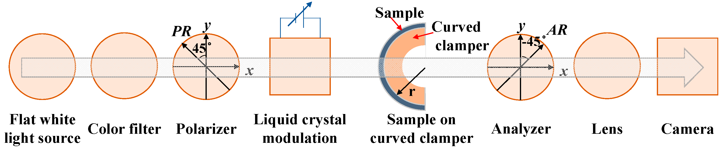
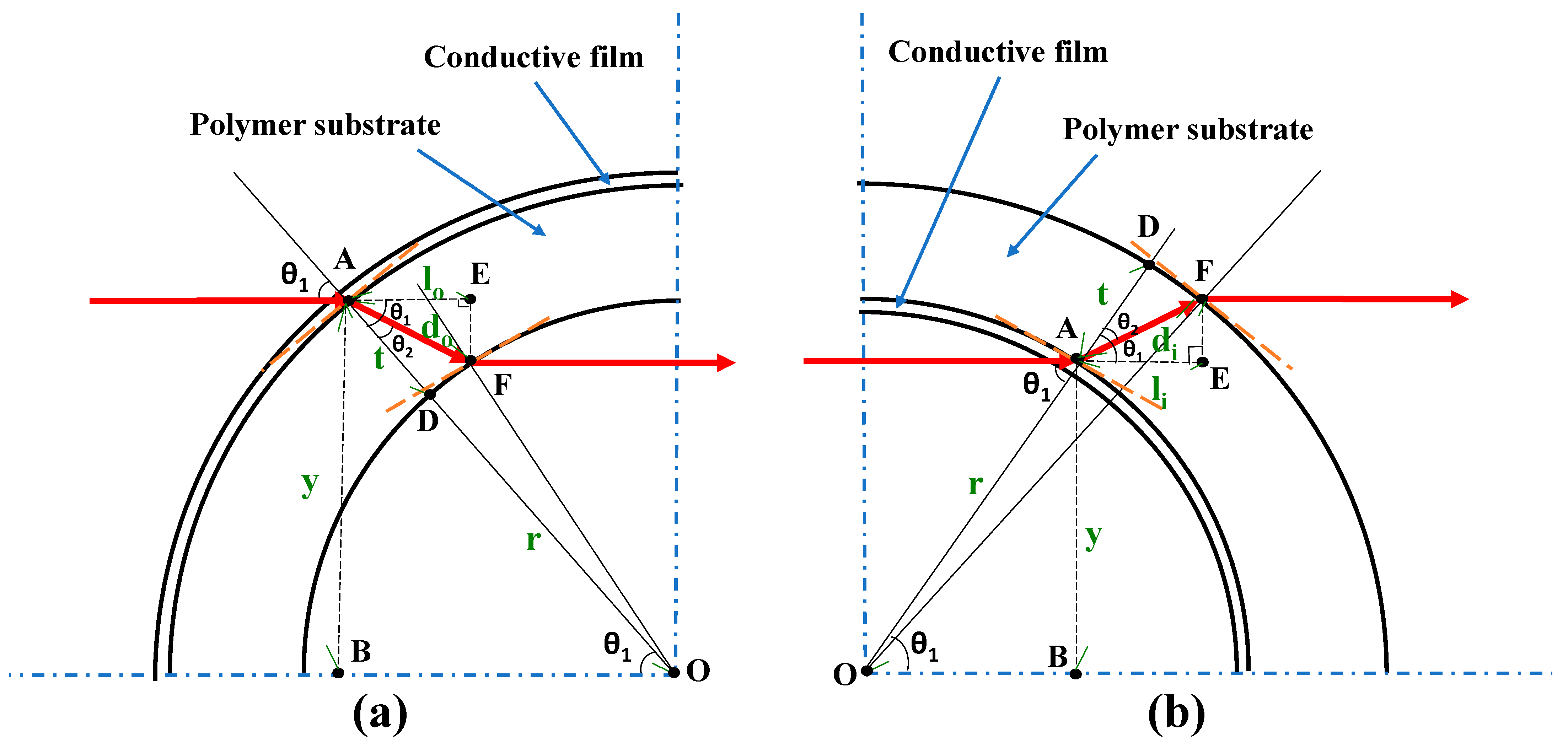
2. Methods
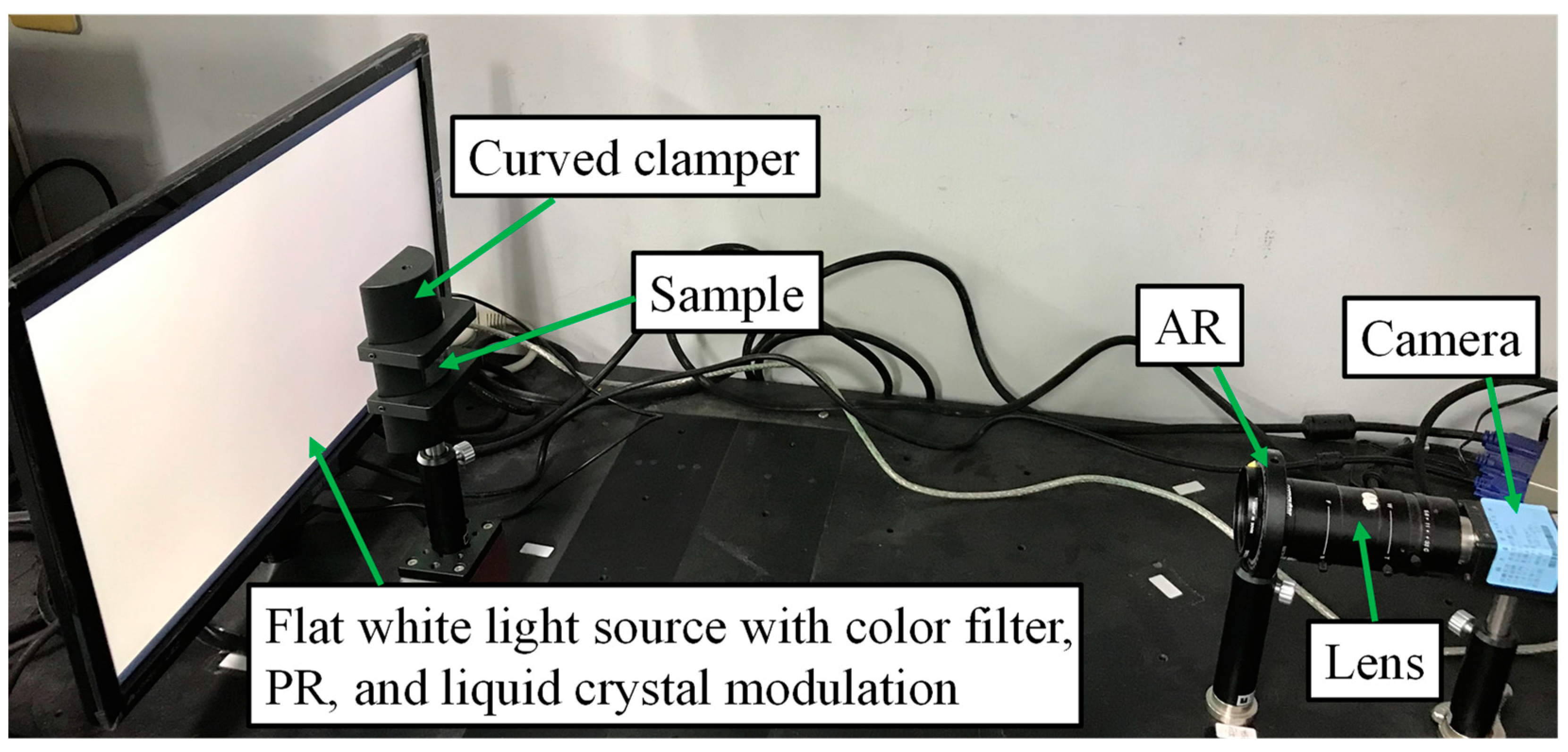
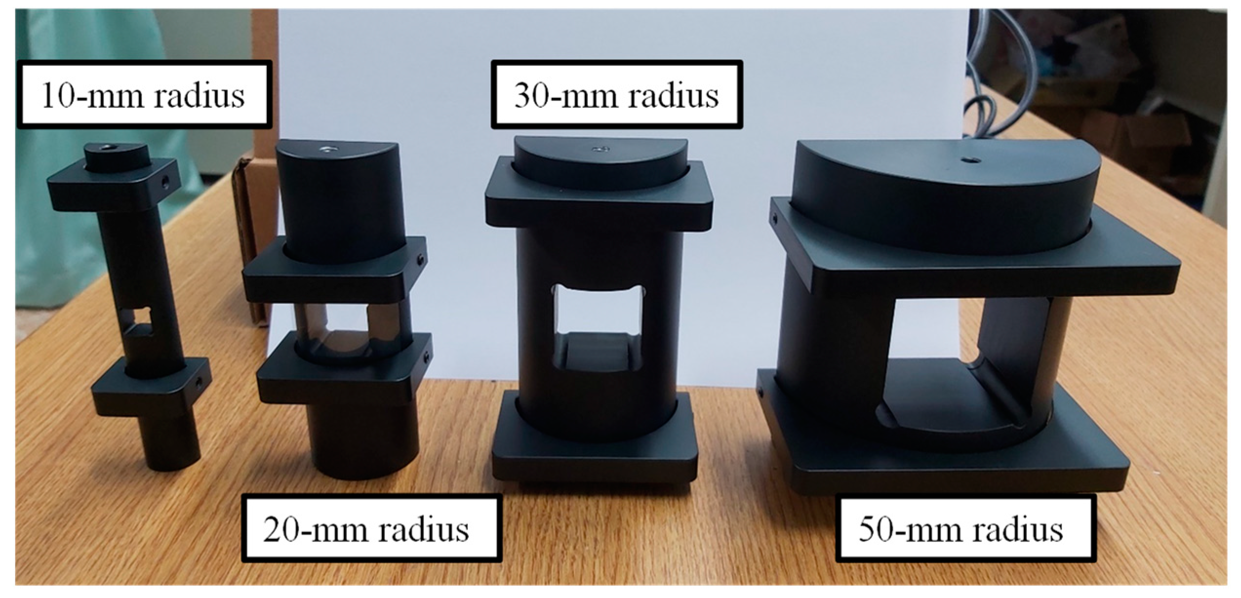
3. Experiment
4. Experimental Results and Discussion
5. Conclusions
Author Contributions
Funding
Conflicts of Interest
References
- Alqadami, A.S.M.; Jamlos, M.F.; Soh, P.J.; Kamarudin, M.R. Polymer (PDMS-Fe3O4) magneto-dielectric substrate for a MIMO antenna array. Appl. Phys. A 2016, 122, 9. [Google Scholar] [CrossRef]
- Economou, A.; Kokkinos, C.; Prodromidis, M. (Mamas) Flexible plastic, paper and textile lab-on-a chip platforms for electrochemical biosensing. Lab Chip 2018, 18, 1812–1830. [Google Scholar] [CrossRef] [PubMed]
- Chaudhary, K.; Singh, G.; Ramkumar, J.; Ramakrishna, S.A.; Srivastava, K.V.; Ramamurthy, P.C. Optically Transparent Protective Coating for ITO-Coated PET-Based Microwave Metamaterial Absorbers. IEEE Trans. Compon. Packag. Manuf. Technol. 2020, 10, 378–388. [Google Scholar] [CrossRef]
- Charmet, J.; Rodrigues, R.; Yildirim, E.; Challa, P.K.; Roberts, B.; Dallmann, R.; Whulanza, Y. Low-Cost Microfabrication Tool Box. Micromachines 2020, 11, 135. [Google Scholar] [CrossRef] [PubMed] [Green Version]
- Elakkiya, A.; Radha, S.; Sreeja, B.S.; Manikandan, E. Terahertz broadband metamaterial absorber enabled by SiO2SiO2, polyimide and PET dielectric substrates. Pramana 2020, 94, 1–6. [Google Scholar] [CrossRef]
- Li, H.; Dong, W.; Wu, X.; Xi, J.; Ji, Z. Resistive switching characteristics of ZnO/a-TiO2 bilayer film fabricated on PET/ITO transparent and flexible substrates. Mater. Res. Bull. 2016, 84, 449–454. [Google Scholar] [CrossRef]
- Kim, T.H.; Park, S.H.; Kim, D.H.; Nah, Y.C.; Kim, H.K. Roll-to-roll sputtered ITO/Ag/ITO multilayers for highly transparent and flexible electrochromic applications. Sol. Energy Mater. Sol. Cells 2017, 160, 203–210. [Google Scholar] [CrossRef]
- Shekargoftar, M.; Krumpolec, R.; Homola, T. Enhancement of electrical properties of flexible ITO/PET by atmospheric pressure roll-to-roll plasma. Mater. Sci. Semicond. Process. 2018, 75, 95–102. [Google Scholar] [CrossRef]
- Zhang, Y.; Pan, T.; Yang, Z. Flexible polyethylene terephthalate/polyaniline composite paper with bending durability and effective electromagnetic shielding performance. Chem. Eng. J. 2020, 389, 124433. [Google Scholar] [CrossRef]
- Song, W.-L.; Cao, M.-S.; Lu, M.-M.; Bi, S.; Wang, C.-Y.; Liu, J.; Yuan, J.; Fan, L.-Z. Flexible graphene/polymer composite films in sandwich structures for effective electromagnetic interference shielding. Carbon 2014, 66, 67–76. [Google Scholar] [CrossRef]
- Alam, A.; Meng, Q.; Shi, G.; Arabi, S.; Ma, J.; Zhao, N.; Kuan, H.C. Electrically conductive, mechanically robust, pH-sensitive graphene/polymer composite hydrogels. Compos. Sci. Technol. 2016, 127, 119–126. [Google Scholar] [CrossRef]
- Li, A.; Zhang, C.; Zhang, Y.F. Thermal conductivity of graphene-polymer composites: Mechanisms, properties, and applications. Polymers 2017, 9, 437. [Google Scholar]
- Kumari, S.; Panigrahi, A.; Singh, S.K.; Pradhan, S.K. Enhanced corrosion resistance and mechanical properties of nanostructured graphene-polymer composite coating on copper by electrophoretic deposition. J. Coat. Technol. Res. 2018, 15, 583–592. [Google Scholar] [CrossRef]
- Zhang, M.; Wang, X.; Yang, T.; Zhang, P.; Wei, X.; Zhang, L.; Li, H. Polyaniline/graphene hybrid fibers as electrodes for flexible supercapacitors. Synth. Met. 2020, 268, 116484. [Google Scholar] [CrossRef]
- Suzuki, T.; Itoh, T.; Vantasin, S.; Minami, S.; Kutsuma, Y.; Ashida, K.; Kaneko, T.; Morisawa, Y.; Miura, T.; Ozaki, Y. Tip-enhanced Raman spectroscopic measurement of stress change in the local domain of epitaxial graphene on the carbon face of 4H-SiC (000–1). Phys. Chem. Chem. Phys. 2014, 16, 20236–20240. [Google Scholar] [CrossRef] [PubMed]
- Mishra, A.; Singh, V.K.; Mohanty, T. Coexistence of interfacial stress and charge transfer in graphene oxide-based magnetic nanocomposites. J. Mater. Sci. 2017, 52, 7677–7687. [Google Scholar] [CrossRef]
- Wang, C.; Wang, J.; Barber, A.H. Stress concentrations in nanoscale defective graphene. AIP Adv. 2017, 7, 115001. [Google Scholar] [CrossRef]
- Young, R.J.; Liu, M.; Kinloch, I.A.; Li, S.; Zhao, X.; Vallés, C.; Papageorgiou, D.G. The mechanics of reinforcement of polymers by graphene nanoplatelets. Compos. Sci. Technol. 2018, 154, 110–116. [Google Scholar] [CrossRef]
- Morgan, J.J.; Craciun, M.F.; Eichhorn, S.J. Quantification of stress transfer in a model cellulose nanocrystal/graphene bilayer using Raman spectroscopy. Compos. Sci. Technol. 2019, 177, 34–40. [Google Scholar] [CrossRef]
- Romero-Vargas Castrillón, S.; Perreault, F.; De Faria, A.F.; Elimelech, M. Interaction of graphene oxide with bacterial cell membranes: Insights from force spectroscopy. Environ. Sci. Technol. Lett. 2015, 2, 112–117. [Google Scholar] [CrossRef]
- Gupta, S.; McDonald, B.; Carrizosa, S.B.; Price, C. Microstructure, residual stress, and intermolecular force distribution maps of graphene/polymer hybrid composites: Nanoscale morphology-promoted synergistic effects. Compos. Part B Eng. 2016, 92, 175–192. [Google Scholar] [CrossRef]
- Li, Z.; Young, R.J.; Papageorgiou, D.G.; Kinloch, I.A.; Zhao, X.; Yang, C.; Hao, S. Interfacial stress transfer in strain engineered wrinkled and folded graphene. 2D Mater. 2019, 6, 045026. [Google Scholar] [CrossRef]
- Wen, B.J.; Liu, T.S. Edge contrast failure analysis on vision angle of human eyes for curve displays. J. Disp. Technol. 2012, 8, 418–423. [Google Scholar] [CrossRef]
- Sinitski, E.H.; Thompson, A.A.; Godsell, P.; Honey, J.; Besemann, M. Postural stability and simulator sickness after walking on a treadmill in a virtual environment with a curved display. Displays 2018, 52, 1–7. [Google Scholar] [CrossRef]
- Kim, Y.G.; Han, K.Y. Spread characteristics of OCR lamination for flexible OLED display process with flat and curved substrates. Jpn. J. Appl. Phys. 2021, 60, 056504. [Google Scholar] [CrossRef]
- Sharpe, W.N. Springer Handbook of Experimental Solid Mechanics; Springer Science & Business Media: Berlin/Heidelberg, Germany, 2008. [Google Scholar]
- Hecht, E. Optics, 4th ed.; Reading; Addison-Wesley: Boston, MA, USA, 2002. [Google Scholar]
- Lee, Y.C.; Liu, T.S.; Wu, C.I.; Lin, W.Y. Investigation on residual stress and stress-optical coefficient for flexible electronics by photoelasticity. Measurement 2012, 45, 311–316. [Google Scholar] [CrossRef]
- Lin, Y.; Zhou, Z.; Wang, R. Optical heterodyne measurement of the phase retardation of a quarter-wave plate. Opt. Lett. 1988, 13, 553–555. [Google Scholar]
- Nakadate, S. High precision retardation measurement using phase detection of Young’s fringes. Appl. Opt. 1990, 29, 242–246. [Google Scholar] [CrossRef]
- Lo, Y.L.; Lai, C.H.; Lin, J.F.; Hsu, P.F. Simultaneous absolute measurements of principle angle and phase retardation with a new common-path heterodyne interferometer. Appl. Opt. 2004, 43, 2013–2022. [Google Scholar] [CrossRef]
- Chen, Y.L.; Su, D.C. Full-field measurement of the phase retardation for birefringent elements by using common path heterodyne interferometry. Opt. Las. Eng. 2009, 47, 484–487. [Google Scholar] [CrossRef]
- Yu, T.C.; Lo, Y.L. A Highly Phase-Sensitive Heterodyne Polariscope for the Full-Field Measurement of Twisted- Nematic Liquid Crystal. IEEE Photonics Technol. Lett. 2008, 20, 1778–1780. [Google Scholar] [CrossRef]
- Chu, Y.C.; Chang, W.Y.; Chen, K.H.; Chen, J.H.; Tsai, B.C.; Hsu, K.Y. Full-field refractive index measurement with simultaneous phase-shift interferometry. Opt. Int. J. Light Electron Opt. 2014, 125, 3307–3310. [Google Scholar] [CrossRef]
- Wen, B.J.; Huang, S.A. Residual stress image inspections based on bending testing for flexible transparent conducting substrates by single-direction common-path image interferometry. IEEE Sens. J. 2018, 19, 1701–1709. [Google Scholar] [CrossRef]
- Aben, H.; Guillemet, C. Photoelasticity of Glass; Springer Science & Business Media: Berlin/Heidelberg, Germany, 2012. [Google Scholar]
- Quiroga, J.A.; Gómez-Pedrero, J.A. Application of principal component analysis in phase-shifting photoelasticity. Opt. Express 2016, 24, 5984–5995. [Google Scholar] [CrossRef] [Green Version]
- Júnior, P.M.; Vieira, F.G.; Magalhães, C.A.; Ribeiro, J.S.; Rios, I.G. Numerical method to digital photoelasticity using plane polariscope. Opt. Express 2016, 24, 12617–12624. [Google Scholar] [CrossRef]
- Probst, A.C.; Begou, T.; Döhring, T.; Zeising, S.; Stollenwerk, M.; Stadtmüller, J.; Emmerich, F.; Lumeau, J. Coating stress analysis and compensation for iridium-based x-ray mirrors. Appl. Opt. 2018, 57, 8775–8779. [Google Scholar] [CrossRef]
- Jena, S.; Tokas, R.B.; Tripathi, S.; Rao, K.D.; Udupa, D.V.; Thakur, S.; Sahoo, N.K. Influence of oxygen partial pressure on microstructure, optical properties, residual stress and laser induced damage threshold of amorphous HfO2 thin films. J. Alloys Compd. 2019, 771, 373–381. [Google Scholar] [CrossRef]
- Pan, L.; Qi, R.; Feng, Y.; Chen, J.; Zhang, Z.; Li, W.; Wang, Z. Effect of nitrogen doping on surface morphology, microstructure, chemical composition and intrinsic stress of nickel thin films deposited by reactive sputtering. Surf. Coat. Technol. 2019, 364, 196–203. [Google Scholar] [CrossRef]
- Wen, B.J.; Huang, S.A.; Tseng, T.Y. Experimental analysis of interfacial shear stress and electrical resistance of indium tin oxide-coated polyethylene terephthalate films for a whole folding test. J. Plast. Film Sheeting 2020, 36, 130–150. [Google Scholar] [CrossRef]
- Medhat, M.; Hendawy, N.I.; Zaki, A.A. Fringes of equal tangential inclination by curvature-induced birefringence. Opt. Laser Technol. 2003, 35, 31–35. [Google Scholar] [CrossRef]
- Wen, B.J.; Hsu, J.S.; Liu, W.C. Two-dimension phase-retardation distribution inspections for flexible displays by using full-field liquid-crystal modulating common-path interferometry. Jpn. J. Appl. Phys. 2014, 53, 05HB03. [Google Scholar] [CrossRef]
- Ghiglia, D.C.; Pritt, M.D. Two-Dimensional Phase Unwrapping: Theory, Algorithms, and Software; Wiley: New York, NY, USA, 1998. [Google Scholar]
- Malacara, D. Optical Shop Testing; John Wiley & Sons Inc.: Hoboken, NJ, USA, 2007. [Google Scholar]
- IEEE. Standard for Terminology and Test Methods for Analog-to-Digital Converters; IEEE Std. 1241-2000; IEEE: Piscataway, NJ, USA, 2000; pp. 25–29. [Google Scholar]
- Neerinck, D.G.; Vink, T.J. Depth profiling of thin ITO films by grazing incidence X-ray diffraction. Thin Solid Films 1996, 278, 12–17. [Google Scholar] [CrossRef]
- Lagazzo, A.; Moliner, C.; Bosio, B.; Botter, R.; Arato, E. Evaluation of the mechanical and thermal properties decay of PHBV/sisal and PLA/sisal biocomposites at different recycle steps. Polymers 2019, 11, 1477. [Google Scholar] [CrossRef] [PubMed] [Green Version]
- Gere, J.M.; Timoshenko, S.P. Mechanics of Materials; PWS-KENT Publishing Company: Boston, MA, USA, 1997. [Google Scholar]
- Cao, Q.; Geng, X.; Wang, H.; Wang, P.; Liu, A.; Lan, Y.; Peng, Q. A review of current development of graphene mechanics. Crystals 2018, 8, 357. [Google Scholar] [CrossRef] [Green Version]


| 50 mm | 30 mm | 20 mm | 10 mm |
|---|---|---|---|
| −3.19 rad | −3.31 rad | −3.43 rad | −3.47 rad |
| Radius (mm) | Folding Condition | Before 11,000 Whole-Folding Cycles | After 11,000 Whole-Folding Cycles | ||||
|---|---|---|---|---|---|---|---|
| 80-nm ITO (rad) | 160-nm ITO (Rad) | 230-nm ITO (Rad) | 80-nm ITO (Rad) | 160-nm ITO (Rad) | 230-nm ITO (Rad) | ||
| 50 | Outer | −2.15 | −1.23 | −3.75 | −2.09 | −1.27 | −3.81 |
| Inner | −1.63 | −0.62 | −3.62 | −1.76 | −0.38 | −3.65 | |
| 30 | Outer | −2.00 | −0.47 | −3.78 | −1.88 | −0.68 | −3.77 |
| Inner | −1.32 | −0.35 | −3.79 | −1.59 | −0.62 | −3.78 | |
| 20 | Outer | −2.18 | −0.87 | −3.75 | −1.97 | −0.50 | −3.71 |
| Inner | −2.04 | −0.56 | −3.74 | −2.22 | −1.05 | −3.69 | |
| 10 | Outer | −1.38 | −0.37 | −3.79 | −2.46 | −3.15 | −3.89 |
| Inner | −2.28 | 0.26 | −3.78 | −2.97 | −4.08 | −4.04 | |
| Radius (mm) | Folding Condition | Before 11,000 Whole-Folding Cycles | After 11,000 Whole-Folding Cycles | ||
|---|---|---|---|---|---|
| Graphene/PET 1 (Rad) | Graphene/PET 2 (Rad) | Graphene/PET 1 (Rad) | Graphene/PET 2 (Rad) | ||
| 50 | Outer | −4.02 | −4.51 | −3.81 | −4.41 |
| Inner | −1.97 | −4.12 | −2.95 | −4.28 | |
| 30 | Outer | −3.58 | −4.48 | −3.75 | −4.34 |
| Inner | −2.28 | −4.37 | −3.41 | −4.30 | |
| 20 | Outer | −3.75 | −4.50 | −3.74 | −4.43 |
| Inner | −2.15 | −4.38 | −3.24 | −4.41 | |
| 10 | Outer | −3.84 | −2.37 | −3.96 | −3.91 |
| Inner | −2.76 | −2.25 | −3.60 | −3.90 | |
Publisher’s Note: MDPI stays neutral with regard to jurisdictional claims in published maps and institutional affiliations. |
© 2021 by the authors. Licensee MDPI, Basel, Switzerland. This article is an open access article distributed under the terms and conditions of the Creative Commons Attribution (CC BY) license (https://creativecommons.org/licenses/by/4.0/).
Share and Cite
Wen, B.-J.; Hsu, J.-J. Curved-Mechanical Characteristic Measurements of Transparent Conductive Film-Coated Polymer Substrates Using Common-Path Optical Interferometry. Coatings 2021, 11, 766. https://doi.org/10.3390/coatings11070766
Wen B-J, Hsu J-J. Curved-Mechanical Characteristic Measurements of Transparent Conductive Film-Coated Polymer Substrates Using Common-Path Optical Interferometry. Coatings. 2021; 11(7):766. https://doi.org/10.3390/coatings11070766
Chicago/Turabian StyleWen, Bor-Jiunn, and Jui-Jen Hsu. 2021. "Curved-Mechanical Characteristic Measurements of Transparent Conductive Film-Coated Polymer Substrates Using Common-Path Optical Interferometry" Coatings 11, no. 7: 766. https://doi.org/10.3390/coatings11070766
APA StyleWen, B.-J., & Hsu, J.-J. (2021). Curved-Mechanical Characteristic Measurements of Transparent Conductive Film-Coated Polymer Substrates Using Common-Path Optical Interferometry. Coatings, 11(7), 766. https://doi.org/10.3390/coatings11070766