1. Introduction
In the current era, organic electronics have been extensively used in pure research for the last twenty years [
1]. The main attraction in this research area is the modification ability of organic framework which can tune directly the desired properties in the organic materials. The organic based semiconductor and other type of organic electronics have been tremendously replacing the conventional semiconductor such as silicon or gallium arsenide. A thin film light emitting diode was reported by Tang et al. with a very low voltage, which open the door for using organic thin films in optoelectronic devices [
2]. Some of the organic thin films such as organic light emitting device (OLED) have reached the consumer market, which have been used as a highly efficient and long lived color displays [
3,
4]. The organic thin film transistors [
5] and organic solar cells are very efficient and low-cost [
6].
The basic understanding of molecular and electronic level of the organic material is the key for designing a high performance electronic and optical organic device. Slight modification in the organic framework can markedly switch the properties of the bulk materials [
7]. The coropceanu et al. used theoretical methods to explore the different properties of organic materials by building a structure properties relationship. His finding is useful in understanding the existed devices and prediction of the ideal material for the next generation electronic and optoelectronic devices [
8].
The organic materials and their associated devices have similar electronic properties while different methods have been used for fabricating the organic and inorganic devices [
9]. By using organic compounds in electronic and optoelectronic devices, have opened a new door in fabricating techniques which are very efficient and potentially low cost [
10]. While in some cases it offers fabricating a way whichis inaccessible by conventional methods using conventional semiconductors. For instance, lithographic methods that govern inorganic devices were far behind the techniques available for processing and patterning organic materials [
11].
The size of nano-objects such as nanoparticles, nanorods or nanowires is comparable with the size of the biomaterials like enzymes, receptors, antigens/antibodies or folded DNA [
12]. By combining the nanomaterials with the biomolecules [
13] may result in hybrid materials that combine the evolutionary optimized recognition and catalytic properties of biomaterials with the unique electronic, optical and catalytic functions of nanomaterials [
14]. Nowadays, researchers are intentionally directed to synthesize bioelectronics systems by using biomolecules nanoparticles hybrid system [
15] which may be applied in the designing of electronic nanocircuitry, biosensors and even nanodevices [
16].
The current research article focuses on the photonics properties of afzelechin conjugated silver nanoparticles which can be used as a replacement to the other inorganic materials such as silica used for coating silver nanoparticles for photonic applications. This research will definitely open a new door in this research area as this is the pioneering work in this field.
2. Materials and Methods
The silver nitrate, afzelechin, and sodium hydroxide were purchased from Merck. The afzelechin conjugated silver nanoparticles were synthesized by mixing 0.1 mM solution of silver nitrate with 0.1 mM solution of afzelechin under stirring. Twenty minutes later, 1 mL of sodium hydroxide having 50 mM concentration was added as a reducing agent, which reduces silver ions to form afzelechin conjugated silver nanoparticles. The mixture was stirred by mean of an electric stirrer for 2 h. While bare silver nanoparticles were synthesized without afzelechin by mixing 0.1 mM solution of silver nitrate with 1 mL of sodium borohydride having 40 mM concentration [
17].
The afzelechin conjugated silver nanoparticles and bare silver nanoparticles were characterized via UV-Visible spectroscopy and atomic force microscopy techniques. The Shimadzu UV-240, Hitachi U-3200 spectrometer was used for recording UV-Visible spectra. The afzelechin conjugated silver nanoparticles were analyzed by mean of the AFM, made by Agilent Technologies 5500, USA, in the tapping mode. The sample was dried on freshly cleaved mica surface at room temperature. The AFM images were obtained using high frequency silicon (Si) cantilever having length of 125 micrometer (125 µm), with a force constant of 42 Newton per meter (42 N/m) and 330 KHz resonance frequency. The band gap energies of the afzelechin conjugated silver nanoparticles and bare silver nanoparticles were calculated and compared via Tauc’s equation, All the data were analyzed and plotted using OriginLab 9.0 software Northampton, MA, USA.
3. Results and Discussion
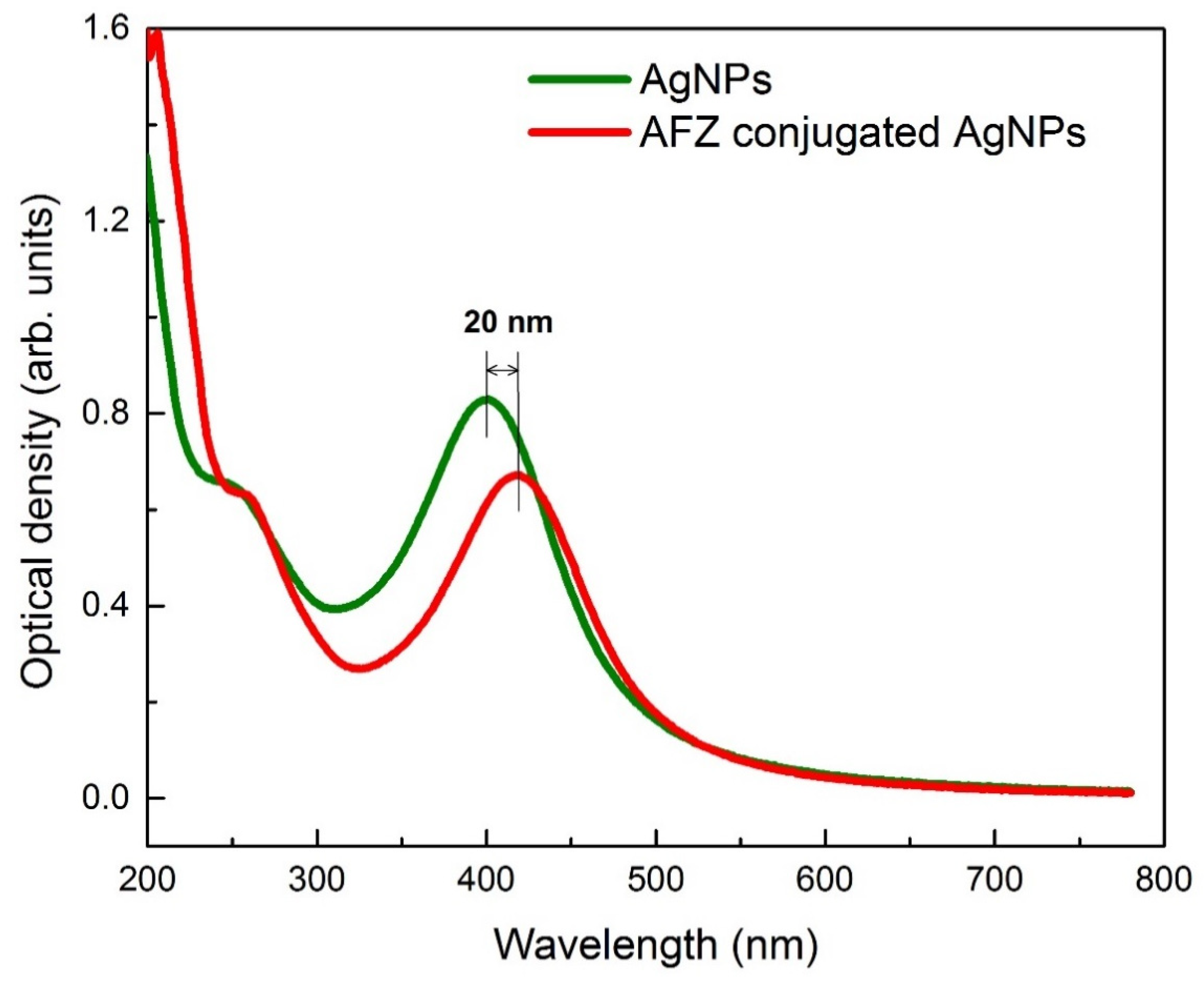
3.1. Synthesis and Characterization of Afzelechin Conjugated Silver Nanoparticles
A simple, one-pot reduction method was used for the synthesis of afzelechin conjugated silver nanoparticles and bare silver nanoparticles. The UV-Visible spectrum of the afzelechin conjugated silver nanoparticles showed the surface plasmon resonance (SPR) at 420 nm (
Figure 1) which is a characteristic of silver nanoparticles while UV-Visible spectrum of the bare silver nanoparticles showed SPR at 400 nm which is characteristic for bare silver nanoparticles as shown in the
Figure 1 [
18]. By comparing the UV-Visible spectra a difference of 20 nm was observed in the SPR wavelength (
Figure 1) which clearly indicates that afzelechin conjugation with AgNPs results in the red-shift SPR wavelength. The average size of bare silver and afzelechin conjugated silver nanoparticles is also calculated by fitting their UV-VIS absorption spectra. Fitting is based on the Mie and Mie Gans models, which account for the spherical and spheroidal morphologies of the nanoparticles, respectively. Details of the models and fitting parameters can be found in reference [
19].
For an accurate study of the morphology and distribution of nanoparticles, transmission electron microscopy is a powerful technique. However, in many cases, TEM comes with some limitations like modifications induced in NPs during the sample preparation, slow and laborious measurements. On the other hand, UV-VIS spectroscopy is an easy and fast measurement, which with the help of fitting models can provide information regarding the morphology and distribution of the NPs [
20].
Figure 1 reports the absorption spectra of bare and functionalized AgNPs in water solution. Typically, non-agglomerated AgNPs absorbed electromagnetic radiations at wavelengths less than 300 nm due to the interband transitions of d-band electrons and at above 400 nm due to the collective excitation of electrons associated with the NPs, called SPR [
21]. The location of SPR depended on the size of NPs and dielectric constant of the host matrix. In
Figure 1, SPR of AgNPs occurred at the edge of the visible region i.e., 400 nm, while for AgNPs functionalized with afzelechin took place at 420 nm. This 20 nm shift in the SPR may be attributed to an increase in the size of NPs due to conjugation with afzelechin. Variation in the absorbance at point close to plasmonic resonance indicated frequency dumping due to afzelechin conjugation. Electronic excitation generally takes place from the highest occupied molecular orbital (HOMO) to the least unoccupied molecular orbitals (LUMO). Conjugation of the afzelechin with AgNPs results in a reduction of energy difference between HOMO and LUMO due to the excitation of electrons at lower frequency. It is evident from the absorption profiles that the conjugation caused very small increase in the size of the NP, as size of the NP not only depends on the location of SPR but also on the width of absorption peak [
22,
23].
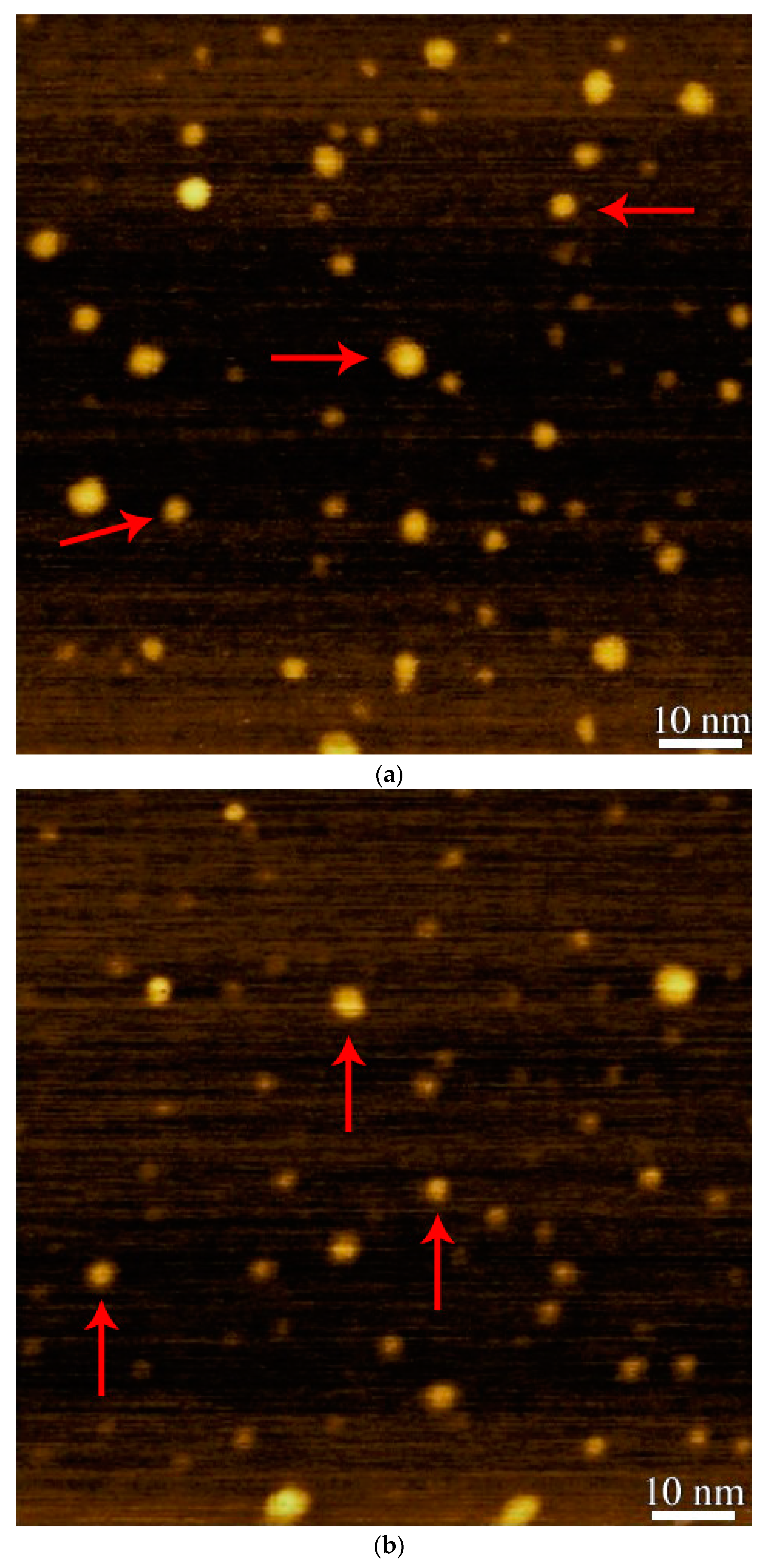
3.2. Atomic Force Microscopy
The AFM technique was used for the size determination of afzelechin conjugated silver nanoparticles and bare silver nanoparticles. The afzelechin conjugated silver nanoparticles and bare sliver nanoparticles were visualized under an AFM. The AFM results showed that afzelechin conjugated silver nanoparticles were spherical in shape and their sizes range from 3–10 nm with an average size of 6 nm, as shown in
Figure 2a. The bare silver nanoparticles were also spherical in shape and their sizes range from 3–10 nm with an average size of 8 nm, as shown in
Figure 2b. A difference of about 2 nm was observed in the sizes of afzelechin conjugated silver nanoparticles and bare silver nanoparticles which is responsible for the red shift in the SPR wavelength. The difference in size is due to conjugation of afzelechin molecules [
24].
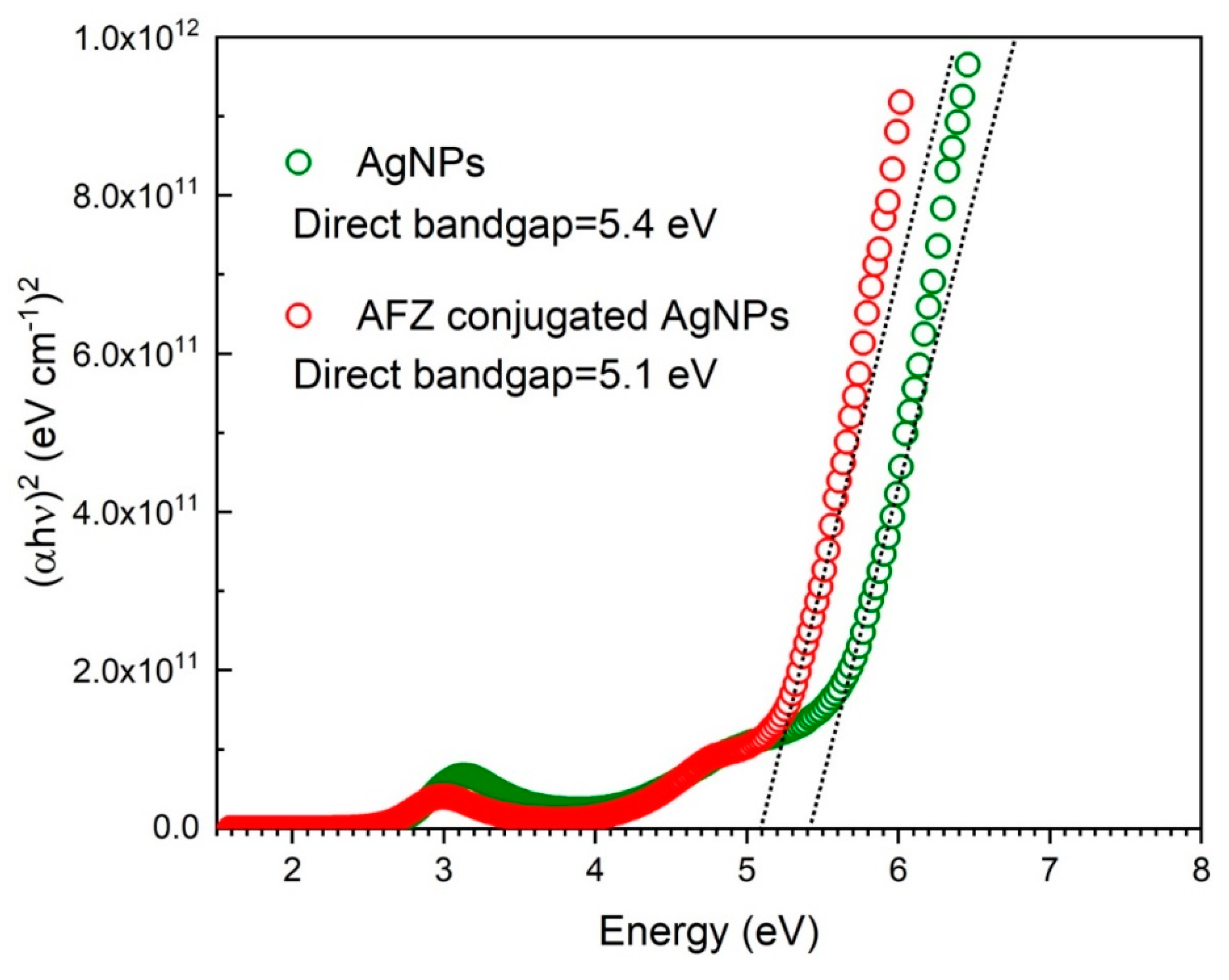
3.3. The Bandgap Energy
The bandgap energies of the bare and afzelechin conjugated AgNPs were calculated from their absorption spectra by utilizing the plot between
and energy. The nature and value of the optical bandgap
could be determined from the absorption spectrum corresponding to the excitation energy from the valence to the conduction band. The fundamental relation that relates the absorptions coefficient
and the photon energy
is
where
is a constant and
determines the nature of optical transition: such that, transition:
for a direct bandgap and
for an indirect gap material. The bandgap value could be determined from the slope of the plot between
and
.
Figure 3 shows the plot of
against the energy
of the incident photon for the bare AgNPs and afzelechin conjugated AgNPs. It was found that for the bare AgNPs, the optical transition was a direct allowed transition and the bandgap was 5.6 eV. While in the case of afzelechin conjugated AgNPs, the nature of the optical transition remained the same and its bandgap decreased to 5.2 eV. The decrease in the bandgap energy is attributed to the fact that afzelechin conjugation with AgNPs results in a reduction of HOMO-LUMO energy gap.
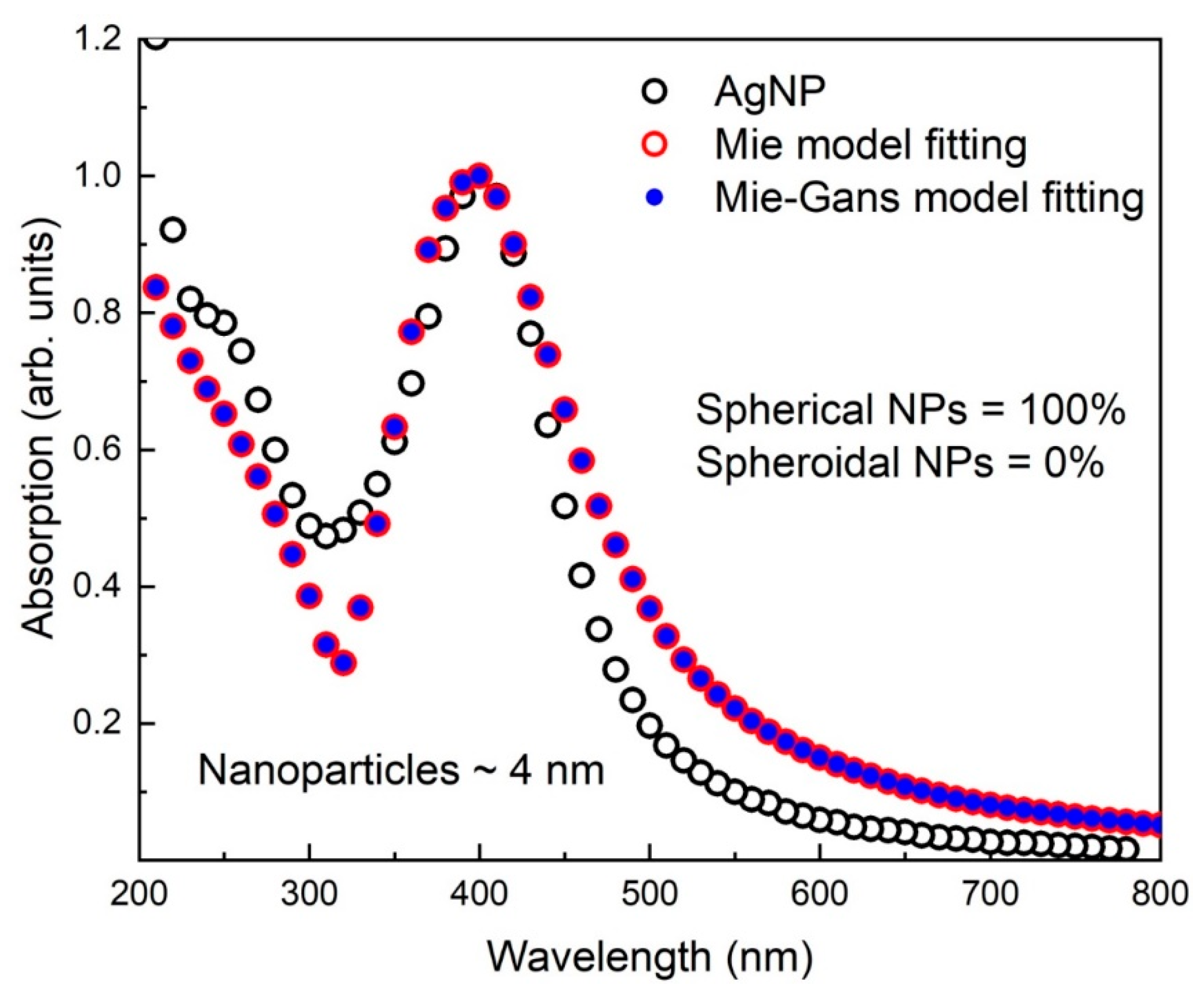
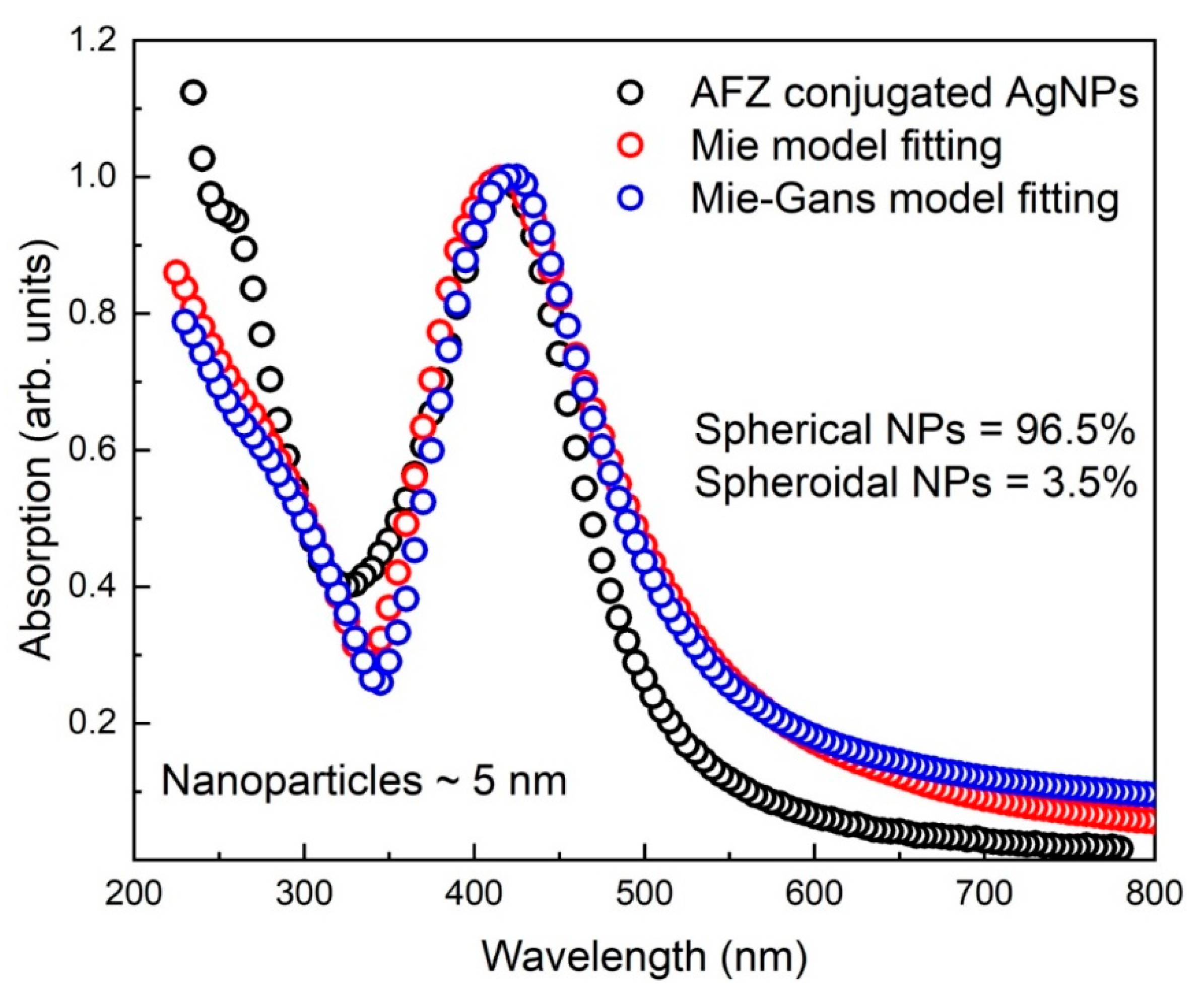
3.4. Mie and Mie-Gans Fitting Models
The absorption profiles can be effectively fitted with the Mie model for spherical nanoparticles. Mie model is based on the Maxwell equations which incorporate the discontinuity of the dielectric constants of host matrix and metal nanoparticle [
21]. The extension cross section
of a spherical nanoparticle of radius R is,
where
and
are the spherical Riccati Bessel functions, and m is the ratio of the refractive indices of the host matrix and the nanoparticle. The dielectric constant of a nanoparticle depends on the size of nanoparticle, which can be optimized by using R-dependent relaxation frequency
as,
where
is the bulk relaxation frequency,
is the Fermi velocity, and A is a practical value for optimizing size of the nanoparticle. As the size of a nanoparticle influenced the behavior of associated free electrons, which in turn played a vital role in plasmonic absorption, the dielectric constant of nanoparticles as function of frequency and radius of nanoparticle can be written as,
where,
is the dielectric function of bulk material [
21].
It is to be noted that Mie model alone cannot be used for fitting the absorption spectrum due to its validity for spherical particles only. In order to include deviation from spherical geometry, Gans model was used to account for the nonspherical particles. For spheroidal particles with aspect ratio
, the average absorption corss-section summed over all possible orientations is
where
is the volume of spheroid,
is the dielectric constant of the host material,
is the eccentricity and
is the wavelength of incident light. In Gans model, the Gaussian probability
(centered at
) for various nonspherical particles for
is [
25]
where
is the standard deviation. Hence, the combined Mie Gans model takes into account the radius of the nanoparticle, standard deviation from spherical geometry, and the ratio of spherical to spheroidal nanoparticles, to realize best fitting of the absorption spectra.
Figure 4 reports the absorption spectrum of the AgNPs normalized at SPR max in the range 200–780 nm. The fitting of the absorption spectrum was performed with the Mie and Mie Gans models, which deduced the size of the NPs as 4 nm. Fitting with the Mie and Mie Gans models overlapped due to the fact that all NPs were spherical in shape. A very good fit could be observed in the SPR range from 350–450 for experimental and calculated spectra, while in the range above 550 deviated slightly from the absorption profile due to the reason that Mie model was less sensitive for NPs having size around 4 nm [
26]. In the UV range from 200 to 300 nm where the effect of individual d-band electrons was dominant in water matrix, smooth fittings of the experimental spectrum were observed. Both the Mie and Mie-Gans fittings deduced the average extinction cross-section for single AgNP at the SPRmax as 3.75 × 10
−18 m
−2.
Figure 5 reports the absorption spectrum of the afzelechin conjugated AgNPs normalized at SPR max in the range 200–780 nm. Both the fitting models deduced an increase in the nanoparticle size, while the geometry of the spherical NPs changed slightly to spheroidal NPs due to conjugation with afzelechin. Majority of the NPs remained spherical and deviation from the spherical geometry occurred by only 3.5% on average due to conjugation. The fitting models deduced an increase in the size of conjugated NPs by 1 nm. A slight difference in the Mie and Mie Gans fittings clearly indicated the small change in the morphology of the NPs. It is also to be noted that the average extinction cross-section for a conjugated AgNP at the SPRmax increased by 13% due to conjugation. Moreover, very small broadening in the SPR indicated that new relaxation channels for plasmon excitations were being introduced by the afzelechin conjugation.
4. Conclusions
The afzelechin conjugated silver nanoparticles and bare silver nanoparticles were successfully synthesized and characterized via UV-Visible spectroscopy. A red-shift in the SPR of the silver nanoparticles was observed after conjugation with the afzelechin, which indicated an increase in the nanoparticle size. The Mie and Mie Gans fitting models were used for the determination of morphologies of these synthesized nanoparticles. As a result the afzelechin conjugated silver nanoparticles with an average size of 5 nm in which 96.5% were spherical and 3.5% were spheroidal in nature; while, the bare silver nanoparticles with an average size of 4 nm were found to be 100% spherical. While in the AFM images, the morphologies of afzelechin conjugated silver nanoparticles and bare silver nanoparticles were found to be spherical with sizes of 8 nm and 6 nm, respectively. The band gap energy of afzelechin conjugated silver nanoparticles and bare sliver nanoparticles were calculated via Tauc’s equation and were found to be 5.1 eV and 5.4 eV, respectively. A difference of around 0.3 eV was observed in the band gap energies of afzelechin conjugated AgNPs and bare AgNPs due to afzelechin conjugation. This result showed that conjugation of afzelechin with silver nanoparticles result a characteristics red-shift in the surface plasmon resonance wavelength, the size of silver nanoparticles were also increased, and the band gap energies were significantly reduced.
Author Contributions
Conceptualization, S.A., P.F. and A.U.; methodology, M.S.A., G.R. and M.R.; software, M.R., M.S.K., G.R. and M.S.A.; formal analysis, M.R.S., M.S.K., O.A.A.A. and D.I.S.; investigation, and resources, M.R.S., M.S.K., O.A.A.A. and D.I.S.; writing—original draft preparation, A.U., P.F., M.A. and R.K. and editing S.A., M.A. and R.K. All authors have read and agreed to the published version of the manuscript.
Funding
This work was supported by Taif University Researchers Supporting Project number (TURSP-2020/220), Taif University, Taif, Saudi Arabia. and Higher Education Commission (HEC) of Pakistan.
Institutional Review Board Statement
Not applicable.
Informed Consent Statement
Not applicable.
Data Availability Statement
Not applicable.
Acknowledgments
The authors are Thankful to Taif University Researchers Supporting Project number (TURSP-2020/220), Taif University, Taif, Saudi Arabia. and Higher Education Commission (HEC) of Pakistan.
Conflicts of Interest
We as corresponding authors on behalf of all authors in this paper, retain the rights for all authors and their representatives. All authors are agreed for the submission of this manuscript and there is no conflict of interest.
References
- Forrest, S.R. ChemInform Abstract: Ultrathin Organic Films Grown by Organic Molecular Beam Deposition and Related Techniques. Chem. Rev. 2010, 97, 1793–1896. [Google Scholar] [CrossRef]
- Tang, C.W.; VanSlyke, S.A. Organic electroluminescent diodes. Appl. Phys. Lett. 1987, 51, 913–915. [Google Scholar] [CrossRef]
- Gerislioglu, B.; Dong, L.; Ahmadivand, A.; Hu, H.; Nordlander, P.; Halas, N.J. Monolithic Metal Dimer-on-Film Structure: New Plasmonic Properties Introduced by the Underlying Metal. Nano Lett. 2020, 20, 2087–2093. [Google Scholar] [CrossRef] [PubMed]
- Ahmadivand, A.; Gerislioglu, B. Deep- and vacuum-ultraviolet metaphotonic light sources. Mater. Today 2021, in press. [Google Scholar] [CrossRef]
- Yan, F.; Mok, S.M.; Yu, J.; Chan, H.L.; Yang, M. Label-free DNA sensor based on organic thin film transistors. Biosens. Bioelectron. 2009, 24, 1241–1245. [Google Scholar] [CrossRef]
- Forrest, S.R.; Thompson, M.E. Introduction: Organic Electronics and Optoelectronics. Chem. Rev. 2007, 107, 923–925. [Google Scholar] [CrossRef]
- Rivnay, J.; Owens, R.M.; Malliaras, G.G. The Rise of Organic Bioelectronics. Chem. Mater. 2014, 26, 679–685. [Google Scholar] [CrossRef]
- Coropceanu, V.; Cornil, J.; da Silva Filho, D.A.; Olivier, Y.; Silbey, R.; Brédas, J.L. Charge Transport in Organic Semiconductors. Chem. Rev. 2007, 107, 926–952. [Google Scholar] [CrossRef]
- Klauk, H. Organic Electronics: Materials, Manufacturing, and Applications; John Wiley & Sons: Hoboken, NJ, USA, 2006. [Google Scholar]
- Forrest, S.R. The road to high efficiency organic light emitting devices. Org. Electron. 2003, 4, 45–48. [Google Scholar] [CrossRef]
- Menard, E.; Meitl, M.A.; Sun, Y.; Park, J.-U.; Shir, D.J.-L.; Nam, Y.-S.; Jeon, A.S.; Rogers, J.A. Micro- and Nanopatterning Techniques for Organic Electronic and Optoelectronic Systems. Chem. Rev. 2007, 107, 1117–1160. [Google Scholar] [CrossRef]
- Katz, E.; Willner, I. Integrated Nanoparticle–Biomolecule Hybrid systems: Synthesis, properties, and applications. Angew. Chem. Int. Ed. 2004, 43, 6042–6108. [Google Scholar] [CrossRef] [PubMed]
- Willner, I.; Baron, R.; Willner, B. Integrated nanoparticle–biomolecule systems for biosensing and bioelectronics. Biosens. Bioelectron. 2007, 22, 1841–1852. [Google Scholar] [CrossRef]
- Niemeyer, C.M. Nanoparticles, proteins, and nucleic acids: Biotechnology meets materials science. Angew. Chem. Int. Ed. 2001, 40, 4128–4158. [Google Scholar] [CrossRef]
- Decher, G.; Lehr, B.; Lowack, K.; Lvov, Y.; Schmitt, J. New nanocomposite films for biosensors: Layer-by-layer adsorbed films of polyelectrolytes, proteins or DNA. Biosens. Bioelectron. 1994, 9, 677–684. [Google Scholar] [CrossRef]
- Willner, I.; Willner, B.; Katz, E. Biomolecule–nanoparticle hybrid systems for bioelectronic applications. Bioelectrochemistry 2007, 70, 2–11. [Google Scholar] [CrossRef]
- Ateeq, M.; Shah, M.R.; Ain, N.U.; Bano, S.; Anis, I.; Lubna; Faizi, S.; Bertino, M.F.; Naz, S.S. Green synthesis and molecular recognition ability of patuletin coated gold nanoparticles. Biosens. Bioelectron. 2015, 63, 499–505. [Google Scholar] [CrossRef]
- Shah, M.R.; Ali, S.; Ateeq, M.; Perveen, S.; Ahmed, S.; Bertino, M.F.; Ali, M. Morphological analysis of the antimicrobial action of silver and gold nanoparticles stabilized with ceftriaxone on Escherichia coli using atomic force microscopy. N. J. Chem. 2014, 38, 5633–5640. [Google Scholar] [CrossRef]
- Amendola, V.; Meneghetti, M. Size Evaluation of Gold Nanoparticles by UV−vis Spectroscopy. J. Phys. Chem. C 2009, 113, 4277–4285. [Google Scholar] [CrossRef]
- Rodríguez-Gattorno, G.; Díaz, D.; Rendón, L.; Hernández-Segura, G.O. Metallic Nanoparticles from Spontaneous Reduction of Silver(I) in DMSO. Interaction between Nitric Oxide and Silver Nanoparticles. J. Phys. Chem. B 2002, 106, 2482–2487. [Google Scholar] [CrossRef]
- Kreibig, U.; Vollmer, M. Theoretical Considerations. In Optical Properties of Metal Clusters; Springer: Berlin/Heidelberg, Germany, 1995; pp. 13–201. [Google Scholar]
- Ali, S.; Ali, N.; Iqbal, Y.; Samreen, A.; Hayat, Q.; Hayat, K.; Ajmal, M.; Iqbal, M.J. Structural modifications induced in silicate glass by field-aided solid-state diffusion of gold and chromium ions. J. Non-Cryst. Solids 2015, 420, 38–42. [Google Scholar] [CrossRef]
- Link, S.; El-Sayed, M.A. Size and Temperature Dependence of the Plasmon Absorption of Colloidal Gold Nanoparticles. J. Phys. Chem. B 1999, 103, 4212–4217. [Google Scholar] [CrossRef]
- Ateeq, M.; Shah, M.R.; Ali, H.; Kabir, N.; Khan, A.; Nadeem, S. Hepatoprotective and urease inhibitory activities of garlic conjugated gold nanoparticles. N. J. Chem. 2015, 39, 5003–5007. [Google Scholar] [CrossRef]
- Amendola, V.; Polizzi, S.; Meneghetti, M. Laser Ablation Synthesis of Gold Nanoparticles in Organic Solvents. J. Phys. Chem. B 2006, 110, 7232–7237. [Google Scholar] [CrossRef] [PubMed]
- Quinten, M. Optical Properties of Nanoparticle Systems: Mie and Beyond; John Wiley & Sons: Hoboken, NJ, USA, 2010. [Google Scholar]
| Publisher’s Note: MDPI stays neutral with regard to jurisdictional claims in published maps and institutional affiliations. |
© 2021 by the authors. Licensee MDPI, Basel, Switzerland. This article is an open access article distributed under the terms and conditions of the Creative Commons Attribution (CC BY) license (https://creativecommons.org/licenses/by/4.0/).