Abstract
Selective-area grown, catalyst-free GaN nanorod (NR) arrays grown on Si substrates have been realized using liquid-target reactive magnetron sputter epitaxy (MSE). Focused ion beam lithography (FIBL) was applied to pattern Si substrates with TiNx masks. A liquid Ga target was sputtered in a mixture gas of Ar and N2, ranging the N2 partial pressure (PN₂) ratio from 100% to 50%. The growth of NRs shows a strong correlation with PN₂ on the selectivity, coalescence, and growth rate of NRs in both radial and axial directions. The growth rate of NRs formed inside the nanoholes increases monotonically with PN₂. The PN₂ ratio between 80% and 90% was found to render both a high growth rate and high selectivity. When the PN₂ ratio was below 80%, multiple NRs were formed in the nanoholes. For a PN₂ ratio higher than 90%, parasitic NRs were grown on the mask. An observed dependence of growth behavior upon the PN₂ ratio is attributed to a change in the effective Ga/N ratio on the substrate surface, as an effect of impinging reactive species, surface diffusivity, and residence time of adatoms. The mechanism of NR growth control was further investigated by studying the effect of nanoholes array pitch and growth temperature. The surface diffusion and the direct impingement of adatoms were found to be the dominant factors affecting the lateral and axial growth rates of NR, respectively, which were well elucidated by the collection area model.
1. Introduction
The research interest in GaN is driven by its direct bandgap and excellent physical and chemical properties, giving it widespread adoption in solid-state lighting devices and in high-temperature and high-power operation electronic applications [1,2]. GaN nanorods (NRs) combine the characteristics of GaN with advantages that come from being three-dimensional, which enables fabrication of novel electronic and optoelectronic devices among photoelectrodes, single-photon emitters, full-color emitters, and photovoltaic devices [3,4]. Due to the high cost associated with the native GaN substrate, commercial GaN films are typically grown on lattice-mismatched and thermally mismatched substrates [5]. The mismatch leads to issues such as a high number of threading dislocations and cracking within the film, resulting in low quantum efficiency [6,7]. By growing GaN in NR form, the high volume to surface ratio helps in overcoming these mismatch-related issues regardless of the substrate used [8,9,10,11].
In general, the growth of GaN NRs can be divided into catalyst-assisted [12], self-assembled (SA) [13], and selective-area growth (SAG) [14,15]. The catalyst-assisted growth requires the use of a foreign metal catalyst to initiate the nanorod growth, which results in the incorporation of impurities. The SA growth mode is more straightforward, as it is based on a random growth and nucleation of NRs without the need for catalysts. However, the random nature of the NRs also leads to high dispersion of morphological, optical, and electronic properties, which are disadvantageous for device fabrication. These issues can be solved by using SAG, as it offers precise control on the dimension, shape, position, density, and orientation of the NRs in the nanoscale [16,17]. SAG is a combination of a top-down method for the nanoscale patterning of growth mask coupled with bottom-up epitaxy on the previously defined template used for creating regular arrays of NRs. The SAG process has been employed for the successful growth of III-nitride NR devices [18,19,20,21,22,23,24,25] and photonic crystal structures [26,27].
The most common method for SAG nanopatterning is based on electron-beam lithography (EBL) [28]. However, the additional steps associated with resist patterning and ion etching of the mask have resulted in a lower process throughput. Focused ion beam lithography (FIBL) is a nanoscale lithography technique that uses an accelerated ion beam to sputter away mask materials at designated areas, allowing for the direct writing on mask layers or substrates with high resolution (~20 nm) and precision [29]. Under an optimized nanopatterning process condition, FIBL has proven to be more advantageous in comparison to EBL due to its higher throughput [30,31,32]. Successful SAG of well-defined GaN NRs by employing FIBL as a nanopatterning technique has previously been demonstrated using molecular beam epitaxy (MBE) and magnetron sputter epitaxy (MSE) [30,33,34].
Although many research works on SAG-GaN NRs have been done in the past decade for MBE systems, study on MSE-SAG-GaN NRs is still limited due to the difficulty in handling liquid Ga sputtering source and in developing a proper nanopatterning process [34,35]. Magnetron sputter epitaxy (MSE) is a versatile NR growth technique with multiple distinct advantages, including easy integration on an industrial platform, reproducibility, smaller cost, and the absence of toxic precursors [35,36]. Previous works in a MBE-based system have shown that the effective Ga/N ratio is crucial to achieve high selectivity and high growth rate of SAG nanorods [15]. Unlike in MBE systems where the flux of Ga adatoms and active N species can be adjusted independently from each other, the Ga and N flux ratio in MSE systems are interdependent and depends heavily on the composition of the process gases [37]. Therefore, a more detailed study on the effect of the MSE growth parameter on the growth behavior of SAG nanorods is required.
In this paper, we investigate the effect of MSE growth parameters and nanohole array dimensions on the morphology and selectivity of SAG-MSE nanorods. The growth behavior of GaN NRs on patterned TiNx masks is studied by sputtering a liquid Ga target in an Ar/N2 gas mixture with varying the N2 partial pressure (PN₂) ratio in the process gas (50%–100%) to control the effective Ga/N ratio on surface. The effect of nanohole pitch on the morphology and growth rate of the NRs as well as array quality are studied by growing the SAG NRs with various pitches. The correlations of MSE parameters and array dimensions on the growth mechanism of the NRs based on experimental results and a collection area model are discussed. By balancing growth parameters, selective growth of faceted, single NRs on FIBL-patterned Si substrates can be achieved by MSE.
2. Experimental Details
Before depositions, the substrates were patterned by FIBL. A 6 nm-thick TiNx layer was employed as a mask layer (Figure 1). TiNx was deposited through reactive sputtering of a Ti target under pure nitrogen ambient at room temperature and 20 mTorr pressure. Further details about the process can be found in our previous work [34]. FIBL patterning was performed using a Carl Zeiss Cross-Beam 1540 EsB system. The sample surface was tilted 54° from the horizontal surface and placed at 5 mm working distance. A 30 keV Ga+ ion beam was used for patterning. A low milling current of 2 pA and short milling time of 5 s were used to create an opening that consists of a 8 × 6 nanohole array with a 30 nm hole diameter.
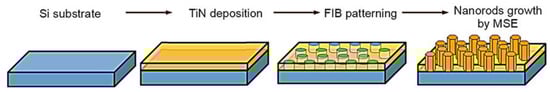
Figure 1.
Process description of the selective-area growth (SAG) of GaN nanorods (NRs) on focused ion beam lithography (FIBL) patterned substrates.
The growth of GaN NRs was performed by reactive MSE in an ultrahigh vacuum chamber by sputtering a liquid Ga (99.99999% purity) target. Details of this procedure can be found in [38]. The NRs were grown on prepatterned Si(111) substrates without removing the native oxide layer. Two sets of experiments were performed to study the growth behavior and mechanism of SAG NRs.
In the first set of experiments, the effect of process gas mixture was studied. A mixture of Ar and N2 process gas was used with different partial pressure ratios (PAr and PN₂ for argon and nitrogen, respectively) while the total chamber pressure is kept constant at 10 mTorr. The N2 partial pressures (PN₂) used in this experiment were 5, 8, 9, 9.5, and 10 mTorr for the samples named as PN₂ = 50%, 80%, 90%, 95%, and 100%, respectively. The partial pressure-dependent samples were grown for 30 min, and the growth temperature TG was kept constant at 980 °C measured from a thermocouple. An additional sample was grown in an optimized condition (PN₂ = 90%) at TG = 980 °C for 60 min to study the structural evolution of the sample.
In the second set of experiments, the effect of pitch on growth behavior was studied. A number of 5 × 5 µm2 nanohole arrays with a pitch of 100, 200, 300, and 400 nm were patterned using FIBL on a single substrate to ensure identical growth conditions for all pitches. Two growth were performed at TG = 970 °C and TG = 980 °C to simultaneously study the effect of substrate temperature on Ga adatom diffusion length (lGa) during growth. The samples were grown at PN₂ = 90% and a total pressure of 10 mTorr for 90 min.
Sample morphologies were characterized in both the top view and 45° bird’s-eye view with a Zeiss Leo 1550 field-emission gun scanning electron microscope (SEM, Zeiss, Heidenheim, Germany), operated at 10 kV. To account for the size distribution of the NRs, the diameter was calculated statistically by analyzing the plan-view SEM images with ImageJ software (version 1.52i, National Institutes of Health, Bethesda, MD, USA).
3. Results and Discussion
3.1. Effect of Gas Mixture on Nanorod Morphology and Growth Selectivity
Successful SAG of GaN nanorods depends on the preferential nucleation of GaN within the nanohole openings. The nucleation is affected by the difference of sticking coefficients, diffusion length, and desorption rate of Ga adatoms between the nanohole openings and the TiNx mask [16,39,40]. We first discuss the effects observed here of the process gas composition on the morphology of the SAG-GaN NRs.
Figure 2 shows (a) the top view and (b) the 45° bird’s-eye view SEM micrographs of the samples grown for 30 min with different percentages of N2 partial pressure. As seen in the images, the samples grown in diluted N2 (PN₂ = 50%–90%) maintain growth selectivity, with the nanorods growing only within the nanoholes. In addition, the number of NRs grown inside the openings decreases with increasing nitrogen content, indicating improved NR coalescence. Generally, increased PN₂ also results in longer NRs. For PN₂ > 90%, growth selectivity is lost, and parasitic nanorod growth occurs on the TiNx mask surface.
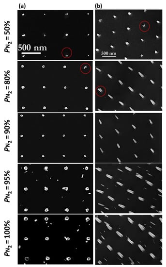
Figure 2.
(a) Top view and (b) 45° bird’s-eye view SEM micrograph of the nanorods with different PN₂ percentages. The red circles indicate where multiple nanorods grow from within a single opening.
It can be seen that individual NRs grow with slight variation in tilt angle with respect to the substrate, which may be attributed to the formation of nonuniform and locally tilted amorphous SiNx on the silicon surface, resulting in tilted NR growth [41]. For the PN₂ = 50% sample, the axial growth rate is severely affected, and a high density of uncoalesced, short NRs are formed inside the openings. The existence of multiple NRs inside a single nanohole, indicated by the red circles in Figure 2, confirms that the SAG NRs grow through the coalescence of multiple thinner nanorods, which have also been observed in MBE-based growth [42]. The growth selectivity is maintained up to PN₂ = 90%. The samples grown with PN₂ = 95% and PN₂ = 100% exhibit similar morphologies, but with parasitic growth occurring on the mask in the form of narrow NRs.
The effect of PN₂ and PAr on the SAG selectivity can be explained in terms of the Ga/N ratio on the substrate surface. Changing PN₂ and PAr directly modifies the Ga/N ratio within the chamber, affecting the availability of Ga adatoms and lGa [43,44]. Increasing PN₂ results in more active nitrogen species, lowering the Ga/N ratio. On the other hand, increasing PAr increases the sputtering yield due to the higher atomic mass of Ar and the removal of the nitride layer on the target, effectively increasing the Ga/N ratio.
The parasitic nanorod growth occurring at PN₂ > 90% corresponds to nanorods grown in low Ga/N ratio. It has been established in the MBE-based process that growth under a low Ga/N ratio results in reduced Ga adatom diffusion on the surface of the TiNx mask [15]. Because of the short lGa, parts of the Ga adatoms were unable to diffuse into the nanohole openings to nucleate as SAG NRs. In addition, the abundance of active nitrogen species increases the reaction probability between the Ga adatom and active nitrogen species on the mask surface, resulting in spontaneous NR nucleation.
As PAr is increased and PN₂ is reduced below 90%, the Ga sputtering yield increases while simultaneously the amount of active nitrogen species on the substrate surface decreases, shifting the growth condition to moderate Ga/N ratio. The selectivity improves through several mechanisms. First, lGa increases due to possible momentum transfer from the Ar ions [45]. In a MSE system, the use of high flux and low energy ions result in a transfer of momentum from ions to the adatom on the substrate surface, effectively increasing their diffusivity. The increase in lGa allows the adatoms to reach the nanoholes as the preferred nucleation sites. Second, the desorption of Ga adatoms on the mask surface increases due to reduced reaction with nitrogen, preventing the nucleation of GaN on the mask layer. From this result, we conclude that the growth selectivity of MSE-grown nanorods can be improved by increasing the amount of Ar within the process gas.
Statistical analysis was performed on the top-view SEM of the NR to calculate their diameter. Figure 3 shows the effect of PN₂ on the average diameter of the NRs. Generally, the diameter of the NRs increases with increasing nitrogen content. At high growth temperature (TG = 980 °C), the NR growth process is more sensitive to the available amount of active nitrogen species compared to lower temperature growth [46]. Under a large Ga/N ratio (low PN₂), the axial and lateral growth rate of the NRs are reduced due to the nitrogen-limited growth condition. When the radial growth rate is too low, the NRs will not coalesce, resulting in the growth of multiple individual NRs within a single opening, as shown in Figure 2. Increasing PN₂ will enhance the NR growth rate by supplying more active nitrogen species for GaN formation. In addition, active nitrogen species helps to promote the incorporation of Ga adatoms into the sidewalls, enhancing radial growth and resulting in more coalescence [15,39,47].
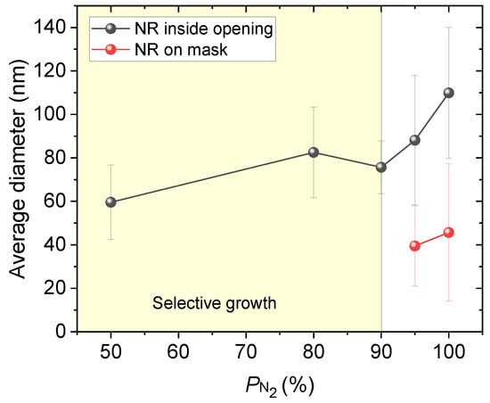
Figure 3.
Average diameters of the NRs grown inside the openings and on the mask for growth with different Ar percentage in the total process gas.
Based on the results, the growth at PN₂ = 90% and TG = 980 °C is considered to be the optimum growth condition where there is a sufficient amount of reactive N species available while the lGa is adequate for SAG growth mode. The condition promotes the coalescence of the NR nuclei, resulting in the growth of a single NR within each nanohole. Under this optimized condition, the growth is performed during 90 min to observe the evolution of the NR morphology. Based on the results shown in Figure 4, complete coalescence within the nanoholes is achieved, with no parasitic growth on the TiNx mask. The NRs show increment of both axial and radial growth. However, the high aspect ratio is maintained, indicating preferential nucleation at the c-plane facet of the nanorods, similar to self-assembled NR growth on silicon substrates [47,48].

Figure 4.
(a) Top- and (b) bird’s-eye view SEM micrographs; and (c) diameter distributions of the NRs grown at PN₂ = 90% for 90 min.
3.2. Effects of Ga Adatom Incorporation on Nanorod Growth
One of the main driving forces to form NRs has been attributed to the strong surface diffusion of adatoms at high temperature [40], which plays a vital role on the growth control of NRs. By adjusting the length between two nanoholes of the NR array (henceforth referred to as the array pitch), the effect of Ga adatom diffusion length on the NR growth behavior can be observed. The SEM micrographs for TG = 970 °C and 980 °C at various pitches are shown in Figure 5a,b, repsectively. For all pitches, no NRs nucleate on the TiNx mask, indicating that at TG = 970 and 980 °C growth selectivity is maintained.
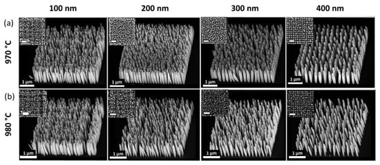
Figure 5.
Bird’s-eye view SEM micrographs of the NRs grown at (a) 970 °C and (b) 980 °C on patterns with various pitches. The inset shows the top-view SEM image of the NRs. All scale bars correspond to 1 µm.
Statistical analysis was performed to obtain the effect of pitch on the NR morphology. The average diameter of the NRs with varying pitches and grown at two different temperatures is given in Figure 6a. With increasing pitch, the diameter of the NRs increases, but the length is almost constant. For the growth performed at 980 °C, the NR diameter saturates at 300 nm pitch.
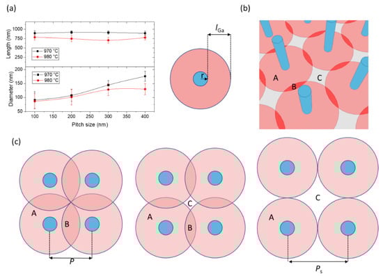
Figure 6.
(a) Average diameters and lengths of the NRs grown at TG = 970 °C and TG = 980 °C on patterns with different pitch; (b) Schematic of the GaN NR collection area model; and (c) Schematic of the pitch effect on the collection area. A, B, and C indicate the various collection zones that determine whether an incoming Ga adatom is incorporated or desorbed.
The effect of pitch on the NR morphology can be explained in terms of the Ga adatom collection area model [17,40], as depicted in Figure 6b. The collection area model concerns Ga adatoms that impinge onto both the area surrounding the NR and the adatoms that impinge directly on the NRs. It is assumed that any Ga adatoms that impinge into the substrate within a circle of radius lGa + r (with r being the radius of the NR) contribute to the growth of the NRs. This circle is indicated as zone A. Zone B is the overlap between the collection area of neighboring NRs. Adatoms impinging on zone B will be distributed evenly among the neighboring NRs. Zone C is the gap between the collection area, and adatoms impinging within this zone will be desorbed.
For both temperatures, the length of the NRs remains almost constant at different pitches while lower TG results in longer NRs. This suggests that the axial growth rate is dominated by adatoms that impinge directly on the NRs and is less dependent on the collection of Ga adatoms from the mask surface. On the other hand, for NRs grown at 980 °C, the diameter initially increased until 300 nm pitch before it saturates. The pitch where the diameter saturates is referred to as Ps. For NRs grown at 970 °C, the NR diameter continues to increase until a pitch of 400 nm.
Three different cases of pitch P are considered, as shown in Figure 6c. By modifying the equations from [40] for a rectangular lattice, we obtain the following:
- P ≤ . The entire substrate surface is covered by the NR collection zone, and zone C does not exist. All Ga adatoms impinging on the substrate surface contributes into the NR growth, and competition occurs for the Ga adatom impinging on zone B between neighboring NRs.
- ≤ P ≤ Ps. As the pitch is increased, less overlap occurs between the collection area of neighboring NRs, effectively reducing the competition for Ga adatoms between NRs. Zone C appears, and the collection zone does not cover parts of the substrate surface.
- P ≥ Ps. At the saturation pitch Ps, zone B disappears, i.e., no competition between NRs for Ga adatoms. Further increase of pitch will not affect the incorporation of Ga adatom into the NRs.
According to Gotschke et al. [40], Ps empirically corresponds to twice the diffusion length of the Ga adatom on the mask surface. However, our results suggest that at 980 °C, lGa is 150 nm, which is significantly shorter than the previously reported lGa value of 500 nm for a TiNx mask with TG = 890 °C in the case of MBE-grown GaN NRs [17]. On the other hand, at 970 °C, saturation is not yet observed at a pitch of 400 nm, which implies that the value of Ps, and consequently lGa, is longer than 200 nm at lower TG. This might seem contradictory with previously reported data [49], where an increase of TG in an MBE system corresponds to an increased Ga adatom surface diffusivity. However, this discrepancy is mainly caused by the increased desorption rate when the sample is grown at very high temperature in the desorption-dominated process regime [34,50,51], effectively decreasing the residence time of Ga adatoms on the surface. For our growth temperature, an increase in TG from 970 to 980 °C results in a net decrease of lGa as the increased desorption rate dominates over the increase in Ga adatom diffusivity.
Another consequence of increasing TG is an increased NR incubation time [17,52]. Prior to vertical growth, SAG NRs follow several incubation steps, namely the formation of a wetting layer, formation of 3D nuclei, and the coalescence of GaN islands [14]. By increasing the incubation time and delaying the onset of vertical growth, the overall NR growth rate is virtually reduced, which may contribute to the smaller NR dimension at increased temperature.
However, the reduced growth rate is mainly caused by less adatom incorporation, as evidenced by the presence of Ps at 980 °C. The decrease of lGa results in less incorporation of Ga adatoms and consequently lower radial growth. The effect of increased desorption rate also reflects a shorter residence time of Ga adatoms directly impinging on the NR top, leading to a shorter NR growth.
Based on our results, the SAG NR growth mechanism within MBE and MSE follows similar principles, mainly being driven by the effective Ga/N ratio and surface adatom diffusivity. The main difference lies in how the individual flux of Ga adatoms and active nitrogen species is regulated. In plasma-assisted MBE systems, both Ga and N flux can be adjusted individually by using separate sources, allowing more degree of freedom in determining the ratio. On the other hand, the Ga and N flux in an MSE system depends on the process gas composition and target bias, meaning their flux is coupled with each other and cannot be adjusted individually.
Qualitatively, more NR tilting is found at both very small pitch and very large pitch. Several possibilities might cause this kind of behavior. The first is the crosstalk between the nanohole openings during FIB Ga ion bombardment of the TiNx mask due to the redeposition of the mask material [30,33]. It has previously been reported that during the FIBL patterning of a nanohole pattern, several bumps consisting of redeposited Ti are found surrounding the edges of the nanoholes as a byproduct. When the pitch is small, these byproducts may get redeposited into neighboring nanohole openings, resulting in a rough surface. The second is the different Ga ion irradiation dose per unit area for different array pitches. For arrays with smaller pitch, i.e., more nanoholes, the dose per unit area will be reduced. The reduced dose can lead to incomplete milling with some mask material left inside the nanohole, resulting in a modified NR morphology [30]. On the other hand, for arrays with larger pitch, i.e., fewer nanoholes, the dose per unit area will increase. Under increased dose, substrate and mask damage may occur [53], which has been shown to result in the growth of tilted NRs [34]. Proper care on the FIBL dose per unit area and array pitch must be done to prevent crosstalk during patterning and ensure the growth of well-defined NR arrays.
4. Conclusions
We reported on the SAG process of GaN NRs by MSE on Si substrates patterned using FIBL with a thin TiNx mask layer. The effect Ar/N2 partial pressure upon the SAG growth mode of NRs is demonstrated as an important parameter to tune the effective Ga/N ratio. At PN₂ > 90%, GaN NRs nucleate both inside the nanoholes and on the mask layer, revealing low growth selectivity. By diluting the reactive gas with more Ar (PN₂ ≤ 90%), the effective Ga/N ratio on the substrate surface increases, enhancing growth selectivity. As PN₂ is further decreased to below 80%, the growth shifts to a N-limited condition, resulting in low coalescence and low axial growth rate. By growing at PN₂ = 90% and TG = 980 °C, a regular GaN NR array consisted of well-faceted single NRs with a length longer than 1 µm on FIBL-patterned Si substrates is achieved. We also studied the effect of nanohole array pitch and growth temperature on the morphology of the NRs and the quality of the NR array. We observed that the pitch of NR array affects the incorporation of Ga adatoms during NR growth due to growth competition between neighboring NRs. The surface diffusion and direct impingement of adatoms are mainly responsible for lateral and axial growth of NRs, respectively, which is well elucidated by a collection area model. A minimum pitch of 2 lGa must be used to ensure the growth of high-quality and well-defined NRs. Our work highlights the importance of a III/V ratio tuning within a MSE system for successful SAG growth of GaN nanorods.
Author Contributions
Conceptualization, E.A.S., J.B., and C.-L.H.; methodology, E.A.S., A.P., J.P., and C.-L.H.; validation, E.A.S., A.P., J.P., P.O.Å.P., L.H., J.B., and C.-L.H.; resources, J.B., L.H., P.O.Å.P., and C.-L.H.; data curation, E.A.S., A.P., and J.P.; writing—original draft preparation, E.A.S., A.P., and C.-L.H.; writing—review and editing, A.P., E.A.S., J.P., P.O.Å.P., L.H., J.B., and C.-L.H.; project administration, C.-L.H.; funding acquisition, C.-L.H., P.O.Å.P., L.H., and J.B. All authors have read and agreed to the published version of the manuscript.
Funding
This research was funded by Energimyndigheten (grant number 46658-1), Vetenskapsrådet (grant number 2018-04198), and Stiftelsen Olle Engkvist Byggmästare (grant number 197-0210), and the APC was funded by the Energimyndigheten. The Swedish Government Strategic Research Area in Materials Science on Functional Materials at Linköping University (Faculty Grant SFO-Mat-LiU 2009-00971) is acknowledged for financial support.
Conflicts of Interest
The authors declare no conflict of interest.
References
- Hu, J.; Zhang, Y.; Sun, M.; Piedra, D.; Chowdhury, N.; Palacios, T. Materials and processing issues in vertical GaN power electronics. Mater. Sci. Semicond. Process. 2018, 78, 75–84. [Google Scholar] [CrossRef]
- Ambacher, O. Growth and applications of Group III-nitrides. J. Phys. D Appl. Phys. 1998, 31, 2653–2710. [Google Scholar] [CrossRef]
- Bao, A. Group III-nitride nanowires. Mater. Sci. Technol. 2017, 33, 765–776. [Google Scholar] [CrossRef]
- Zhao, S.; Nguyen, H.P.T.; Kibria, M.G.; Mi, Z. III-Nitride nanowire optoelectronics. Prog. Quantum Electron. 2015, 44, 14–68. [Google Scholar] [CrossRef]
- Gurnett, K.; Adams, T. Native substrates for GaN: The plot thickens. III-Vs Rev. 2006, 19, 39–41. [Google Scholar] [CrossRef]
- Etzkorn, E.V.; Clarke, D.R. Cracking of GaN films. J. Appl. Phys. 2001, 89, 1025–1034. [Google Scholar] [CrossRef]
- Moram, M.A.; Ghedia, C.S.; Rao, D.V.S.; Barnard, J.S.; Zhang, Y.; Kappers, M.J.; Humphreys, C.J. On the origin of threading dislocations in GaN films. J. Appl. Phys. 2009, 106, 073513. [Google Scholar] [CrossRef]
- Kukushkin, S.A.; Osipov, A.V.; Bessolov, V.N.; Medvedev, B.K.; Nevolin, V.K.; Tcarik, K.A. Substrates for epitaxy of gallium nitride: New materials and techniques. Rev. Adv. Mater. Sci. 2008, 17, 1–32. [Google Scholar]
- Brooksby, J.C.; Mei, J.; Ponce, F.A. Correlation of spectral luminescence with threading dislocations in green-light-emitting InGaN quantum wells. Appl. Phys. Lett. 2007, 90, 231901. [Google Scholar] [CrossRef]
- Zhao, S.; Kibria, M.G.; Wang, Q.; Nguyen, H.P.T.; Mi, Z. Growth of large-scale vertically aligned GaN nanowires and their heterostructures with high uniformity on SiOx by catalyst-free molecular beam epitaxy. Nanoscale 2013, 5, 5283–5287. [Google Scholar] [CrossRef]
- Zhao, C.; Alfaraj, N.; Chandra Subedi, R.; Liang, J.W.; Alatawi, A.A.; Alhamoud, A.A.; Ebaid, M.; Alias, M.S.; Ng, T.K.; Ooi, B.S. III-nitride nanowires on unconventional substrates: From materials to optoelectronic device applications. Prog. Quantum Electron. 2018, 61, 1–31. [Google Scholar] [CrossRef]
- Lee, S.K.; Choi, H.J.; Pauzauskie, P.; Yang, P.; Cho, N.K.; Park, H.D.; Suh, E.K.; Lim, K.Y.; Lee, H.J. Gallium nitride nanowires with a metal initiated metal-organic chemical vapor deposition (MOCVD) approach. Phys. Status Solidi Basic Res. 2004, 241, 2775–2778. [Google Scholar] [CrossRef]
- Consonni, V. Self-induced growth of GaN nanowires by molecular beam epitaxy: A critical review of the formation mechanisms. Phys. Status Solidi Rapid Res. Lett. 2013, 7, 699–712. [Google Scholar] [CrossRef]
- Serban, E.A.; Palisaitis, J.; Yeh, C.-C.; Hsu, H.-C.; Tsai, Y.-L.; Kuo, H.-C.; Junaid, M.; Hultman, L.; Persson, P.O.Å.; Birch, J.; et al. Selective-area growth of single-crystal wurtzite GaN nanorods on SiOx/Si(001) substrates by reactive magnetron sputter epitaxy exhibiting single-mode lasing. Sci. Rep. 2017, 7, 12701. [Google Scholar] [CrossRef] [PubMed]
- Kishino, K.; Sekiguchi, H.; Kikuchi, A. Improved Ti-mask selective-area growth (SAG) by rf-plasma-assisted molecular beam epitaxy demonstrating extremely uniform GaN nanocolumn arrays. J. Cryst. Growth 2009, 311, 2063–2068. [Google Scholar] [CrossRef]
- Gačević, Ž.; Gómez Sánchez, D.; Calleja, E. Formation mechanisms of gan nanowires grown by selective area growth homoepitaxy. Nano Lett. 2015, 15, 1117–1121. [Google Scholar] [CrossRef]
- Schuster, F.; Hetzl, M.; Weiszer, S.; Garrido, J.A.; de la Mata, M.; Magen, C.; Arbiol, J.; Stutzmann, M. Position-controlled growth of GaN nanowires and nanotubes on diamond by molecular beam epitaxy. Nano Lett. 2015, 15, 1773–1779. [Google Scholar] [CrossRef]
- Yamano, K.; Kishino, K. Selective area growth of InGaN-based nanocolumn LED crystals on AlN/Si substrates useful for integrated μ-LED fabrication. Appl. Phys. Lett. 2018, 112, 091105. [Google Scholar] [CrossRef]
- Yanagihara, A.; Ikeda, K.; Kishino, K.; Yamano, K. Monolithic integration of four-colour InGaN-based nanocolumn LEDs. Electron. Lett. 2015, 51, 852–854. [Google Scholar]
- Kishino, K.; Nagashima, K.; Yamano, K. Monolithic integration of InGaN-Based nanocolumn light-emitting diodes with different emission colors. Appl. Phys. Express 2013, 6, 012101. [Google Scholar] [CrossRef]
- Kishino, K.; Kamimura, J.; Kamiyama, K. Near-infrared ingan nanocolumn light-emitting diodes operated at 1.46μm. Appl. Phys. Express 2012, 5, 5–8. [Google Scholar] [CrossRef]
- Kishino, K.; Ishizawa, S. Selective-area growth of GaN nanocolumns on Si(111) substrates for application to nanocolumn emitters with systematic analysis of dislocation filtering effect of nanocolumns. Nanotechnology 2015, 26, 225602. [Google Scholar] [CrossRef] [PubMed]
- Sekiguchi, H.; Kishino, K.; Kikuchi, A. Emission color control from blue to red with nanocolumn diameter of InGaN/GaN nanocolumn arrays grown on same substrate. Appl. Phys. Lett. 2010, 96, 96–99. [Google Scholar] [CrossRef]
- Ra, Y.H.; Wang, R.; Woo, S.Y.; Djavid, M.; Sadaf, S.M.; Lee, J.; Botton, G.A.; Mi, Z. Full-color single nanowire pixels for projection displays. Nano Lett. 2016, 16, 4608–4615. [Google Scholar] [CrossRef] [PubMed]
- Ra, Y.; Rashid, R.T.; Liu, X.; Sadaf, S.M.; Mashooq, K.; Mi, Z. An electrically pumped surface-emitting semiconductor green laser. Sci. Adv. 2020, 6, eaav7523. [Google Scholar] [CrossRef]
- Kouno, T.; Kishino, K.; Yamano, K.; Kikuchi, A. Two-dimensional light confinement in periodic InGaN/GaN nanocolumn arrays and optically pumped blue stimulated emission. Opt. Express 2009, 17, 20440–20447. [Google Scholar] [CrossRef]
- Ra, Y.-H.; Rashid, R.T.; Liu, X.; Lee, J.; Mi, Z. Scalable nanowire photonic crystals: Molding the light emission of InGaN. Adv. Funct. Mater. 2017, 1702364, 1702364. [Google Scholar] [CrossRef]
- Chen, Y. Nanofabrication by electron beam lithography and its applications: A review. Microelectron. Eng. 2015, 135, 57–72. [Google Scholar] [CrossRef]
- Pimpin, A.; Srituravanich, W. Reviews on micro- and nanolithography techniques and their applications. Eng. J. 2012, 16, 37–56. [Google Scholar] [CrossRef]
- Barbagini, F.; Bengoechea-Encabo, A.; Albert, S.; Martinez, J.; Sanchez García, M.A.; Trampert, A.; Calleja, E. Critical aspects of substrate nanopatterning for the ordered growth of GaN nanocolumns. Nanoscale Res. Lett. 2011, 6, 632. [Google Scholar] [CrossRef]
- Pease, R.F.; Chou, S.Y. Lithography and other patterning techniques for future electronics. Proc. IEEE 2008, 96, 248–270. [Google Scholar] [CrossRef]
- Waid, S.; Wanzenboeck, H.D.; Muehlberger, M.; Gavagnin, M.; Bertagnolli, E. Focused ion beam direct patterning of hardmask layers. J. Vac. Sci. Technol. B Microelectron. Nanom. Struct. 2014, 32, 041602. [Google Scholar] [CrossRef]
- Martinez, J.; Barbagini, F.; Bengoechea-Encabo, A.; Albert, S.; Sanchez García, M.A.; Calleja, E. Fabrication of GaN nanorods by focused ion beam. Microelectron. Eng. 2012, 98, 250–253. [Google Scholar] [CrossRef][Green Version]
- Serban, E.A.; Palisaitis, J.; Persson, P.O.Å.; Hultman, L.; Birch, J.; Hsiao, C.L. Site-controlled growth of GaN nanorod arrays by magnetron sputter epitaxy. Thin Solid Films 2018, 660, 950–955. [Google Scholar] [CrossRef]
- Prabaswara, A.; Birch, J.; Junaid, M.; Serban, E.A.; Hultman, L.; Hsiao, C.-L. Review of GaN thin film and nanorod growth using magnetron sputter epitaxy. Appl. Sci. 2020, 10, 3050. [Google Scholar] [CrossRef]
- Izyumskaya, N.; Avrutin, V.; Ding, K.; Ozgur, U.; Morkoc, H.; Fujioka, H. Emergence of high quality sputtered III-nitride semiconductors and devices. Semicond. Sci. Technol. 2019. [Google Scholar] [CrossRef]
- Junaid, M.; Hsiao, C.; Chen, Y.-T.; Lu, J.; Palisaitis, J.; Persson, P.O.Å.; Hultman, L.; Birch, J. Effects of N2 partial pressure on growth, structure, and optical properties of GaN nanorods deposited by liquid-target reactive magnetron sputter epitaxy. Nanomaterials 2018, 8, 223. [Google Scholar] [CrossRef]
- Junaid, M.; Hsiao, C.-L.; Palisaitis, J.; Jensen, J.; Persson, P.O.Å.; Hultman, L.; Birch, J. Electronic-grade GaN(0001)/Al2O3(0001) grown by reactive DC-magnetron sputter epitaxy using a liquid Ga target. Appl. Phys. Lett. 2011, 98, 141915. [Google Scholar] [CrossRef]
- Bengoechea-Encabo, A.; Barbagini, F.; Fernandez-Garrido, S.; Grandal, J.; Ristic, J.; Sanchez-Garcia, M.A.; Calleja, E.; Jahn, U.; Luna, E.; Trampert, A. Understanding the selective area growth of GaN nanocolumns by MBE using Ti nanomasks. J. Cryst. Growth 2011, 325, 89–92. [Google Scholar] [CrossRef]
- Gotschke, T.; Schumann, T.; Limbach, F.; Stoica, T.; Calarco, R. Influence of the adatom diffusion on selective growth of GaN nanowire regular arrays. Appl. Phys. Lett. 2011, 98, 103102. [Google Scholar] [CrossRef]
- Stoica, T.; Sutter, E.; Meijers, R.J.; Debnath, R.K.; Calarco, R.; Lüth, H.; Grützmacher, D. Interface and wetting layer effect on the catalyst-free nucleation and growth of gan nanowires. Small 2008, 4, 751–754. [Google Scholar] [CrossRef] [PubMed]
- Schumann, T.; Gotschke, T.; Limbach, F.; Stoica, T.; Calarco, R. Selective-area catalyst-free MBE growth of GaN nanowires using a patterned oxide layer. Nanotechnology 2011, 22, 095603. [Google Scholar] [CrossRef] [PubMed]
- Shinoda, H.; Mutsukura, N. Structural properties of GaN and related alloys grown by radio-frequency magnetron sputter epitaxy. Thin Solid Film. 2008, 516, 2837–2842. [Google Scholar] [CrossRef]
- Steib, F.; Remmele, T.; Gülink, J.; Fündling, S.; Behres, A.; Wehmann, H.-H.; Albrecht, M.; Straßburg, M.; Lugauer, H.-J.; Waag, A. Defect generation by nitrogen during pulsed sputter deposition of GaN. J. Appl. Phys. 2018, 124, 175701. [Google Scholar] [CrossRef]
- Greczynski, G.; Lu, J.; Jensen, J.; Bolz, S.; Kölker, W.; Schiffers, C.; Lemmer, O.; Greene, J.E.; Hultman, L. A review of metal-ion-flux-controlled growth of metastable TiAlN by HIPIMS/DCMS co-sputtering. Surf. Coat. Technol. 2014, 257, 15–25. [Google Scholar] [CrossRef]
- Bertness, K.A.; Sanders, A.W.; Rourke, D.M.; Harvey, T.E.; Roshko, A.; Schlager, J.B.; Sanford, N.A. Controlled nucleation of GaN nanowires grown with molecular beam epitaxy. Adv. Funct. Mater. 2010, 20, 2911–2915. [Google Scholar] [CrossRef]
- Lymperakis, L.; Neugebauer, J. Large anisotropic adatom kinetics on nonpolar GaN surfaces: Consequences for surface morphologies and nanowire growth. Phys. Rev. B 2009, 79, 241308. [Google Scholar] [CrossRef]
- Calarco, R.; Meijers, R.J.; Debnath, R.K.; Stoica, T.; Sutter, E.; Lüth, H. Nucleation and growth of GaN nanowires on Si(111) performed by molecular beam epitaxy. Nano Lett. 2007, 7, 2248–2251. [Google Scholar] [CrossRef]
- Songmuang, R.; Landré, O.; Daudin, B. From nucleation to growth of catalyst-free GaN nanowires on thin AlN buffer layer. Appl. Phys. Lett. 2007, 91, 251902. [Google Scholar] [CrossRef]
- Consonni, V.; Dubrovskii, V.G.; Trampert, A.; Geelhaar, L.; Riechert, H. Quantitative description for the growth rate of self-induced GaN nanowires. Phys. Rev. B 2012, 85, 155313. [Google Scholar] [CrossRef]
- Fernández-Garrido, S.; Grandal, J.; Calleja, E.; Sánchez-García, M.A.; López-Romero, D. A growth diagram for plasma-assisted molecular beam epitaxy of GaN nanocolumns on Si(111). J. Appl. Phys. 2009, 106, 2007–2010. [Google Scholar] [CrossRef]
- Morassi, M.; Guan, N.; Dubrovskii, V.G.; Berdnikov, Y.; Barbier, C.; Mancini, L.; Largeau, L.; Babichev, A.V.; Kumaresan, V.; Julien, F.H.; et al. Selective area growth of GaN nanowires on graphene nanodots. Cryst. Growth Des. 2020, 20, 552–559. [Google Scholar] [CrossRef]
- Gierak, J.; Bourhis, E.; Jede, R.; Bruchhaus, L.; Beaumont, B.; Gibart, P. FIB technology applied to the improvement of the crystal quality of GaN and to the fabrication of organised arrays of quantum dots. Microelectron. Eng. 2004, 73–74, 610–614. [Google Scholar] [CrossRef]
© 2020 by the authors. Licensee MDPI, Basel, Switzerland. This article is an open access article distributed under the terms and conditions of the Creative Commons Attribution (CC BY) license (http://creativecommons.org/licenses/by/4.0/).