Abstract
This study is based on the film growth by non-classical crystallization, where charged nanoparticles (NPs) are the building block of film deposition. Extensive studies about the generation of charged NPs and their contribution to film deposition have been made in the chemical vapor deposition (CVD) process. However, only a few studies have been made in the physical vapor deposition (PVD) process. Here, the possibility for Ti films to grow by charged Ti NPs was studied during radio frequency (RF) sputtering using Ti target. After the generation of charged Ti NPs was confirmed, their influence on the film quality was investigated. Charged Ti NPs were captured on amorphous carbon membranes with the electric bias of −70 V, 0 V, +5 V, +15 V and +30 V and examined by transmission electron microscopy (TEM). The number density of the Ti NPs decreased with increasing positive bias, which showed that some of Ti NPs were positively charged and repelled by the positively biased TEM membrane. Ti films were deposited on Si substrates with the bias of −70 V, 0 V and +30 V and analyzed by TEM, field-emission scanning electron microscopy (FESEM), X-ray diffraction (XRD) and X-ray reflectivity (XRR). The film deposited at −70 V had the highest thickness of 180 nm, calculated density of 4.974 g/cm3 and crystallinity, whereas the film deposited at +30 V had the lowest thickness of 92 nm, calculated density of 3.499 g/cm3 and crystallinity. This was attributed to the attraction of positively charged Ti NPs to the substrate at −70 V and to the landing of only small-sized neutral Ti NPs on the substrate at +30 V. These results indicate that the control of charged NPs is necessary to obtain a high quality thin film at room temperature.
1. Introduction
Ti thin films are widely used in biomedical applications [,,] and microelectronics [,] because of their outstanding properties such as good biocompatibility, excellent thermal and chemical stability []. Ti films are broadly prepared using various sputtering such as direct current (DC) sputtering [,,,,], radio frequency (RF) sputtering [], high power impulse magnetron sputtering (HiPIMS) [,,], which is a well-established technique in industry to deposit thin films with high reproducibility and growth rate.
Meanwhile, the deposition process of thin films has been based on understanding that thin films grow by the building block of atoms, ions and molecules. However, there have been several puzzling phenomena that cannot be explained by such a classical crystallization mechanism. Recently, many researchers have reported an experimental evidence that many crystals including thin films grow by the building block of nanoparticles (NPs), which has been called ‘non-classical crystallization’ [,,,,,,,].
Hwang et al. [] have extensively studied non-classical crystallization in a chemical vapor deposition (CVD) system. They suggest that NPs having an electric charge are spontaneously generated in the gas phase in a conventional CVD process and become the building block of thin films. The charge carried by NPs plays an important role in the deposition of crystalline thin films [,,] and in the synthesis of nanostructures such as nanorod [] and tetrapod []. They called this new thin film growth mechanism ‘theory of charged NPs (TCN)’. According to TCN, neutral NPs tend to form a porous structure by random Brownian coagulation, whereas charged NPs tend to produce a dense film, resulting from the orderly manner of deposition by self-assembly. In the gas phase, neutral NPs tend to be amorphous whereas charged NPs tend to be crystalline, implying that atoms in charged NPs are much more mobile than those in neutral NPs. On landing on the surface, charged NPs undergo liquid-like coalescence or epitaxial recrystallization and result in dense and crystalline structures. The high atomic mobility of charged NPs and their liquid-like coalescence imply that the bond strength of NPs might be weakened by the charge. Indeed, by the ab initio calculation Clare et al. [] reported that the bond strength of Si-H and Si-Si is weakened by the presence of positive or negative charge in silane (SiH4) and disilane (Si2H6) molecules. Also, these aspects of TCN have been demonstrated experimentally in many CVD systems []. For instance, a homoepitaxial Si film on the Si substrate was deposited by applying the negative substrate bias at a low substrate temperature of 550 °C during plasma enhanced CVD [] and a highly crystalline and dense Si film was obtained by controlling the behavior of Si charged NPs during inductively coupled plasma CVD [].
Only a few studies have been made for the possibility of the generation of NPs in the gas phase in a physical vapor deposition (PVD) process. Sahu et al. [] enhanced the properties of indium tin oxide (ITO) films by inducing the generation of crystalline NPs during a modified RF sputtering system with 3-dimensionally (3-D) confined magnetron source. Hayasaki et al. [] also obtained epitaxial yttrium barium copper oxide (YBa2CuO7-x) films using nano-sized clusters during thermal plasma flash evaporation. However, these studies did not concern the presence and the role of the charge of NPs.
In this paper, as a first step to check the possibility that Ti films also grow by charged Ti NPs in the RF sputtering system using a Ti target, the generation of charged Ti NPs was studied. The generation of Ti NPs and their polarity were confirmed by applying the electric bias to amorphous carbon membranes for transmission electron microscopy (TEM). The effect of charged Ti NPs on the film deposition was examined by applying the electric bias to the p-type Si (100) substrate. Characteristics of the Ti NPs and films were analyzed by TEM, field-emission scanning electron microscopy (FESEM), X-ray diffraction (XRD) and X-ray reflectivity (XRR).
2. Materials and Methods
Figure 1a shows schematics of the RF sputtering system using a Ti target. The distance between the Ti target and a sample stage was 7 cm. An amorphous carbon TEM membrane (Ted Pella, Inc., Redding, CA, USA) for capturing NPs or a p-type Si substrate for film deposition was placed on a steel plate, which was electrically isolated from the grounded sample stage in order to apply the electric bias on the steel plate. A grounded mesh in Figure 1b was installed 2 mm above the steel plate to prevent the electric bias of the steel plate from interfering with the plasma condition. For this prevention, the hole size of the grounded mesh was selected less than Debye length []. The electric field generated between the grounded mesh and steel plate would interact with charged NPs. A round-shaped shutter with 5 cm diameter was installed 5 mm above the grounded mesh in order to control the exposure time for capturing NPs or the deposition of film. In other words, the plasma flux was blocked when the shutter was closed, and the capturing or deposition started shortly after the shutter opened.
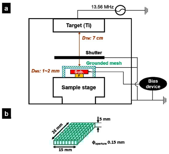
Figure 1.
Schematics of RF sputtering system (a) main chamber (b) grounded mesh.
Ar gas pressure, RF power and substrate temperature were 20 mTorr, 160 W and room temperature, respectively, for all experiments. All parameters are commonly used in the researches of sputtering system [,,]. To confirm the existence of Ti charged NPs, the Ti NPs were captured on the TEM membrane for 30 s at various electric biases of −70 V, 0 V, +5 V, +15 V and +30 V. Also, to confirm the effect of Ti charged NPs on the actual deposition process, Ti thin films were deposited on Si substrates for 30 min at −70 V, 0 V and +30 V under the same condition as capturing NPs.
To stabilize the plasma condition, the capturing NPs and film deposition processes were conducted 30 s after the plasma is turned on. During this stabilizing time of 30 s, the TEM membrane and the Si substrate were screened from the plasma by the shutter.
The captured Ti charged NPs were analyzed by TEM (FEI, Tecnai F20, Hillsboro, OR, USA). The microstructure of the Ti films was investigated by FESEM (Carl Zeiss, SUPRA, Oberkochen, Germany) and TEM. FESEM and TEM were operated at accelerating voltages of 2 kV and 200 kV, respectively. The crystallinity and density of the films were analyzed, respectively, by XRD (PANalytical, X’pert-Pro, Almelo, The Netherlands) and XRR (PANalytical, X’pert-pro). Using Cu-Kα wavelength of 0.154 nm, XRD and XRR were measured at 2-theta ranges of 20° ~ 60° and 0° ~ 0.7°, respectively.
3. Results and Discussion
3.1. Capturing Charged NPs during RF Sputtering with a Ti Target
Charged NPs, if any, were expected to interact with the electric field generated between the grounded mesh and the steel plate. In Figure 2, scanning transmission electron microscope (STEM) images show the white dots, which are confirmed to be titanium dioxide (TiO2) NPs in Figure 3, captured for 30 s at various steel plate biases of −70 V, 0 V, +5 V, +15 V and +30 V. As shown in Figure 2, the number density of NPs increased by increasing the negative bias from 0 V to −70 V. In contrast, it decreased by increasing the positive bias from 0 V to +30 V. It indicates that the NPs were positively charged since they would be attracted to the TEM membrane when the negative bias was applied and repelled when the positive bias was applied. For example, if +30 V is applied, positively charged NPs having energy less than 30 eV would be repelled. Therefore, the higher positive bias was applied, the more positively charged NPs would be repelled considering the energy distribution of charged NPs.
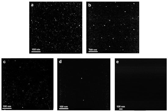
Figure 2.
STEM images of NPs captured on amorphous carbon TEM membranes at the electric biases of (a) −70 V (b) 0 V (c) +5 V (d) +15 V and (e) +30 V.
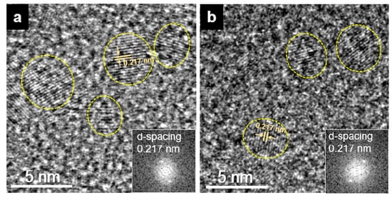
Figure 3.
HRTEM images and FFT information (inset of the lower right in the image) with d-spacing value of NPs at the electric biases of (a) −70 V and (b) 0 V.
NPs were not observed on the TEM membrane at +30 V as shown in Figure 2e. All positively charged NPs are expected to be repelled. On the other hand, negatively charged species like electrons are expected to be blocked by the grounded mesh due to the potential difference between the plasma and the grounded mesh. The grounded mesh has a more negative potential with respect to plasma since plasma has always the most positive potential in the chamber. Therefore, any negatively charged particle that does not have enough energy to overcome the potential difference between the plasma and the grounded mesh could not come to the TEM membrane through the grounded mesh. Thus, negatively charged NPs passing through the grounded mesh are expected to be hardly observed on the TEM membrane.
There are two possibilities as to the absence of NPs on the TEM membrane at +30 V. One possibility is that there were no neutral NPs that came to the TEM membrane since neutral NPs should be observed regardless of the sign of the applied bias. The other possibility is that neutral NPs landed on the TEM membrane but could not be observed because of their too small size to be detected by high-resolution transmission electron microscopy (HRTEM). To ascertain these two possibilities, Ti thin films were deposited for a longer time under the same conditions as capturing the charged NPs, which will be discussed in Section 3.2.
Figure 3 shows HRTEM images and fast Fourier transform (FFT) information of the NPs captured at −70 V and 0 V. The majority of the captured NPs as marked by circles in the images had the average size of ~5 nm and d-spacing of ~0.217 nm, indicating that the NPs were TiO2 with the (220) crystal plane. This would be because Ti becomes oxidized easily. Ti NPs might turn into TiO2 NPs immediately after they were taken out of the vacuum chamber and exposed to air [,].
3.2. Ti Thin Film Deposition
Ti films were deposited on Si substrates for 30 min under the condition where the biases of −70 V, 0 V and +30 V were applied to the steel plate substrate holder. Cross-section SEM images of these films are shown in Figure 4. Compared to the Ti film deposited at 0 V, a thicker film was obtained at −70 V, whereas a thinner film was obtained at +30 V. This result agrees with the observation that the sign of most charged Ti NPs is positive as shown in Figure 2.
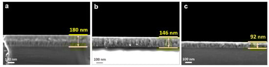
Figure 4.
SEM images of the Ti films deposited on Si substrates at the electric biases of (a) −70 V (b) 0 V and (c) +30 V.
In the case of +30 V, a 92 nm thick Ti film was deposited although no NPs were observed as shown in Figure 2e. If neutral NPs did not exist, the Ti film would be deposited only by neutral atoms and should have the highest crystallinity and density under the bias condition of +30 V. On the other hand, if neutral NPs were not observed because of their invisibly small size as discussed above, the Ti film would be deposited by the invisibly small neutral Ti NPs as well as atoms and should have low crystallinity and density. The invisibly small NPs might be more appropriately called clusters. Jeon et al. [] reported that the film deposited by a high fraction of neutral clusters showed a rough surface morphology with a porous structure whereas the film deposited by a high fraction of charged clusters showed a smooth morphology with a dense structure during thermal evaporation of copper. Therefore, it is necessary to analyze the crystallinity and density of films deposited at −70 V, 0 V and +30 V to distinguish whether the film grows mainly by neutral atoms or clusters.
Figure 5 shows XRD data of the films deposited at −70 V, 0 V and +30 V. In Figure 5, the films deposited at −70 V and 0 V mainly showed XRD peaks with (100) and (002) orientations of Ti, respectively. The different orientations of the deposited films would have come from the different incident energy of sputtered species into each substrate. Kwon et al. [] stated that different incident energy of positively charged NPs affected the microstructure of the deposited films on floating and grounded substrates during Ti RF sputtering. According to the results of Kwon et al., Ti films tended to grow in the (100) orientation when the incident energy of positively charged NPs was high, but grew in the (002) orientation when their incident energy was low. In this experiment, at −70 V and 0 V, positively charged NPs could be incident into the substrate after they passed through the grounded mesh. In the case of −70 V, the positively charged NPs would be accelerated by the substrate bias when they came into the substrate after passing through the grounded mesh. Therefore, their incident energy was relatively high, and the film was expected to grow in the (100) orientation. On the other hand, in the case of 0 V, the positively charged NPs would not be accelerated by the substrate bias since the electrical potential of the substrate and the grounded mesh was the same. Here, their incident energy was relatively low, and the film was expected to grow in the (002) orientation. However, the film deposited at +30 V did not show any clear XRD peak, which indicates that the film had a high fraction of an amorphous phase or nano-sized crystallites. This result implies that not only neutral atoms but also neutral clusters contributed to the growth of the film deposited at +30 V.
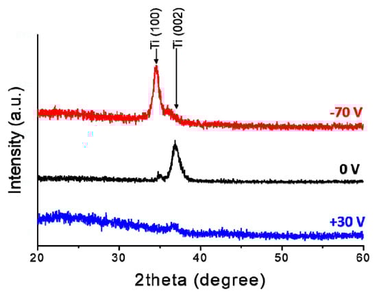
Figure 5.
XRD data of the Ti films deposited at the electric biases of −70 V, 0 V and +30 V.
This possibility is further supported by Figure 6a–f, which show respectively low and high magnification HRTEM images of the films deposited at −70 V, 0 V and +30 V. In Figure 6d–f, the films deposited at −70 V and 0 V show lattice fringe images of the higher contrast and more ordered shaped FFT images in the right bottom inset than that deposited at +30 V. The film deposited at +30 V shows blurred lattice fringes as marked by the ovals in Figure 6f.
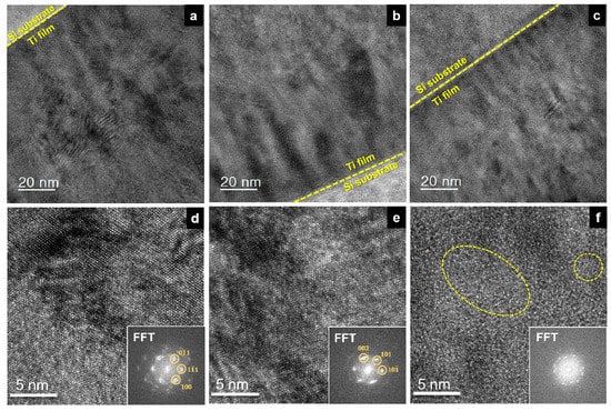
Figure 6.
HRTEM images of (a–c) low magnification and (d–f) high magnification with FFT information of the Ti films deposited on Si substrates at the electric biases of (a), (d) −70 V (b), (e) 0 V and (c), (f) +30 V.
Moreover, as shown in Figure 7a–c, diffraction pattern images show that the films deposited at −70 V and 0 V had clear diffraction patterns, whereas that deposited at +30 V had an obscure and scattered pattern. Considering the analysis of XRD, HRTEM and diffraction pattern images, it can be concluded that the films deposited at −70 V and 0 V had higher crystallinity than that deposited at +30 V. Therefore, as mentioned above, it is highly probable that the film deposited at +30 V should grow not only by neutral atoms but also by neutral clusters. To verify this possibility further, the density of the films was analyzed.
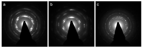
Figure 7.
Diffraction pattern images of the Ti films at the electric biases of (a) −70 V (b) 0 V and (c) +30 V.
Figure 8 corresponds to the first 0.7 degrees of XRR graphs of the films deposited at −70 V, 0 V and +30 V, which show the critical angle of the films at the inflection point of the graphs. The critical angle of the films deposited at −70 V, 0 V and +30 V were 0.31°, 0.28° and 0.25°, respectively. The density of the film was theoretically calculated using the following equation,
where αc is the critical angle, r0 is the classical electron radius, λ is the wavelength of CuKα1, NA is Avogadro’s number, Z is the atomic number of Ti, f′ is the real part of the dispersion coefficient, A is the atomic weight of Ti and ρ is the density of the films []. Theoretically calculated densities of films deposited at −70 V, 0 V and +30 V were 4.974, 4.058 and 3.499 g/cm3, respectively.
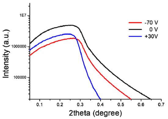
Figure 8.
XRR data of the Ti films in the range of 0°~0.7° at the electric biases of −70 V, 0 V and +30 V.
Table 1 shows the summarized characteristics of the films. It is noted that the film deposited at +30 V showed the lowest crystallinity and density. Considering these results, it is confirmed that the deposition of the film at +30 V was contributed by not only neutral atoms but also neutral clusters. Therefore, the small neutral NPs were expected to land on the substrate although they were not observed by TEM due to their small size. Neutral atoms would also deposit on the substrate, but it seems that they did not significantly improve the film quality. If the film at +30 V was deposited solely atom by atom, it should have an extraordinarily high crystallinity and density, which may exceed the properties of the films deposited at −70 V and 0 V.

Table 1.
Characteristics of the Ti films with thickness, crystallinity, the calculated density and the measured critical angle by XRR at the electric bias of −70 V, 0 V and +30 V.
However, the high crystallinity and density of the film deposited at −70 V were attributed mainly to the positively charged NPs. When the positively charged NPs came down through the grounded mesh, they were accelerated toward the negatively biased substrate and consequently formed a dense film.
Furthermore, the liquid-like property of the positively charged NPs could play an important role in forming crystalline and dense films. According to the result of Jung et al. [], the charge carried by NPs weakens the bond strength of NPs and makes the NPs ‘liquid-like’. Using the liquid-like property of charged NPs, they produced a homoepitaxial silicon film using hot-wire CVD. Youn et al. [] also emphasized the critical role of the charge carried by NPs in the formation of crystalline silicon nanowires and dense silicon films using CVD. This explanation that the charge weakens the bond strength is supported by the ab initio calculation. []
Similarly, due to the acceleration of the positively charged NPs to the substrate by the bias of −70 V, the film deposited at −70 V has better crystallinity and higher density than those deposited at 0 V and +30 V. Therefore, charged NPs played an important role in growing the highly crystalline and dense film at room temperature in the RF sputtering process.
4. Conclusions
This study investigated the effect of charged NPs on the film growth in PVD process based on non-classical crystallization. Charged Ti NPs were spontaneously generated during RF sputtering and their deposition behavior was affected by the substrate bias. Positively charged Ti NPs were captured on amorphous carbon membranes at various substrate biases and analyzed by TEM. The Ti film deposited at −70 V had the highest thickness, crystallinity and density whereas the Ti film deposited at +30 V had the lowest ones. Based on these results, it is suggested that charged NPs produce films of higher crystallinity and density than neutral NPs in PVD process.
Author Contributions
Conceptualization, J.-H.K. and N.-M.H.; methodology, J.-H.K. and D.-Y.K.; formal analysis, J.-H.K. and D.-Y.K.; investigation, J.-H.K. and D.-Y.K.; data curation, J.-H.K. and D.-Y.K.; writing—original draft preparation, J.-H.K. and D.-Y.K.; writing—review and editing, N.-M.H.; supervision, N.-M.H. All authors have read and agreed to the published version of the manuscript.
Funding
This work was supported by Global Frontier Program through the Global Frontier Hybrid Interface Materials (GFHIM) of the National Research Foundation of Korea (NRF) funded by the Ministry of Science, ICT & Future Planning (MSIT) (No. NRF-2013M3A6B1078874) and the National Research Foundation of Korea (NRF) grant funded by the Korea government (MSIT) (No. 2020R1A5A6017701).
Conflicts of Interest
The authors declare no conflict of interest.
References
- Boyer, R. An overview on the use of titanium in the aerospace industry. Mater. Sci. Eng. A 1996, 213, 103–114. [Google Scholar] [CrossRef]
- Elias, C.N.; Lima, J.H.C.; Valiev, R.; Meyers, M.A. Biomedical applications of titanium and its alloys. JOM 2008, 60, 46–49. [Google Scholar] [CrossRef]
- Kaur, M.; Singh, K. Review on titanium and titanium based alloys as biomaterials for orthopaedic applications. Mater. Sci. Eng. C 2019, 102, 844–862. [Google Scholar] [CrossRef] [PubMed]
- Huang, L.; Liu, B.; Zhu, Q.; Chen, S.; Gao, M.; Qin, F.; Wang, D. Low resistance Ti Ohmic contacts to 4H-SiC by reducing barrier heights without high temperature annealing. Appl. Phys. Lett. 2012, 100, 263503. [Google Scholar] [CrossRef]
- Suzuki, M.; Kawakami, T.; Arai, T.; Kobayashi, S.; Koide, Y.; Uemura, T.; Shibata, N.; Murakami, M. Low-resistance Ta/Ti Ohmic contacts for p-type GaN. Appl. Phys. Lett. 1999, 74, 275–277. [Google Scholar] [CrossRef]
- Ting, C.; Wittmer, M. The use of titanium-based contact barrier layers in silicon technology. Thin Solid Film. 1982, 96, 327–345. [Google Scholar] [CrossRef]
- Chawla, V.; Jayaganthan, R.; Chawla, A.K.; Chandra, R. Morphological study of magnetron sputtered Ti thin films on silicon substrate. Mater. Chem. Phys. 2008, 111, 414–418. [Google Scholar] [CrossRef]
- Chawla, V.; Jayaganthan, R.; Chawla, A.K.; Chandra, R. Microstructural characterizations of magnetron sputtered Ti films on glass substrate. J. Mater. Process. Technol. 2009, 209, 3444–3451. [Google Scholar] [CrossRef]
- Chen, A.Y.; Bu, Y.; Tang, Y.; Wang, Y.; Liu, F.; Xie, X.; Gu, J.; Pan, D. Deposition-rate dependence of orientation growth and crystallization of Ti thin films prepared by magnetron sputtering. Thin Solid Film. 2015, 574, 71–77. [Google Scholar] [CrossRef]
- Jeyachandran, Y.L.; Karunagaran, B.; Narayandass, S.; Mangalaraj, D. The effect of thickness on the properties of titanium films deposited by dc magnetron sputtering. Mater. Sci. Eng. A 2007, 458, 361–365. [Google Scholar] [CrossRef]
- Miyoshi, T.; Haga, Y.; Nittono, O. Microstructure and preferred orientation in pure titanium films deposited by two-facing-target-type DC sputtering. Thin Solid Film. 1996, 281, 128–131. [Google Scholar] [CrossRef]
- Muslim, N.; Soon, Y.W.; Lim, C.M.; Voo, Y.N. Influence of sputtering power on properties of titanium thin films deposited by RF magnetron sputtering. ARPN J. Eng. Appl. Sci. 2015, 10, 7148–7189. [Google Scholar]
- Audronis, M.; Bellido-Gonzalez, V. The effect of Ti sputter target oxidation level on reactive High Power Impulse Magnetron Sputtering process behaviour. Surf. Coat. Technol. 2011, 205, S322–S325. [Google Scholar] [CrossRef]
- Wu, B.; Yu, Y.; Wu, J.; Shchelkanov, I.; Ruzic, D.N.; Huang, N.; Leng, Y. Tailoring of titanium thin film properties in high power pulsed magnetron sputtering. Vacuum 2018, 150, 144–154. [Google Scholar] [CrossRef]
- Ghasemi, S.; Seyfi, P.; Farhadizadeh, A.; Ghomi, H. The experimental approach into the influence of external inductance on the discharge characteristic of HiPIMS. J. Theor. Appl. Phys. 2019, 13, 289–297. [Google Scholar] [CrossRef]
- Aizenberg, J.; Braun, P.V.; Wiltzius, P. Patterned colloidal deposition controlled by electrostatic and capillary forces. Phys. Rev. Lett. 2000, 84, 2997–3000. [Google Scholar] [CrossRef]
- Demortière, A.; Snezhko, A.; Sapozhnikov, M.V.; Becker, N.; Proslier, T.; Aranson, I.S. Self-assembled tunable networks of sticky colloidal particles. Nat. Commun. 2014, 5, 3117. [Google Scholar] [CrossRef]
- Ferrar, J.A.; Solomon, M.J. Kinetics of colloidal deposition, assembly, and crystallization in steady electric fields. Soft Matter 2015, 11, 3599–3611. [Google Scholar] [CrossRef]
- Sadri, B.; Pernitsky, D.J.; Sadrzadeh, M. Aggregation and deposition of colloidal particles: Effect of surface properties of collector beads. Colloids Surf. A Physicochem. Eng. Asp. 2017, 530, 46–52. [Google Scholar] [CrossRef]
- Wang, Z.; He, B.; Xu, G.; Wang, G.; Wang, J.; Feng, Y.; Su, D.; Chen, B.; Li, H.; Wu, Z.; et al. Transformable masks for colloidal nanosynthesis. Nat. Commun. 2018, 9, 563. [Google Scholar] [CrossRef]
- Kim, D.-S.; Hwang, N.-M. Synthesis of nanostructures using charged nanoparticles spontaneously generated in the gas phase during chemical vapor deposition. J. Phys. D Appl. Phys. 2018, 51, 463002. [Google Scholar] [CrossRef]
- Kim, C.-S.; Chung, Y.-B.; Youn, W.-K.; Hwang, N.-M. Generation of charged nanoparticles during synthesis of ZnO nanowires by carbothermal reduction. Aerosol Sci. Technol. 2009, 43, 120–125. [Google Scholar] [CrossRef]
- Hwang, N.M. Non-Classical Crystallization of Thin Films and Nanostructures in CVD and PVD Processes; Springer Netherlands: Dordrecht, The Netherlands, 2016; Volume 60, pp. 1–332. ISBN 978-94-017-7616-5. [Google Scholar]
- Jung, J.-S.; Lee, S.-H.; Kim, D.-S.; Kim, K.-S.; Park, S.-W.; Hwang, N.-M. Non-classical crystallization of silicon thin films during hot wire chemical vapor deposition. J. Cryst. Growth 2017, 458, 8–15. [Google Scholar] [CrossRef]
- Youn, W.-K.; Lee, S.-S.; Lee, J.-Y.; Kim, C.-S.; Hwang, N.-M.; Iijima, S. Comparison of the deposition behavior of charged silicon nanoparticles between floating and grounded substrates. J. Phys. Chem. C 2014, 118, 11946–11953. [Google Scholar] [CrossRef]
- Jeon, I.-D.; Barnes, M.; Kim, D.-Y.; Hwang, N.M. Origin of positive charging of nanometer-sized clusters generated during thermal evaporation of copper. J. Cryst. Growth 2003, 247, 623–630. [Google Scholar] [CrossRef]
- Park, S.-H.; Park, J.-W.; Yang, S.-M.; Kim, K.-H.; Hwang, N.-M. Effect of electric bias on the deposition behavior of ZnO nanostructures in the chemical vapor deposition process. J. Phys. Chem. C 2015, 119, 25047–25052. [Google Scholar] [CrossRef]
- Clare, B.W.; Talukder, G.; Jennings, P.J.; Cornish, J.C.L.; Hefter, G. Effect of charge on bond strength in hydrogenated amorphous silicon. J. Comput. Chem. 1994, 15, 644–652. [Google Scholar] [CrossRef]
- Park, S.-W.; Jung, J.-S.; Kim, K.-S.; Kim, K.-H.; Hwang, N.-M. Effect of bias applied to the substrate on the low temperature growth of silicon epitaxial films during RF-PECVD. Cryst. Growth Des. 2018, 18, 5816–5823. [Google Scholar] [CrossRef]
- Yoo, S.-W.; You, S.J.; Kim, J.-H.; Seong, D.-J.; Seo, B.-H.; Hwang, N.-M. Effect of substrate bias on deposition behaviour of charged silicon nanoparticles in ICP-CVD process. J. Phys. D Appl. Phys. 2016, 50, 35201. [Google Scholar] [CrossRef]
- Sahu, B.B.; Long, W.; Han, J.G. Highly conductive flexible ultra thin ITO nanoclusters prepared by 3-D confined magnetron sputtering at a low temperature. Scr. Mater. 2018, 149, 98–102. [Google Scholar] [CrossRef]
- Hayasaki, K.; Terashima, K.; Yoshida, T.; Takamura, Y.; Yamaguchi, N. Scanning tunneling microscopy of epitaxial YBa2Cu3O7−x films prepared by thermal plasma flash evaporation method. J. Appl. Phys. 1997, 81, 1222–1226. [Google Scholar] [CrossRef]
- Chapman, B.N. Glow Discharge Processes: Sputtering and Plasma Etching; Wiley: New York, NY, USA, 1980; pp. 1–406. ISBN 978-04-710-7828-9. [Google Scholar]
- Briot, O.; Moret, M.; Barbier, C.; Tiberj, A.; Peyre, H.; Sagna, A.; Contreras, S. Optimization of the properties of the molybdenum back contact deposited by radiofrequency sputtering for Cu(In1−xGax) Se2 solar cells. Sol. Energy Mater. Sol. Cells 2018, 174, 418–422. [Google Scholar] [CrossRef]
- Kampylafka, V.; Kostopoulos, A.; Modreanu, M.; Schmidt, M.; Gagaoudakis, E.; Tsagaraki, K.; Kontomitrou, V.; Konstantinidis, G.; Deligeorgis, G.; Kiriakidis, G.; et al. Long-term stability of transparent n/p ZnO homojunctions grown by rf-sputtering at room-temperature. J. Mater. 2019, 5, 428–435. [Google Scholar] [CrossRef]
- Acosta, M.; Méndez, R.A.; Riech, I.; Rodríguez-Pérez, M.; Rodríguez-Gattorno, G. Structural, optical and photoelectrochemical properties of tungsten oxide thin films grown by non-reactive RF-sputtering. Superlattices Microstruct. 2019, 127, 123–127. [Google Scholar] [CrossRef]
- Matveev, V.; Pleshanov, N.K.; Bulkin, A.P.; Syromyatnikov, V.G. The study of the oxidation of thin Ti films by neutron reflectometry. J. Phys. Conf. Ser. 2012, 340, 012086. [Google Scholar] [CrossRef]
- Sarvadii, S.; Gatin, A.; Kharitonov, V.; Dokhlikova, N.; Ozerin, S.; Grishin, M.; Shub, B. Oxidation of thin titanium films: Determination of the chemical composition of the oxide and the oxygen diffusion factor. Crystals 2020, 10, 117. [Google Scholar] [CrossRef]
- Kwon, J.H.; Kim, D.Y.; Kim, K.-S.; Hwang, N.-M. Preparation of highly (002) oriented Ti films on a floating Si (100) substrate by RF magnetron sputtering. Electron. Mater. Lett. 2019, 16, 14–21. [Google Scholar] [CrossRef]
- Tanner, B. Grazing incidence X-Ray reflectivity and scattering. In Handbook of Advanced Nondestructive Evaluation; Ida, N., Meyendorf, N., Eds.; Springer: Cham, Switzerland, 2018; pp. 1–34. ISBN 978-3-319-30050-4. [Google Scholar]
© 2020 by the authors. Licensee MDPI, Basel, Switzerland. This article is an open access article distributed under the terms and conditions of the Creative Commons Attribution (CC BY) license (http://creativecommons.org/licenses/by/4.0/).