Abstract
This study demonstrates the fabrication of high-performance p-Cu2O/n-β-Ga2O3 heterojunction barrier Schottky (JBS) diodes using copper as a low-work-function anode metal. By optimizing the Cu2O spacing to 4 μm, the device achieves a turn-on voltage of 0.78 V, a breakdown voltage of 1700 V, and a specific on-resistance of 5.91 mΩ·cm2, yielding a power figure of merit of 0.49 GW/cm2. The JBS diode also exhibits stable electrical characteristics across the temperature range of 300–425 K. Under a 200 V reverse stress for 5000 s, the JBS diode shows only a 4.16% degradation in turn-on voltage and a 1.15-fold increase in dynamic specific on-resistance variation, highlighting its excellent resistance to stress-induced degradation. These results indicate that Cu2O/Ga2O3 JBS diodes are promising candidates for next-generation high-efficiency and high-voltage power electronic applications.
1. Introduction
The continuous growth in global electricity consumption has intensified environmental challenges, highlighting the urgent need to improve energy efficiency. In power electronic systems, reducing semiconductor device losses is crucial for enhancing efficiency and reliability [1,2]. Progress in this field relies on next-generation semiconductor materials that can simultaneously achieve low power consumption, high power density, and high-voltage capability, thereby enabling sustainable and high-performance energy solutions [3,4,5,6]. Over the past decade, beta-phase gallium oxide (β-Ga2O3) has attracted significant interest for high-performance power electronics owing to its wide bandgap (4.5–4.8 eV), high critical electric field (8 MV/cm), large Baliga’s figure of merit and superior radiation tolerance compared to GaN [7,8,9,10,11]. Moreover, the feasibility of cost-effective melt-grown single-crystal substrates further enhances its potential for commercial applications [12,13,14,15].
For Schottky barrier diodes (SBDs), which are widely employed in power applications, the dominant losses arise from conduction losses and leakage currents [16,17,18]. Two strategies have been proposed to mitigate these limitations, one of which is enlarging the device area to reduce the forward voltage drop. For example, Ampere-class Cu2O/Ga2O3 trench heterojunction barrier Schottky (JBS) diodes with an active area of 1.4 mm × 1.4 mm achieve a low turn-on voltage (VON) of 1.1 V but suffer from a relatively low breakdown voltage (BV) of 986 V [19]. Similarly, NiO/Ga2O3 JBS diodes with areas of 9 mm2/16 mm2 achieve VON values of 0.94 V and 0.95 V, respectively, but their BVs remain limited to 550 V and 500 V [20]. Therefore, the simultaneous realization of JBS diodes with both low VON and high BV is of critical importance.
Most previously reported NiO/Ga2O3 JBS diodes employed high-barrier Schottky metals (e.g., Ni) to suppress reverse leakage [21,22,23,24,25]. However, due to insufficient electric field management, they typically exhibited a VON of ~1 V, thereby failing to fully exploit the advantages of the JBS structure. An alternative approach is to construct JBS diodes with low-work-function anode metals, which reduce the barrier height (Φbi) and further lower the VON. For instance, a Mo-anode JBS diode with a low VON of 0.64 V and a high BV of 2340 V has been reported [26]. Similarly, a TiN-anode JBS diode demonstrated an excellent VON of 0.52 V with a BV of 1150 V [27]. However, the trade-off between achieving low VON and high BV, together with the limited understanding of the long-term reliability of Cu2O/Ga2O3 JBS diodes, underscores the need for further investigation.
In this work, we present a Cu2O/Ga2O3 JBS structure incorporating a low-work-function copper (Cu) (~4.65 eV) anode to balance the low VON and high BV. The proposed JBS achieves a VON as low as 0.78 V and a power figure of merit (PFOM) of 0.49 GW/cm2, reflecting great potential for β-Ga2O3 power electronics. The device demonstrates stable electrical characteristics over a wide temperature range (300–425 K) and strong resistance to stress-induced degradation. These findings highlight a viable pathway for advancing β-Ga2O3-based power electronics with enhanced performance and long-term reliability.
2. Device Structure and Fabrication Process
Figure 1 presents the β-Ga2O3 JBS diodes and SBD featuring a Cu anode. The β-Ga2O3 epitaxial wafer employed in this work was provided by Novel Crystal Technology (NCT), Japan. The wafer consists of a 10-μm Si-doped n-type drift layer with a concentration of 1.0 × 1016 cm−3, grown on a heavily Sn-doped bulk substrate (650-μm) with a doping concentration of 1.1 × 1019 cm−3. The fabrication process started from wafer cleaning in acetone, isopropyl alcohol, and deionized water. Mesa isolation was achieved by inductively coupled plasma (ICP) etching using BCl3 as the etchant and followed by a 10 min piranha solution treatment (H2SO4:H2O2 = 4:1) to remove surface impurities and organic residues. The wafer backside deposited a Ti/Au (20/100 nm) via electron beam evaporation (EBE) and annealed at 510 °C for 1 min in N2 ambient using rapid thermal annealing (RTA) to form ohmic contacts. Subsequently, RF magnetron sputtering at room temperature was employed to deposit the p-type Cu2O film on the β-Ga2O3, followed by a lift-off process. A Pt layer was then in situ deposited on the Cu2O to form p-type ohmic contact, followed by the deposition of a Cu/Au (100/200 nm) on the top of the Cu2O. For consistency, all the β-Ga2O3 diodes employed the same anode metal with a 50-μm radius to ensure comparable forward current levels. Moreover, in the JBS diode structure, the width of the p-Cu2O junction termination extension (JTE) region was designed to be 9 μm, while the width and spacing of the p-Cu2O rings were set to 2, 3, 4 μm.
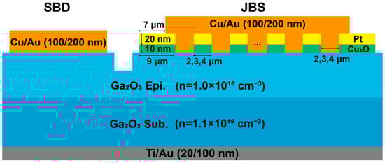
Figure 1.
Cross-sectional schematic image of the β-Ga2O3 SBD and JBS diodes with Cu anode.
The p-type Cu2O film was sputtered by RF magnetron sputtering using a high-purity Cu2O (99.99%) target. The sputtering was carried out at an RF power of 100 W for 3 min. During the deposition, flow rates of 50 sccm Ar and 2 sccm O2 were used to regulate the hole concentration within the Cu2O layers. The resulting p-Cu2O film exhibited a hole concentration of 2.7 × 1019 cm−3 and a mobility of 0.28 cm2/V∙s, as measured by room-temperature Hall effect measurements.
In this study, the hole concentration and mobility of the Cu2O films were characterized using an HL5500PC Hall effect measurement system. The surface morphology and root mean square (RMS) roughness were examined by non-contact 3D surface metrology and device inspection (Sensofar Tech, S.L. (Terrassa, Spain)). The scanning electron microscopy (SEM) image was obtained by EM-40, COXEM. Electrical characterization was carried out using a Keithley 4200-SCS parameter analyzer for room-temperature forward current-voltage (I–V), temperature-dependent I–V, and stress time-dependent I–V measurements, as it provides high-resolution, low-voltage capability suitable for forward characterization. In contrast, the reverse characteristics were measured with an Agilent B1505A system, which can supply the kilovolt-level reverse bias required for high-voltage β-Ga2O3 devices.
3. Results and Discussion
Figure 2 presents the surface morphology and SEM image of the Cu2O/Ga2O3 JBS diode. Figure 2a shows the surface morphology of the Cu2O film, measured using a non-contact 3D surface metrology and device inspection system over a scanning area of 700 μm × 840 μm. The root mean square (RMS) roughness is determined to be 0.18 nm, demonstrating an exceptionally smooth and uniform Cu2O surface. Such low roughness is highly beneficial for device fabrication, as it suppresses interface defect formation at the Cu2O/Ga2O3 heterojunction. Figure 2b displays the SEM image of the fabricated JBS diode, revealing a circular anode pattern with well-defined concentric ring structures. These rings represent the characteristic architecture of the JBS diode design, which facilitates efficient current spreading and a uniform electric field distribution within the active region. The device diameter and fine structural details are distinctly resolved, with a scale bar of 20 μm.
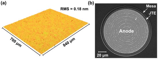
Figure 2.
(a) The non-contact 3D surface profiler image of Cu2O film. (b) The SEM image of the fabricated JBS diode with a spacing of 4 μm.
Figure 3a illustrates the forward I–V characteristics of the fabricated β-Ga2O3 JBS diodes with different Cu2O spacing values (2, 3, and 4 μm), along with a β-Ga2O3 SBD for comparison. The ideality factors of the β-Ga2O3 JBS diodes extracted from the 0.6–1.0 V region are 1.19, 1.32, and 1.21 for spacings of 2, 3, 4 μm, respectively, while the β-Ga2O3 SBD exhibits an ideality factor of 1.16. These values deviate slightly from unity, indicating that Shockley–Read–Hall (SRH) recombination at the heterojunction interface is the dominant transport mechanism under the forward bias, particularly at lower voltages. The relatively higher ideality factor observed in the JBS diode with 3 μm spacing implies enhanced recombination activity, which may arise from localized interface states or inhomogeneous barrier formation [28,29]. As the spacing of the Cu2O region rises, the forward current density correspondingly increases. This behavior can be attributed to the enlarged conduction path in devices with larger spacing, which reduces the influence of the Schottky barrier regions and allows more carriers to flow through the p–n heterojunction. Consequently, the extracted differential specific on-resistance (Ron,sp) of JBS diodes decreases from 6.27 mΩ·cm2 to 6.12 mΩ·cm2 and 5.91 mΩ·cm2 as the spacing increases from 2 to 3 and 4 μm, respectively. The reduction in Ron,sp reflects the improved carrier transport efficiency enabled by the larger effective junction area, which lowers the contribution of series resistance from the depletion region [30]. For comparison, the β-Ga2O3 SBD exhibits a slightly lower Ron,sp of 5.86 mΩ·cm2, highlighting the high-quality interface between the Cu anode and β-Ga2O3.
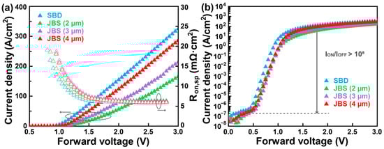
Figure 3.
(a) Linear I–V characteristics and the extracted differential Ron,sp as a function of forward bias for comparison between the β-Ga2O3 JBS diodes and SBD. (b) Semi-logarithmic I–V characteristics for these devices.
Figure 3b depicts the semi-logarithmic I–V characteristics of the β-Ga2O3 JBS diodes and SBD. For a fair comparison, the current density of the SBD and JBS diodes was calculated by normalized the measure current to the full anode area. All diodes exhibit excellent rectifying behavior, with ION/IOFF ratios exceeding 109, confirming the effective suppression of reverse leakage current and the strong rectification capability of the heterojunction structures. The VON, defined at current density of 1 A/cm2, was extracted to be 0.68 V for the SBD and 0.79 V, 0.78 V, and 0.78 V for the JBS diodes with Cu2O spacings of 2, 3, and 4 μm, respectively. The slightly delayed turn-on behavior observed in the JBS diodes compared with the SBD originates from the additional potential barrier introduced by the p–n heterojunctions. This delayed conduction is an intrinsic feature of JBS structures, where the p–n heterojunction regions are designed to block leakage under reverse bias while the Schottky regions dominate forward conduction [31,32].
The reverse I–V characteristics of the diodes are summarized in Figure 4a, with the cathode grounded and the anode reversely biased from 0 V until the reverse current reaches the breakdown criterion of 0.01 A. The SBD shows a BV of 540 V, whereas the JBS diodes achieve significantly higher BV values of 1160 V, 1540 V, and 1700 V for spacings of 2, 3, and 4 μm, respectively. In the JBS diodes, the reverse current shows a relatively weak dependence on the applied reverse bias, primarily due to the depletion-induced pinch-off at the Cu2O/Ga2O3 p–n heterojunctions [33]. Moreover, a wider p-region spacing allows the depletion layer to extend more fully, resulting in a more uniform electric field distribution, alleviating local field crowding, and thereby improving the breakdown characteristics of the device. By contrast, the SBD displays a sudden increase in reverse current at low reverse voltage, which may originate from the impact of interface barrier. These reverse I–V characteristics clearly highlight the superiority of the JBS diodes over the SBD. Figure 4b presents the benchmark plot of the Ron,sp versus BV for the state-of-the-art β-Ga2O3 diodes. The fabricated JBS diode with a 4 μm spacing achieves a PFOM value of 0.49 GW/cm2. This performance is comparable to that of the widely investigated NiO/Ga2O3 JBS diodes, highlighting the strong promise for use in next-generation high-performance power-electronics technology. Table 1 summarized the electrical parameters of all β-Ga2O3 diodes. The SBD exhibits a low Ron,sp of 5.86 mΩ·cm2 and BV of 540 V, corresponding to a PFOM value of 0.05 GW/cm2. In comparison, the JBS diodes with spacings of 2 μm and 3 μm achieve PFOM values of 0.21 GW/cm2 and 0.39 GW/cm2, respectively. Notably, the JBS diode with a 4 μm spacing demonstrates a low Ron,sp of 5.91 mΩ·cm2 and a high BV of 1700 V, further yielding a PFOM value of 0.49 GW/cm2.
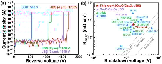
Figure 4.
(a) Reverse I–V characteristics of the β-Ga2O3 JBS diodes with different Cu2O spacing values (2, 3, and 4 μm) and SBD. (b) Benchmark plot of the reported state-of-the-art works on β-Ga2O3 diodes.

Table 1.
Summary of Ron,sp and BV for the β-Ga2O3 diodes.
To further elucidate the influence of Cu2O spacing on the breakdown performance, electric field simulations were conducted on these devices under a reverse voltage of 1000 V. Figure 5 compares the electric field distributions of the β-Ga2O3 SBD and the JBS diodes with Cu2O spacings of 2, 3, and 4 μm, respectively. As shown in Figure 5a, the SBD exhibits pronounced field crowding at the Schottky edge, where the peak electric field reaches 7.34 MV/cm, indicating that the breakdown is dominated by anode edge localization [34]. In contrast, the β-Ga2O3 JBS diodes demonstrate significantly suppressed electric fields of 3.36 MV/cm, 3.19 MV/cm and 3.06 MV/cm for Cu2O spacings of 2, 3, and 4 μm, respectively, accompanied by a smoother and more uniformly distributed field profile along the cutline. The periodic p-type Cu2O regions redistributes the reverse-bias space charge, creating multiple depletion junctions that spread the electric field within the β-Ga2O3 drift layer [35,36]. This effect effectively mitigates edge crowding and yields a more uniform field profile. Consequently, the JBS diodes with Cu2O spacings substantially improves electric field modulation, consistent with the experimentally observed enhancement in breakdown capability.
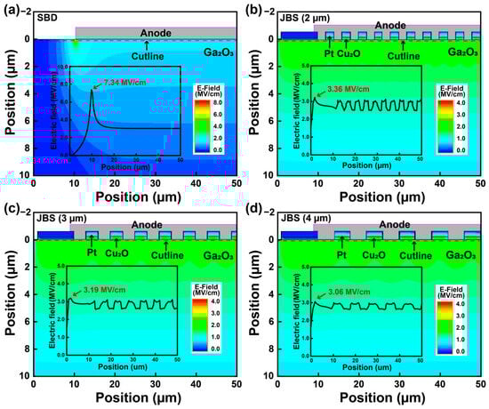
Figure 5.
Electric field distribution of the (a) β-Ga2O3 SBD and (b–d) β-Ga2O3 JBS diodes with different Cu2O spacing values (2, 3, and 4 μm).
Based on the aforementioned electrical characteristics, the JBS diode with a spacing of 4 μm demonstrates superior performance. Therefore, the subsequent evaluations primarily focus on a comparative analysis between the 4 μm JBS diode and the reference SBD. To investigate the thermal stability of these devices, the electrical performance was characterized over the temperature range from 300 K to 425 K. Figure 6 shows the temperature-dependent electrical characteristics of the fabricated β-Ga2O3 JBS diode (4 μm) and SBD. Figure 6a,b present the forward I–V characteristics of the SBD and JBS, respectively. Both devices exhibit typical rectifying behavior, and the VON decreases gradually with increasing temperature, which can be explained by enhanced thermionic emission and the temperature dependence of the Φbi. As temperature rises, the increased carrier energy facilitates barrier crossing, resulting in a lower VON. Figure 6c,d summarize the extracted parameters as a function of temperature. As shown in Figure 6c, the VON decreases from 0.78 V to 0.45 V for the JBS diode and from 0.68 V to 0.43 V for the SBD as the temperature increases. This reduction can be attributed to reduced trap-assisted transport at elevated temperatures, which improves the effective interface quality and reduces barrier inhomogeneity. Figure 6d depicts the temperature dependence of the Ron,sp. With increasing temperature, the Ron,sp increases to 9.97 mΩ·cm2 for the JBS diode and 8.92 mΩ·cm2 for the SBD at 425 K. This increase primarily due to enhanced phonon scattering in the drift layer, which lowers carrier mobility and thereby increases conduction resistance. Notably, the JBS diode consistently exhibits a higher VON and Ron,sp compared to the SBD, which can be attributed to the p–n heterojunctions in the JBS structure. These heterojunctions improve junction uniformity and suppress leakage, but at the cost of increased conduction path resistance [37,38].
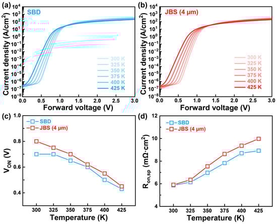
Figure 6.
Temperature-dependent I–V characteristics of β-Ga2O3 (a) SBD and (b) JBS diode. (c,d) are the extracted VON and Ron,sp parameters of the β-Ga2O3 JBS diode and SBD.
Figure 7 illustrates the forward electrical characteristics of the β-Ga2O3 SBD and JBS (4 μm) diodes under different stress time at room temperature. Figure 7a illustrates the measurement–stress–measurement scheme used to evaluate the long-term reliability of the SBD and JBS devices. Figure 7b,c present the forward I–V curves after stress times ranging from 0.01 s to 5000 s under reverse stress of 200 V, a level selected to prevent premature breakdown during extended stress testing. Both devices exhibit a gradual increase in forward current with prolonged stress time, which can be ascribed to stress-induced barrier modification and the generation of interface state. These defect states locally reduce the effective Φbi, thereby enhancing carrier transport [39,40]. The degradation effect is more evident in the SBD, whereas the JBS diode exhibits improved stability because the p–n heterojunctions effectively suppress barrier fluctuations and limit the influence of localized interface degradation [41,42]. Figure 7d,e summarize the extracted electrical parameters as a function of stress time. As shown in Figure 7d, the VON of the SBD increases significantly with prolonged stress time, deteriorating by 17.45%. This behavior arises from charge trapping and barrier inhomogeneity, which hinder uniform current conduction [43]. In contrast, the JBS diode shows only a 4.16% deterioration in VON, indicating that the p–n heterojunctions stabilize the barrier profile and ensure more uniform potential distribution [44]. Similarly, the dynamic specific on-resistance variation (∆Ron,sp) increases with stress time for both devices due to enhanced phonon scattering and the accumulation of trapped charges. However, the JBS diode consistently maintains a lower ∆Ron,sp, increasing only to 1.15 after 5000 s, compared to 1.24 for the SBD. This reduced degradation highlights the capability of the JBS diode to alleviate current crowding and suppress defect-assisted conduction pathways [45]. Overall, these results confirm that the JBS structure offers enhanced reliability and stronger resistance to stress-induced performance degradation compared with the conventional SBD.
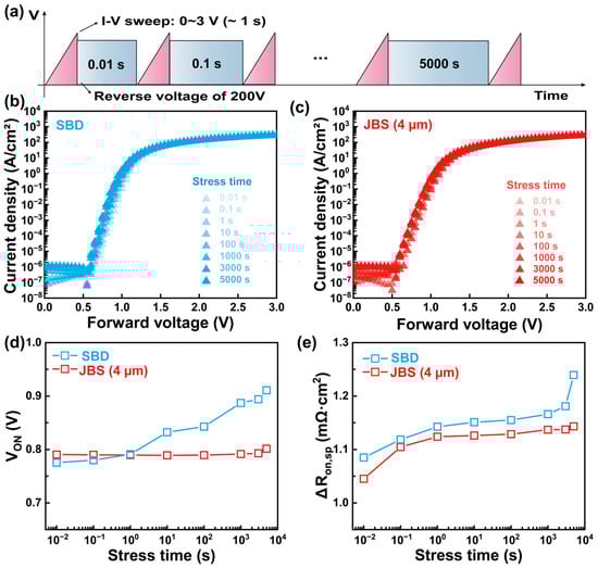
Figure 7.
(a) Measurement-stress-measurement scheme for long-term reliability test. Linear-scale forward I–V characteristics of the β-Ga2O3 (b) SBD and (c) JBS diode after various stress times. (d,e) are the extracted corresponding VON and ∆Ron,sp as a function of the stress time, respectively.
4. Conclusions
In summary, the Cu2O/Ga2O3 JBS diode achieves a favorable balance between low conduction loss and high BV, benefiting from the combined roles of the Cu anode and the p–n heterojunctions. The JBS diode with a 4 μm spacing features a low VON of 0.78 V, a high BV of 1700 V and a Ron,sp of 5.91 mΩ·cm2, yielding a PFOM of 0.49 GW/cm2. Moreover, it also exhibits excellent thermal stability and superior resistance to stress-induced degradation, with only a 4.16% increase in VON and a modest 1.15-fold rise in ∆Ron,sp under a 200 V reverse stress for 5000 s. These findings validate the effectiveness of the Cu2O/Ga2O3 JBS structure as a robust strategy for advancing β-Ga2O3-based power electronics, paving the way toward the next generation of high-efficiency and high-voltage devices.
Author Contributions
Conceptualization, X.W.; methodology, X.W., X.L., M.L. and H.Y. (Haozhe Yu); formal analysis, X.W., K.W.A. and C.Z.C.; investigation, X.W., M.L. and Y.G.; writing—original draft preparation, X.W.; writing—review and editing, Q.W. and H.Y. (Hongyu Yu); funding acquisition, H.Y. (Hongyu Yu). All authors have read and agreed to the published version of the manuscript.
Funding
This work was supported by the National Natural Science Foundation of China (Grant No: 62274082), Research on mechanism of Source/Drain ohmic contact and the related GaN p-FET (Grant No: 2023A1515030034), Study on the reliability of GaN power devices (Grant No: JCYJ20220818100605012), Research on novelty low-resistance Source/Drain ohmic contact for GaN p-FET (Grant No: JCYJ20220530115411025), and Research on GaN-Based Devices for Industrial Applications (Grant No. 6025312001K).
Data Availability Statement
The data that support the findings of this study are available from the corresponding authors upon reasonable request.
Acknowledgments
The authors acknowledge the assistance of SUSTech Core Research Facilities.
Conflicts of Interest
The authors declare no conflicts of interest.
References
- Zhang, Y.H.; Udrea, F.; Wang, H. Multidimensional device architectures for efficient power electronics. Nat. Electron. 2022, 5, 723–734. [Google Scholar] [CrossRef]
- Zhou, F.; Gong, H.H.; Xiao, M.; Ma, Y.W.; Wang, Z.P.; Yu, X.X.; Li, L.; Fu, L.; Tan, H.H.; Yang, Y.; et al. An avalanche-and-surge robust ultrawide-bandgap heterojunction for power electronics. Nat. Commun. 2023, 14, 4459. [Google Scholar]
- Pearton, S.J.; Yang, J.C.; Cary, P.H.; Ren, F.; Kim, J.; Tadjer, M.J.; Mastro, M.A. A review of Ga2O3 materials, processing, and devices. Appl. Phys. Rev. 2018, 5, 011301. [Google Scholar] [CrossRef]
- Sun, S.H.; Wang, C.L.; Alghamdi, S.; Zhou, H.; Hao, Y.; Zhang, J.C. Recent advanced ultra-wide bandgap β-Ga2O3 material and device technologies. Adv. Electron. Mater. 2024, 11, 2300844. [Google Scholar] [CrossRef]
- Tsao, J.Y.; Chowdhury, S.; Hollis, M.A.; Jena, D.; Johnson, N.M.; Jones, K.A.; Kaplar, R.J.; Rajan, S.; Van de Walle, C.G.; Bellotti, E.; et al. Ultrawide-Bandgap Semiconductors: Research Opportunities and Challenges. Adv. Electron. Mater. 2018, 4, 1600501. [Google Scholar] [CrossRef]
- Wang, C.L.; Zhang, J.C.; Xu, S.R.; Zhang, C.F.; Feng, Q.; Zhang, Y.C.; Ning, J.; Zhao, S.L.; Zhou, H.; Hao, Y. Progress in state-of-the-art technologies of Ga2O3 devices. J. Phys. D-Appl. Phys. 2021, 54, 243001. [Google Scholar] [CrossRef]
- He, Q.M.; Hao, W.B.; Zhou, X.Z.; Li, Y.; Zhou, K.; Chen, C.; Xiong, W.H.; Jian, G.Z.; Xu, G.W.; Zhao, X.L.; et al. Over 1 GW/cm2 vertical Ga2O3 Schottky barrier diodes without edge termination. IEEE Electron Device Lett. 2022, 43, 264–267. [Google Scholar] [CrossRef]
- Li, J.S.; Chiang, C.C.; Xia, X.; Yoo, T.J.; Ren, F.; Kim, H.; Pearton, S.J. Demonstration of 4.7 kV breakdown voltage in NiO/β-Ga2O3 vertical rectifiers. Appl. Phys. Lett. 2022, 121, 042105. [Google Scholar] [CrossRef]
- Lu, X.; Zhou, X.D.; Jiang, H.X.; Ng, K.W.; Chen, Z.M.; Pei, Y.L.; Lau, K.M.; Wang, G. 1-kV sputtered p-NiO/n-Ga2O3 heterojunction diodes with an ultra-low leakage current below 1 μA/cm2. IEEE Electron Device Lett. 2020, 41, 449–452. [Google Scholar] [CrossRef]
- Qin, Y.; Xiao, M.; Porter, M.; Ma, Y.W.; Spencer, J.; Du, Z.H.; Jacobs, A.G.; Sasaki, K.; Wang, H.; Tadjer, M.; et al. 10-kV Ga2O3 charge-balance Schottky rectifier perational at 200 °C. IEEE Electron Device Lett. 2023, 44, 1268–1271. [Google Scholar] [CrossRef]
- Titov, A.I.; Karabeshkin, K.V.; Struchkov, A.I.; Nikolaev, V.I.; Azarov, A.; Gogova, D.S.; Karaseov, P.A. Comparative study of radiation tolerance of GaN and Ga2O3 polymorphs. Vacuum 2022, 200, 111005. [Google Scholar] [CrossRef]
- Hoshikawa, K.; Kobayashi, T.; Ohba, E. 50 mm diameter Sn-doped (001) β-Ga2O3 crystal growth using the vertical Bridgeman technique in ambient air. J. Cryst. Growth 2020, 546, 125778. [Google Scholar] [CrossRef]
- Reese, S.B.; Remo, T.; Green, J.; Zakutayev, A. How Much Will Gallium Oxide Power Electronics Cost? Joule 2019, 3, 903–907. [Google Scholar] [CrossRef]
- Tomm, Y.; Reiche, P.; Klimm, D.; Fukuda, T. Czochralski grown Ga2O3 crystals. J. Cryst. Growth 2000, 220, 510–514. [Google Scholar] [CrossRef]
- Víllora, E.G.; Shimamura, K.; Yoshikawa, Y.; Aoki, K.; Ichinose, N. Large-size β-Ga2O3 single crystals and wafers. J. Cryst. Growth 2004, 270, 420–426. [Google Scholar] [CrossRef]
- Almaev, A.; Nikolaev, V.; Yakovlev, N.; Butenko, P.; Tsymbalov, A.; Boiko, M.; Kopyev, V.; Krymov, V.; Kushnarev, B.; Shapenkov, S.; et al. Electroconductive and photoelectric properties of Pt/(100) β-Ga2O3 Schottky barrier diode based on Czochralski grown crystal. J. Vac. Sci. Technol. A 2024, 42, 042802. [Google Scholar] [CrossRef]
- Li, W.S.; Saraswat, D.; Long, Y.Y.; Nomoto, K.; Jena, D.; Xing, H.G. Near-ideal reverse leakage current and practical maximum electric field in β-Ga2O3 Schottky barrier diodes. Appl. Phys. Lett. 2020, 116, 192101. [Google Scholar] [CrossRef]
- Yakovlev, N.N.; Almaev, A.V.; Kushnarev, B.O.; Verkholetov, M.G.; Poliakov, M.V.; Zinovev, M.M. β-Ga2O3 Schottky Barrier Diode with Ion Beam Sputter-Deposited Semi-Insulating Layer. Crystals 2024, 14, 123. [Google Scholar] [CrossRef]
- Takatsuka, A.; Miyamoto, H.; Sasaki, K.; Kuramata, A. Fabrication of ampere-class p-Cu2O/n-β-Ga2O3 trench heterojunction barrier Schottky diodes and double-pulse evaluation. In Proceedings of the 35th International Symposium on Power Semiconductor Devices and ICs (ISPSD), Hong Kong, China, 28 May–1 June 2023; pp. 342–345. [Google Scholar] [CrossRef]
- Wei, J.; Wei, Y.X.; Lu, J.; Peng, X.S.; Jiang, Z.L.; Yang, K.M.; Luo, X.R. Experimental Study on Electrical Characteristics of Large-Size Vertical β-Ga2O3 Junction Barrier Schottky Diodes. In Proceedings of the 34th IEEE International Symposium on Power Semiconductor Devices and ICs (ISPSD), Vancouver, BC, Canada, 22–25 May 2022; pp. 97–100. [Google Scholar] [CrossRef]
- Gong, H.H.; Yu, X.X.; Xu, Y.; Chen, X.H.; Kuang, Y.; Lv, Y.J.; Yang, Y.; Ren, F.F.; Feng, Z.H.; Gu, S.L.; et al. β-Ga2O3 vertical heterojunction barrier Schottky diodes terminated with p-NiO field limiting rings. Appl. Phys. Lett. 2021, 118, 202102. [Google Scholar] [CrossRef]
- He, Q.M.; Hao, W.B.; Li, Q.Y.; Han, Z.; He, S.; Liu, Q.; Zhou, X.Z.; Xu, G.W.; Long, S.B. β-Ga2O3 junction barrier Schottky diode with NiO p-well floating field rings. Chin. Phys. B 2023, 32, 128507. [Google Scholar] [CrossRef]
- Lv, Y.J.; Wang, Y.G.; Fu, X.C.; Dun, S.B.; Sun, Z.F.; Liu, H.Y.; Zhou, X.Y.; Song, X.B.; Dang, K.; Liang, S.X.; et al. Demonstration of β-Ga2O3 Junction Barrier Schottky Diodes with a Baligas Figure of Merit of 0.85 GW/cm2 or a 5A/700 V Handling Capabilities. IEEE Trans. Power Electron. 2021, 36, 6179–6182. [Google Scholar] [CrossRef]
- Wu, F.H.; Wang, Y.A.; Jian, G.Z.; Xu, G.W.; Zhou, X.Z.; Guo, W.; Du, J.H.; Liu, Q.; Dun, S.; Yu, Z.A.; et al. Superior Performance β-Ga2O3 Junction Barrier Schottky Diodes Implementing p-NiO Heterojunction and Beveled Field Plate for Hybrid Cockcroft-Walton Voltage Multiplier. IEEE Trans. Electron Devices 2023, 70, 1199–1205. [Google Scholar] [CrossRef]
- Wang, J.J.; Ji, X.Q.; Zheng, H.C.; Ye, L.C.; Liu, Z.; Shu, L.; Li, S.; Tang, W.H.; Li, P.G. Investigation of electrical transport mechanisms in p-NiO/n-Ga2O3 junction barrier Schottky diodes with low leakage and high breakdown voltage. Phys. Scr. 2025, 100, 105904. [Google Scholar] [CrossRef]
- Su, C.X.; Zhou, H.; Zhang, K.; Wang, C.L.; Sun, S.H.; Gong, H.H.; Ye, J.D.; Liu, Z.H.; Dang, K.; Hu, Z.Y.; et al. Low turn-on voltage and 2.3 kV β-Ga2O3 heterojunction barrier Schottky diodes with Mo anode. Appl. Phys. Lett. 2024, 124, 173506. [Google Scholar] [CrossRef]
- Gong, H.H.; Sun, N.; Hu, T.C.; Porter, M.; Yu, X.X.; Ren, F.F.; Gu, S.L.; Zheng, Y.D.; Zhang, R.; Zhang, Y.H.; et al. Kilovolt, low-barrier Ga2O3 JBS diode with ultra-low forward voltage. In Proceedings of the 36th International Symposium on Power Semiconductor Devices and ICs (ISPSD), Bremen, Germany, 2–6 June 2024; pp. 104–107. [Google Scholar] [CrossRef]
- Li, M.J.; He, M.H.; Wang, X.H.; Jiang, Y.; Wen, K.Y.; Du, F.Z.; Deng, C.K.; He, J.Q.; Zhang, Y.; Yu, W.Y.; et al. High-performance β-Ga2O3 Schottky barrier diodes with Mg current blocking layer using spin-on-glass technique. Appl. Phys. Lett. 2024, 125, 132101. [Google Scholar] [CrossRef]
- Tung, R.T. Recent advances in Schottky barrier concepts. In Materials Science & Engineering R-Reports; Elsevier: Amsterdam, The Netherlands, 2001; Volume 35, pp. 1–138. [Google Scholar] [CrossRef]
- Wang, X.H.; Li, M.J.; He, M.H.; Lu, H.H.; Chen, C.Z.; Jiang, Y.; Wen, K.Y.; Du, F.Z.; Zhang, Y.; Deng, C.K.; et al. Optimization of CuOx/Ga2O3 Heterojunction Diodes for High-Voltage Power Electronics. Nanomaterials 2025, 15, 87. [Google Scholar] [CrossRef]
- Wang, X.H.; Li, M.J.; Jiang, Y.; Wen, K.Y.; Tang, C.Y.; Du, F.Z.; Chen, C.Z.; Deng, C.K.; Zhang, Y.; Lu, H.H.; et al. 2.86-kV vertical Cu2O/Ga2O3 heterojunction diodes with stepped double-layer structure. J. Alloys Compd. 2025, 1036, 181672. [Google Scholar] [CrossRef]
- Wang, Y.G.; Gong, H.H.; Lv, Y.J.; Fu, X.C.; Dun, S.B.; Han, T.T.; Liu, H.Y.; Zhou, X.Y.; Liang, S.X.; Ye, J.D.; et al. 2.41 kV vertical P-Nio/n-Ga2O3 heterojunction diodes with a record Baliga’s Figure-of-Merit of 5.18 GWcm2. IEEE Trans. Power Electron. 2022, 37, 3743–3746. [Google Scholar] [CrossRef]
- Watahiki, T.; Yuda, Y.; Furukawa, A.; Yamamuka, M.; Takiguchi, Y.; Miyajima, S. Heterojunction p-Cu2O/n-Ga2O3 diode with high breakdown voltage. Appl. Phys. Lett. 2017, 111, 222104. [Google Scholar] [CrossRef]
- Wang, C.L.; Yan, Q.L.; Zhang, C.Q.; Su, C.X.; Zhang, K.; Sun, S.H.; Liu, Z.H.; Zhang, W.H.; Alghamdi, S.; Ghandourah, E.; et al. β-Ga2O3 lateral Schottky barrier diodes with >10 kV breakdown voltage and anode engineering. IEEE Electron Device Lett. 2023, 44, 1684–1687. [Google Scholar] [CrossRef]
- Kong, L.X.; Ren, N.; Wang, R.; Li, Y.J.; Wang, C.; Wang, H.Y.; Sheng, K. Fabrication and Characterization of Kilovolt p-Type SiC JBS Diodes with Enhanced Current Capability and Electroluminescence Phenomenon. IEEE Electron Device Lett. 2024, 45, 1566–1569. [Google Scholar] [CrossRef]
- Zhou, H.; Zeng, S.F.; Zhang, J.C.; Liu, Z.H.; Feng, Q.; Xu, S.R.; Zhang, J.F.; Hao, Y. Comprehensive Study and Optimization of Implementing p-NiO in β-Ga2O3 Based Diodes via TCAD Simulation. Crystals 2021, 11, 1186. [Google Scholar] [CrossRef]
- Gong, H.H.; Sun, N.; Hu, T.C.; Yu, X.X.; Porter, M.; Yang, Z.E.; Ren, F.F.; Gu, S.L.; Zheng, Y.D.; Zhang, R.; et al. Ga2O3/NiO junction barrier Schottky diodes with ultra-low barrier TiN contact. Appl. Phys. Lett. 2024, 124, 233507. [Google Scholar] [CrossRef]
- Wilhelmi, F.; Kunori, S.; Sasaki, K.; Kuramata, A.; Komatsu, Y.; Lindemann, A. Packaged β-Ga2O3 Trench MOS Schottky Diode with Nearly Ideal Junction Properties. IEEE Trans. Power Electron. 2022, 37, 3737–3742. [Google Scholar] [CrossRef]
- Sze, S.M. Physics of Semiconductor-Devices, 3rd ed.; Wiley-Interscience: Hoboken, NJ, USA, 2007. [Google Scholar] [CrossRef]
- Tung, R.T. Electron transport at metal-semiconductor interfaces: General theory. Phys. Rev. B 1992, 45, 13509–13523. [Google Scholar] [CrossRef]
- Jiang, Z.L.; Wei, J.; Lv, Y.J.; Wei, Y.X.; Wang, Y.G.; Lu, J.; Liu, H.Y.; Feng, Z.H.; Zhou, H.; Zhang, J.C.; et al. Nonuniform mechanism for positive and negative bias stress instability in β-Ga2O3 MOSFET. IEEE Trans. Electron Devices 2022, 69, 5509–5515. [Google Scholar] [CrossRef]
- Wang, H.; Lai, C.H.; Huang, P.Y.; Lin, Y.A.; Hsu, S.S.H.; Wong, R.K.Y. Comprehensive Study on Trapping-induced Dynamics in β-Ga2O3 Schottky Barrier Diodes under Continuous Switching Stress. In Proceedings of the 36th International Symposium on Power Semiconductor Devices and ICs (ISPSD), Bremen, Germany, 2–6 June 2024; pp. 224–227. [Google Scholar] [CrossRef]
- Zhang, T.; Lv, Y.G.; Li, R.H.; Zhang, Y.N.; Zhang, Y.C.; Li, X.D.; Zhang, J.C.; Hao, Y. Current-collapse suppression of high-performance lateral AlGaN/GaN Schottky barrier diodes by a thick GaN cap layer. IEEE Electron Device Lett. 2021, 42, 477–480. [Google Scholar] [CrossRef]
- Callahan, W.A.; Egbo, K.; Lee, C.W.; Ginley, D.; O’Hayre, R.; Zakutayev, A. Reliable operation of Cr2O3:Mg/β-Ga2O3 p-n heterojunction diodes at 600 °C. Appl. Phys. Lett. 2024, 124, 153504. [Google Scholar] [CrossRef]
- Gong, H.H.; Yang, X.; Porter, M.; Yang, Z.N.; Wang, B.X.; Li, L.; Fu, L.; Sasaki, K.; Wang, H.; Gu, S.L.; et al. Reliability of NiO/β-Ga2O3 bipolar heterojunction. Appl. Phys. Lett. 2025, 126, 012102. [Google Scholar] [CrossRef]
Disclaimer/Publisher’s Note: The statements, opinions and data contained in all publications are solely those of the individual author(s) and contributor(s) and not of MDPI and/or the editor(s). MDPI and/or the editor(s) disclaim responsibility for any injury to people or property resulting from any ideas, methods, instructions or products referred to in the content. |
© 2025 by the authors. Licensee MDPI, Basel, Switzerland. This article is an open access article distributed under the terms and conditions of the Creative Commons Attribution (CC BY) license (https://creativecommons.org/licenses/by/4.0/).