Article

Tunable Electronic Bandgaps and Optical and Magnetic Properties in Antiferromagnetic MPS3/GaN (M = Mn, Fe, and Ni) Heterobilayers

1
The College of Physics, Donghua University, Shanghai 201620, China
2
College of Physics and Optoelectronic Engineering, Hangzhou Institute for Advanced Study, University of Chinese Academy of Sciences, No. 1, Sub-Lane Xiangshan, Xihu District, Hangzhou 310024, China
3
College of Optical and Electronic Technology, China Jiliang University, Hangzhou 310018, China
4
State Key Laboratory of Infrared Physics, Shanghai Institute of Technical Physics, Chinese Academy of Sciences, Shanghai 200083, China
*
Authors to whom correspondence should be addressed.
Nanomaterials 2025, 15(11), 832; https://doi.org/10.3390/nano15110832
Submission received: 21 April 2025 / Revised: 23 May 2025 / Accepted: 28 May 2025 / Published: 30 May 2025

Abstract

Research on two dimensional (2D) antiferromagnetic materials and heterobilayers is gaining prominence in spintronics. This study focuses on MPS3 monolayers and their van der Waals heterobilayers with GaN monolayers. We systematically investigated the structural stability, electronic properties, and magnetic characteristics of MPS3 (M = Mn, Fe, and Ni) monolayers via first-principles calculations, and explored their potential applications in optoelectronics and spintronics. Through phonon spectrum analysis, the dynamic stability of MPS3 monolayers was confirmed, and their bond lengths, charge distributions, and wide-bandgap semiconductor properties were analyzed in detail. In addition, the potential applications of MPS3 monolayers in UV detection were explored. Upon constructing the MPS3/GaN heterobilayer structure, a significant reduction in the bandgap was observed, thereby expanding its potential applications in the visible light spectrum. The intrinsic antiferromagnetic nature of MPS3 monolayers was confirmed through calculations, with the magnetic moments of the magnetic atoms M being 4.560, 3.672, and 1.517, respectively. Moreover, the heterobilayer structures further enhanced the magnetic moments of these elements. The magnetic properties of MPS3 monolayers were further analyzed using spin-orbit coupling (SOC), confirming their magnetic anisotropy. These results provide a theoretical basis for the design of novel two-dimensional spintronic and optoelectronic devices based on MPS3.

1. Introduction

In 2004, Novoselov and Geim investigated graphene’s monolayer structure, confirming the possibility of exfoliating stable single-atom or single-polyhedron thickness two dimensional (2D) materials from van der Waals solids [1,2,3]. Since then, there has been sustained enthusiasm for exploring layered van der Waals materials, with their unique and fascinating physical properties gaining attention. Many materials that can be exfoliated and studied in the 2D limit have been discovered or rediscovered [4,5]. Building on this, the discovery of magnetic ordering phenomena in 2D van der Waals materials at the 2D limit has made it possible to systematically study the effects of dimensionality on magnetic ordering and to integrate magnetic materials into van der Waals heterostructures [6,7,8,9]. Long-range magnetic order has been observed in materials such as Cr2Ge2Te6, Fe3GeTe2, and CrI3. Moreover, many inherently non-magnetic two-dimensional materials, such as graphene, hexagonal BN, and transition metal dichalcogenides, can exhibit magnetic properties through defect engineering, strain manipulation, and chemical modifications. This avenue of research holds promise for expanding the scope of magnetic functionalities in 2DM and advancing spintronic applications. Recently, scientists have focused their attention on exploring and utilizing many different magnetic states, including ferromagnetic (FM) and antiferromagnetic (AFM) ground states, while controlling magnetism through external stimuli such as strain engineering, defects, and electric fields, and modifying the arrangement of the magnetocrystalline arrays, leading to the discovery of compelling physical phenomena. Interestingly, although AFM states are internally magnetic, their net magnetization is zero, which may lead to a variety of remarkable phenomena in 2D confinement [10]. Furthermore, combining electrical, optical, and magnetic properties can lead to mesmerizing magnetoelectric or magneto-optical coupling effects [11,12].
Intralayer AFM materials encompass a diverse array of compounds that have garnered increasing interest. Leading the pack in this category are transition metal thiophosphates MPS3 (M = Mn, Fe, Co, or Ni) and selenophosphates MPSe3 (M = Mn, Fe, or Ni), where layered AFM has been meticulously examined and confirmed through various experimental methodologies. FePS3, CoPS3, NiPS3, and FePSe3 exhibit a zigzag-type AFM arrangement, while MnPS3 and MnPSe3 demonstrate Néel-type ordering [13,14,15,16]. Further intricacies emerge in the cases of FePS3, FePSe3, and MnPS3, which feature out-of-plane anisotropy, contrasting with the dominant in-plane anisotropy observed in NiPS3 and MnPSe3. Previous investigations have revealed that the bulk form of these materials with M = Mn, Fe, and Ni exhibit AFM behavior, with Neel temperatures measured at 78 K, 123 K, and 155 K, respectively [17]. Additionally, studies have delved into the metal-to-insulator transition and the emergence of superconducting phases within this family of compound [18,19,20]. These unique properties make MPS3 family materials promising candidates for a wide range of applications in the fields of electronics, spintronics, and quantum technologies. Further research into their fundamental properties and potential technological applications is warranted to fully harness their capabilities. Recent reports have demonstrated an all-optical control of the magnetic anisotropy in NiPS3 by tuning the photon energy in resonance with an orbital transition between crystal field-split levels. This finding opens up a new application direction for utilizing the potential of transition metal phosphorus trichalcogenides in the field of optical control, paving the way for new possibilities in areas such as optoelectronics and information storage technologies.
Understanding and controlling surfaces is crucial for designing and developing new materials with specific properties and functionalities. The integration of two or more types of 2D van der Waals heterobilayers (vdWHs) along the vertical direction introduces novel properties [21,22,23,24,25,26,27,28,29,30,31]. In this work, considering all the superior properties of both MPS3 (M = Mn, Fe, and Ni) and GaN nanosheets, we constructed the MPS3/GaN vdWHs (in the following text, the MPS3/GaN vdWHs will be uniformly abbreviated as vdWHs) and investigate their electronic, magnetic, and optical properties using DFT. The work is organized as follows: a brief overview of computational information is provided in Section 2; detailed electronic, magnetic, and optical properties for MPS3 MLs and vdWHs are discussed in Section 3. Finally, a summary is provided in Section 4.

2. Computational Information

All DFT calculations were performed by using the projector-augmented wave (PAW) [32] pseudopotential, as implemented in the Vienna ab initio Simulation Package (VASP) [33,34]. For structural optimizations and energy calculations, the exchange-correlation potential based on the Perdew–Burke–Ernzerhof function with a generalized gradient approximation (PBE-GGA) was used [35,36]. To make sure all geometric structures were fully relaxed, the energy and force convergence on each atom were set to 10−5 eV/atom and 0.001 eV/Å, respectively. The Monkhorst–Pack method with 5 × 5 × 1 K-points meshes of Brillouin zones was selected for geometric relaxation and 15 × 15 × 1 k-mesh was used for calculating the density of states (DOS). Moreover, the Hubbard-like Coulomb interaction U and the Screened Stoner exchange parameter J are considered. The effective parameter is defined as Ueff = U − J and applied on the M (Mn, Fe, and Ni) 3d orbitals, and has been set to 4.0, 4.6, and 5.1 eV, respectively. These values have been studied before [37]. The DFT-D3 method was adopted to address the issue of inaccurate dispersion description by PBE [38]

3. Results and Discussion

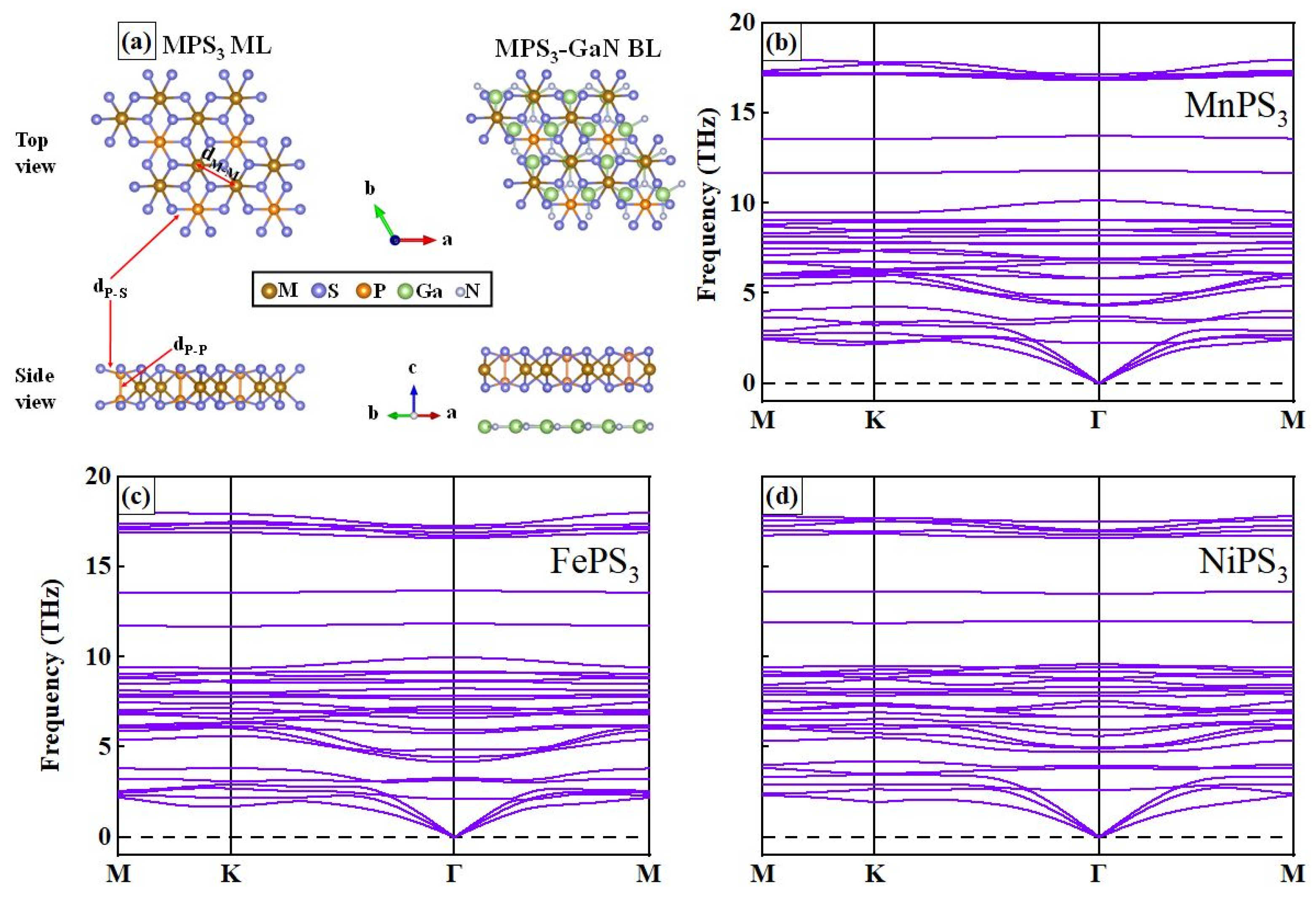
3.1. Structural Properties and Stability

The top and side views of the atomic structures of free-standing GaN MLs was relaxed to a flat honeycomb structure which was stripped from the (0001) plane of a wurtzite GaN structure (which has been analyzed before) [39]. MPS3 belongs to layered vdWs materials, as shown in Figure 1a, and M atoms are sandwiched by P- and S-constituted planes. We first calculated the energy difference of the system (△E = EAFM − EFM) and presented the results in Table 1 and Table S2. The negative values for both MPS3 MLs and vdWHs indicate that the ground state of the three MPS3 MLs is AFM. The persistence of the AFM state in the vdWHs also indicates that the interfacial interactions do not significantly disrupt the magnetic ordering, which is an important consideration for designing layered materials with tailored properties.
As shown in Table 1, the calculated lattice parameters of GaN, MnPS3, FePS3, NiPS3 MLs are a = b = 6.38 Å, 6.13 Å, 6.00 (a ≈ b) Å, and 5.89 Å, respectively (as shown in Table 1). The lattice mismatch between MPS3 and GaN MLs were calculated to 4.07%, 6.33%, and 8.32%, respectively. Based on these data, it can be observed that the lattice mismatches of MnPS3, FePS3, and NiPS3 MLs are all below 10%. This indicates that the lattice mismatches are relatively small, making them suitable for constructing vdWHs. A smaller lattice mismatch promotes a tighter interface between the two materials, which is beneficial for optimizing electronic transport and optical properties. Therefore, these materials can be widely applied in the design and fabrication of vdWHs to achieve enhanced performance and application potential.
The stability of the structure of MPS3 MLs was explored through various methods initially. Phonon dispersion calculations were conducted to verify dynamic stability. As depicted in Figure 1b–d, no imaginary frequency modes were observed within the Brillouin zone for all 2D MPS3 MLs, confirming their dynamic stability. The absence of imaginary frequencies indicates that these materials do not exhibit any unstable vibrational modes that could lead to structural deformations or instabilities. This finding is essential as it assures the reliability and long-term viability of MPS3 MLs in practical applications. The computed bond length between M and M atoms (dM-M), the bond length between M and P atoms (dM-P), and the distance between P and X atoms (dP-S) for relaxed MPS3 MLs are shown in Table 1. In the MPS3 (M = Mn, Fe, and Ni) MLs, it is evident that the values of dM-M decrease sequentially as 3.54 Å, 3.42 Å, and 3.39 Å. Additionally, the differences of dP-S and dP-P are about 2.00 Å and 2.04 Å (the differences between these three structures can be considered negligible). In the MPS3 MLs, a systematic reduction in the interatomic distance between M atoms was observed and this trend may be influenced by the varying electronegativities of these transition metal elements, affecting the strengths of their bonding interactions.
In pure GaN ML, the Ga−N bond length is 1.842 Å, while in vdWHs, it shortens to 1.822 Å, 1.813 Å, and 1.805 Å (shown in Table S1). The bond length reductions indicate strengthened Ga−N bonds in vdWHs, implying increased bond energy and enhanced bond stability. By examining Table 1, it is evident that under the influence of GaN ML, vdWHs experience lattice expansion. The lattice constants (a values) of these three vdWHs are found to be 6.42 Å, 6.39 Å, and 6.22 Å, respectively. This expansion leads to an increased distance between M atoms within the vdWHs. The observed lattice expansion can be attributed to the interlayer interactions between the GaN and MPS3 MLs. These interactions alter the equilibrium positions of the atoms, resulting in larger lattice constants and expanded unit cell sizes. The increased distance between M atoms implies a weakening of their interatomic interactions. Changes in interatomic spacing have significant implications for the electronic and structural properties of vdWHs, impacting their optical, electrical, and magnetic characteristics. It is worth noting that these changes extend beyond mere lattice expansion. Further investigation is warranted to fully comprehend the overall impact on the behavior and performance of vdWHs.
Binding energy (Eb) represents the difference in the total energy of the vdWHs and their parent MLs as follows: Eb = Etotal − EMPS3 − EGaN. Where Etotal, EMPS3, and EGaN correspond to the energies of MPS3/GaN vdWHs, MPS3 and GaN MLs, respectively [40]. A positive Eb value indicates an endothermic reaction, where the energy of the system increases from reactants to products. Conversely, a negative Eb signifies an exothermic reaction, where energy is released as the system transitions from reactants to products. Our calculations reveal that the Eb of the vdWHs are −0.566 eV, −0.571 eV, and −0.591 eV, respectively (as shown in Table 1). The fact that all three vdWHs exhibit negative Eb values, which are also numerically similar, suggests that they possess similar binding strengths. The negative Eb indicates that energy is released during the formation of the vdWHs, implying that these BLs are thermodynamically stable. This stability is a crucial characteristic for the practical applications of vdWHs in fields such as optoelectronic devices, sensors, and catalysts. Moreover, the similar Eb values may imply structural and electronic property similarities among these vdWHs, which could be instructive for their performance in analogous applications.

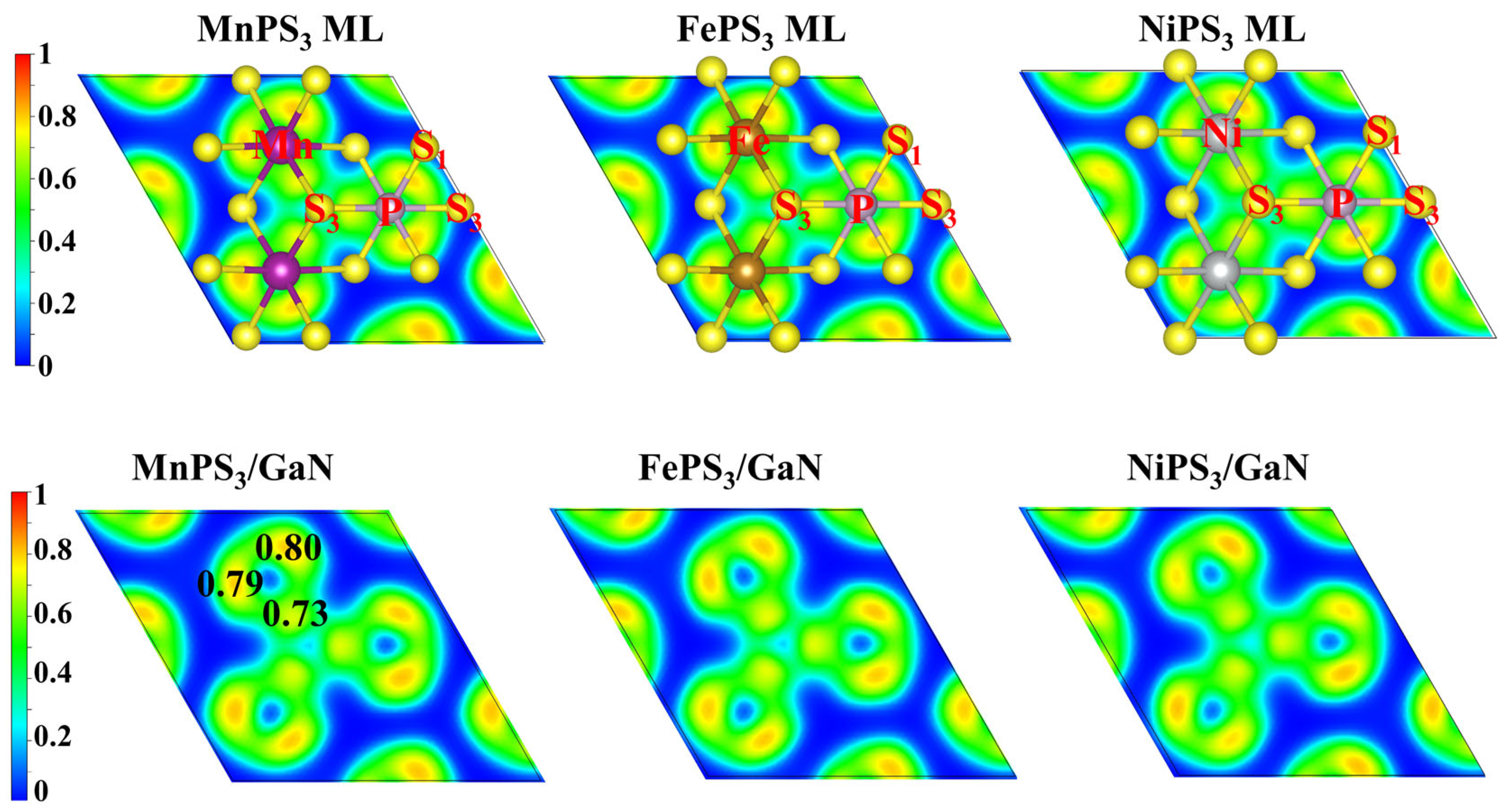
3.2. Charge Analysis

As shown in Figure 2, the Electron Localization Function (ELF) is commonly used to determine the bonding characteristics and the degree of electron localization, with its value ranging between 0 and 1. Here, ELF = 0 corresponds to the absence of electron distribution, while ELF = 0.5 represents a homogeneous electron gas. In contrast, ELF = 1 indicates complete electron localization at a specific site. Through computational analysis, it is found that both Mn and P atoms form bonds with S atoms, with ELF values ranging between 0.73 and 0.80. This suggests a strong covalent bonding interaction between these atoms, as ELF values closer to 1 signify higher electron localization and stronger covalent character. The ELF distribution around the bonding regions reveals a significant overlap of electron density between Mn–S and P–S, indicating the formation of stable chemical bonds. The relatively high ELF values (0.73~0.80) further support the conclusion that the electrons are highly localized in these bonding regions, which is characteristic of covalent interactions. Moreover, in the construction of the heterostructure bilayer, the ELF values remain consistently within this range (0.73–0.80). This indicates that the covalent bonding characteristics and electron localization behavior between Mn, P, and S atoms are preserved even in the heterostructure configuration. This analysis provides valuable insights into the electronic structure and bonding nature of the system, highlighting the importance of ELF in understanding the chemical properties and stability of the material.
To further analyze the electron distribution within the system, we employed the Bader charge analysis method. Bader analysis is a quantitative method based on the topological structure of the electron density. It can accurately partition the charge distribution between atoms and calculate the net charge carried by each atom. Through Bader analysis, we calculated the net charges of Mn, P, S, Ga, and N atoms and observed a distinct charge transfer phenomenon. As shown in Table 1, in the MPS3 MLs, M atoms and P atoms lose electrons, while S atoms gain electrons. This indicates that electrons are transferred from M atoms and P atoms to S atoms. This further confirms the polar characteristics of the M–S and P–S bonds, and this charge transfer behavior is consistent with the covalent bond characteristics observed in the ELF analysis. As the number of outermost electrons (M-d) increases, the ability of M atoms to lose electrons weakens. It has been calculated that the numbers of electrons lost by M atoms are 1.226 |e|, 1.085 |e|, and 0.825 |e|, respectively. This observation shows that as the number of outermost electrons increases and electron-donating ability decreases, which means that the tendency of M atoms to lose electrons is reduced. The numbers of electrons lost by P atoms are 0.952 |e|, 0.927 |e|, and 0.895 |e|, respectively, while the numbers of electrons gained by S atoms are 0.731 |e|, 0.676 |e|, and 0.580 |e|, respectively. These values indicate the extent of electron transfer between phosphorus atoms and sulfur atoms in the presence of different transition metals. The changes in the number of electrons lost by P atoms reflect the regulatory effect of different transition metals on their electron-donating ability. Similarly, the differences in the number of electrons gained by S atoms indicate their interactions with transition metals and the resulting charge redistribution. In contrast, in the MPS3/GaN vdWHs, the number of electrons lost by M atoms increases, the number of electrons lost by P atoms decreases, and the number of electrons gained by S atoms remains basically unchanged. As shown in Table S1, in pure GaN ML, Ga atoms lose 1.329 |e| while N atoms gain 1.329 |e|. In vdWHs, Ga atoms lose more charge (1.492 |e|, 1.509 |e|, and 1.522 |e|), and N atoms gain more charge (1.485 |e|, 1.502 |e|, and 1.513 |e|). This indicates significant electronic interactions between GaN and MPS3 layers in vdWHs, driving further charge transfer from Ga to N. The increased charge loss of Ga and gain of N in vdWHs versus pristine GaN show strengthened interlayer interactions, which enhance charge polarization within GaN, likely related to the electronic properties of the MPS3 layer.
This change can be attributed to the interaction between the MPS3 MLs and GaN, as well as the formation of the heterostructure. The interlayer interaction between MPS3 and GaN leads to the redistribution of electrons, with electrons flowing from MPS3 MLs to GaN MLs. The results of the Bader analysis provide valuable insights into the charge transfer behavior within the MPS3 MLs and the MPS3/GaN van der Waals heterobilayer system, highlighting the influence of interlayer interactions on electron redistribution and the resulting changes in electronic properties.

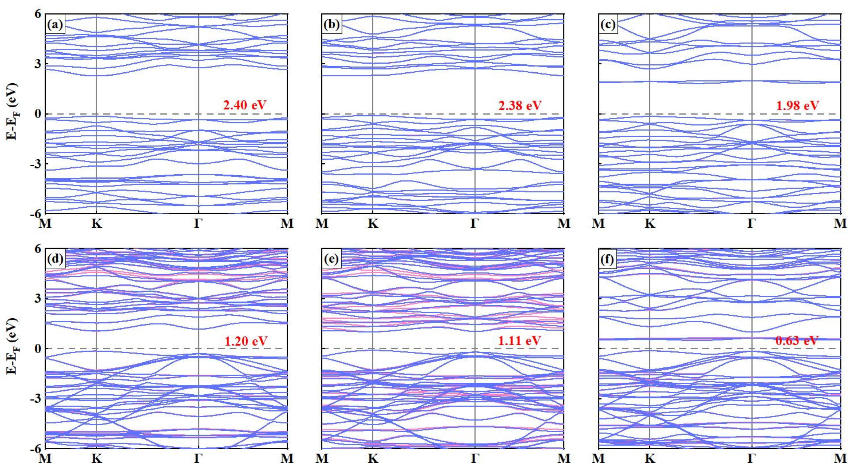
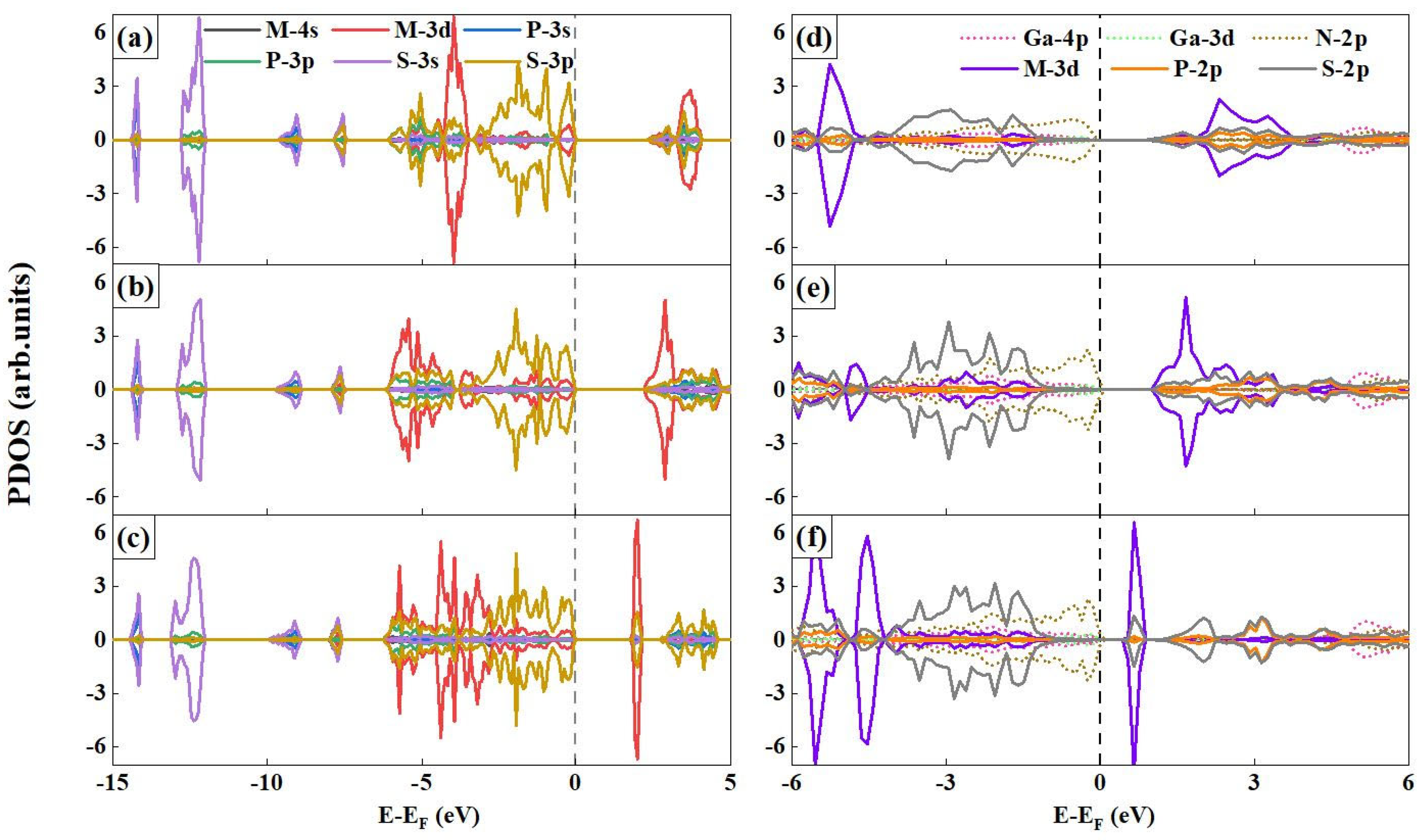
3.3. Electronic Properties

Figure 3a–c presents the band structures of the MPS3 MLs, where it has been found that their ground states are AFM semiconductors with nearly degenerate energy bands in the spin-up and spin-down channels. Specifically, for the MnPS3 ML, having both the conduction band minimum (CBM) and the valence band maximum (VBM) located at the K point in the Brillouin zone indicates a direct band gap, meaning that electron transitions between the valence band and the conduction band can occur with minimal momentum change, whereas the FePS3 ML exhibits an indirect band gap with the CBM between the M and K points and the VBM solely at the K point. The NiPS3 ML, as an indirect band gap material with its CBM between the K and Γ points and the VBM remaining at the K point, has intermediate states of Ni-3d and S-3p within its energy gap that significantly reduce its band gap (as shown in Figure 4c), and in the indirect band gap of NiPS3 ML, the optical absorption or emission processes involve simultaneous changes in energy and momentum. We further confirmed these findings through the HSE06 method (shown in Figure S1, Supporting Materials), and understanding the band structure characteristics of these materials is crucial for tailoring their electrical, optical, and optoelectronic properties to meet specific application requirements. To gain a more in-depth understanding of their electronic properties, we calculated the projected density of states (PDOS) (results shown in Figure 4a–c), and the fact that the Fermi levels (EF) of the three MPS3 MLs structures overlap with the VBM indicates that these materials possess specific electronic properties such as a filled valence bands and low electrical conductivity. The S-3p and M-3d states were found to make significant contributions to the VBM, suggesting their crucial role in determining electronic behavior near the VBM, while the CBM is mainly occupied by the M-3d states, indicating that the electron transitions responsible for charge transport and conductivity involve the participation of these specific orbitals. Moreover, in the three MPS3 MLs, the tendency of the M-3d states to get closer to the EF leads to a gradual decrease in the band gap, a phenomenon that can be attributed to the localized nature of the M-3d states playing an important role in narrowing band gaps as they increase the electronic density of states near the EF and thus reduce the energy separation between the VBM and the CBM.
The electronic structure of vdWHs was investigated through comparative analysis of their constituent MPS3 MLs, revealing significant bandgap reductions of 50.00%, 53.16%, and 68.18% in MnPS3/GaN, FePS3/GaN, and NiPS3/GaN heterostructures, respectively, with corresponding BL bandgaps decreasing to 1.20 eV, 1.11 eV, and 0.63 eV compared to their MLs counterparts (2.40 eV, 2.37 eV, and 1.98 eV). This substantial bandgap narrowing arises from interfacial interactions and modified band alignment, where the EF shifts upward away from the VBM of MPS3 MLs, allowing GaN ML to dominate the VBM through its N atoms while the CBM remains governed by the antiferromagnetic MPS3 MLs, thereby establishing a type-II band alignment that spatially separates charge carriers across layers. Notably, MnPS3/GaN and FePS3/GaN vdWHs exhibit direct bandgaps with VBM and CBM localized at the K-point, whereas NiPS3/GaN vdWHs shows reversed alignment with Γ-point VBM and a CBM positioned between K-Γ points, with all systems demonstrating hybridization between GaN-derived N-2p and M-3d states at the interface. This unique electronic configuration facilitates the formation of interlayer excitons through spatial charge separation, suggesting enhanced potential for optoelectronic applications requiring efficient charge transfer mechanisms.

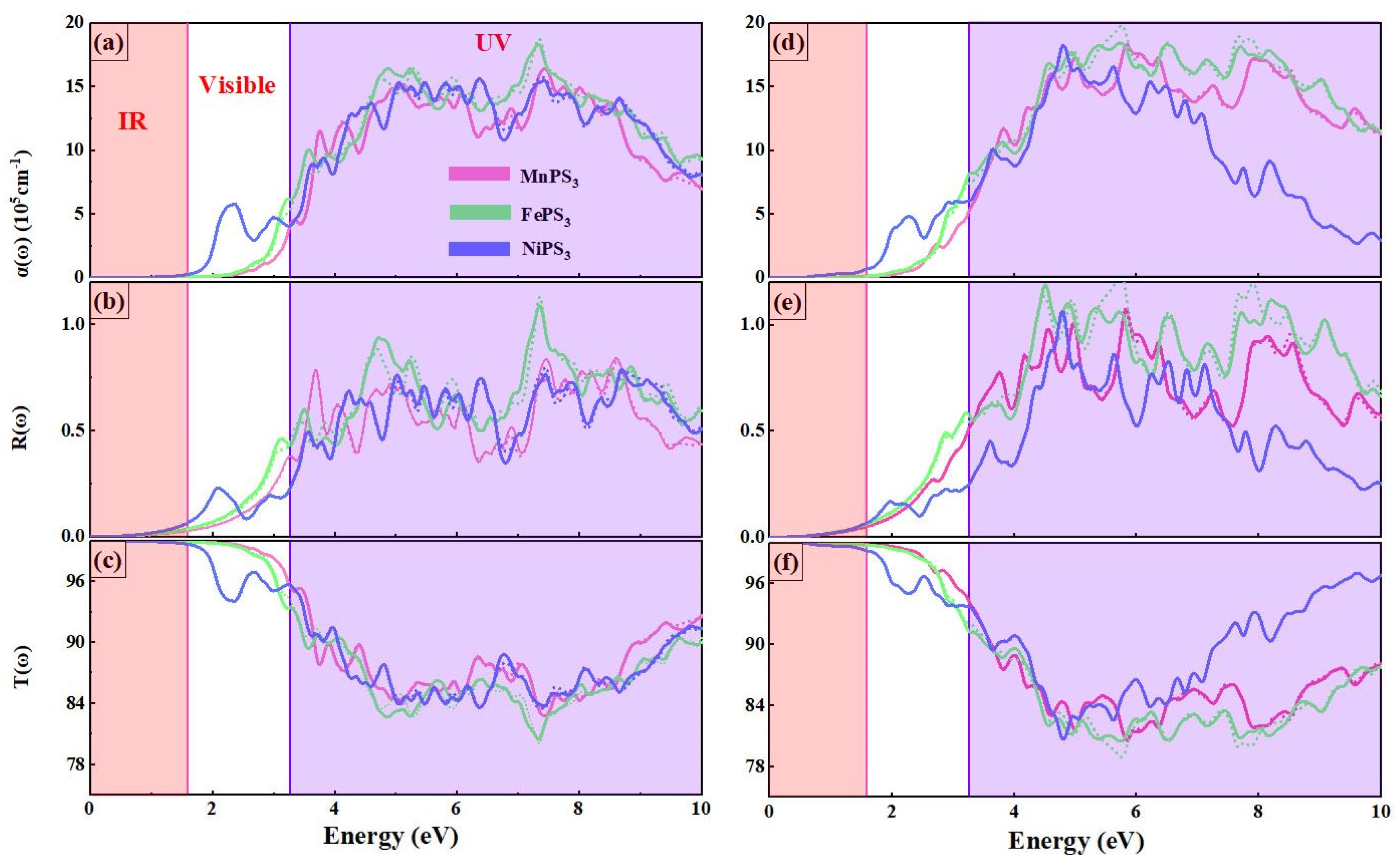
3.4. Optical Properties

The complex dielectric function is a crucial parameter for characterizing the optical properties of materials. It describes the linear response of materials to incident radiation (ε(ω) = ε1(ω) + iε2(ω)). Here, ε1(ω) and ε2(ω) represent the scattering of radiation within the material and the absorption of radiation by the material, respectively. The ε2(ω) spectrum can be calculated from the energy band dispersion, and ε1(ω) can be derived from ε2(ω) through the Kramers–Kronig transformation. Based on the complex dielectric function ε(ω), other optical functions can also be predicted, such as the absorption coefficient α(ω), reflectivity R(ω), and transmission T(ω) coefficient [41,42]. The optical absorption of MPS3/GaN vdW heterostructures is investigated by computing the complex dielectric function: ε(ω) = ε1(ω) + ε2(ω), where the imaginary part ε2(ω) is related to the absorption at a specific frequency ω, and the real part ε1(ω) is obtained from ε2(ω) using the Kramers–Kronig relation. The absorption spectrum can be calculated 1using the following formula:
α ω   = 2 ω ch ε 1 2 + ε 2 2 ε 1 2 1 2
where c is the speed of light in a vacuum. Strong anisotropy is observed in the absorption spectra α(ω) of MPS3 MLs and MPS3/GaN vdWHs along two polarization directions. The absorption coefficient is equal to the number of light leaps per unit volume.
Note that these spectra were calculated for incident radiation polarized parallel and perpendicular to the crystallographic directions. MPS3 MLs maintain optical isotropy in the specified energy range (0–3.29 eV), meaning that their absorption characteristics are uniform in all directions. This property is advantageous for applications requiring consistent optical performance, such as in optoelectronic devices. FePS3 and NiPS3 MLs display weak anisotropy at higher energies. This behavior can be attributed to their unique electronic structures and magnetic interactions, which lead to directional variations in optical absorption. From Figure 5a–c, it can be clearly observed that all three materials exhibit high sensitivity to the UV region and have a significant response intensity (on the order of 106). This large response intensity indicates that these materials possess high-efficiency light absorption in the UV region, making them potentially valuable for UV detection or UV-based optoelectronic devices. In contrast, the absorption response of the NiPS3 ML is particularly prominent in the visible light region, with an absorption peak at around 2.3 eV. This suggests that NiPS3 ML has a smaller bandgap, enabling it to absorb visible light more effectively. This characteristic endows NiPS3 ML with a unique advantage in applications that require visible light absorption, such as in photovoltaics or photocatalysis. As shown in Figure 5d–f, the overall trend of the MPS3/GaN vdWHs curve exhibits a relatively weak change under the influence of the GaN ML, indicating that the GaN ML has a relatively minor impact on the electronic structure of the heterostructure. This may be due to the high stability and wide bandgap of the GaN ML itself, which limits its interaction with the host material. However, the red shift of the light absorption edge is a significant finding, indicating that the optical properties of the GaN ML have changed. This red shift is usually associated with a reduction in the bandgap, enabling the material to absorb photons with longer wavelengths. The introduction of the GaN ML opens up new possibilities for designing vdWHs with specific optical properties. By adjusting the bandgap and absorption range, researchers can optimize the performance of these materials in specific applications, such as improving the efficiency of photovoltaic devices or enhancing the performance of photocatalytic reactions.

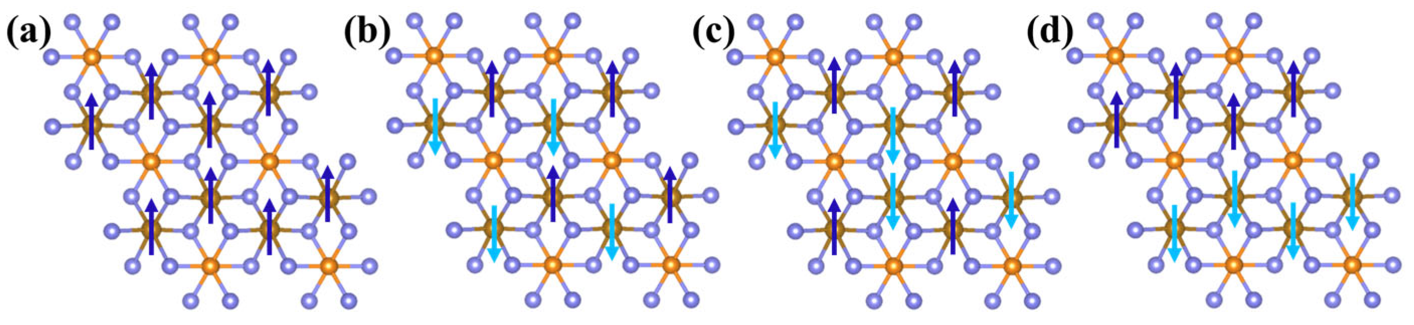
3.5. Magnetic Properties

To further explore the magnetic mechanism of the system, 2 × 2 × 1 supercells were constructed (Figure 6) and four magnetic configurations were considered: (a) FM, (b) Néel AFM, (c) stripy AFM, and (d) zigzag AFM. It was found that in MnPS3 and NiPS3 MLs, the Néel-type antiferromagnetic order is energetically favored, while FePS3 exhibits a Zigzag-type antiferromagnetic order (as shown in Table 2). Specifically, the values for MPS3 MLs ground states are −279.73, −191.88, and −281.39 meV, respectively. These negative values unequivocally confirm the AFM nature of these structures. The magnetic moments contributed by each M (M = Mn, Fe, and Ni) atoms are 4.498, 3.672, and 1.517 μ B , respectively. Further testing revealed that the magnetic moments of these three structures are predominantly contributed by the M-3d states, accounting for 98.63%, 98.69%, and 99.87% of the total magnetic moment, respectively. This observation is closely related to the electronic configurations of transition metals (e.g., Mn: 3d5, Fe: 3d6, and Ni: 3d8), where the spin polarization of unpaired electrons in the 3d orbitals serves as the primary contributor to the magnetic moments, exhibiting strong localization characteristics (as shown in Figure 4d–f). Interestingly, in the vdWHs, the △E of the MPS3 MLs become −62.63, −54.30, and −55.21 eV, respectively. The magnetic moments of each M atom are 4.541 μ B for Mn, 3.659 μ B for Fe, and 1.489 μ B for Ni. Upon forming vdWHs, the total energies decrease to −152.81, −90.39, and −178.82 eV, while the magnetic moments increase to 4.586, 3.677, and 1.564 μ B . The data show that compared to MPS3 MLs, the △E in vdWHs has increased by 45.37%, 52.89%, and 36.45%, respectively, while the MM has increased by 0.99%, 0.49%, and 5.04%. These changes indicate that the magnetic properties of the system have been significantly altered upon the formation of the van der Waals heterobilayer structure. To further validate their magnetic properties, we explored three distinct computational approaches: with and without considering van der Waals forces and the other with spin-orbit coupling (SOC) included (see Table S3). The results from both methods consistently align with the trends observed in the above analysis. The interlayer van der Waals interactions may induce hybridization between the M-3d orbitals and neighboring p/d states, thereby enhancing spin polarization. For instance, the 3d8 configuration of Ni demonstrates heightened sensitivity to interlayer charge transfer, resulting in the largest magnetic moment enhancement.
Moreover, the magnetocrystalline anisotropy energy (MAE) has been calculated to determine the preferred magnetization directions in MPS3 MLs [43,44,45]. This study investigated the magnetic orientation characteristics of MPS3 MLs and their vdWHs by calculating the MAE. Specifically, using the total energy difference between the in-plane [010] direction (corresponding to Cartesian axis b) and the out-of-plane [001] direction (corresponding to axis c) as the criterion (MAE = Ey − Ez), the MAE values for the three types of MPS3 MLs were determined to be −0.33, 10.14, and 1.33 meV, respectively. Notably, two of the ML materials exhibited negative MAE values, indicating a lower energy advantage for the in-plane orientation. However, when configured into vdWHs MAE values significantly weakened, decreasing to −0.34, −3.59, and 0.15 meV, respectively. A sign reversal in the MAE of the second material group suggests that interlayer interactions may drive a transition in magnetic anisotropy from in-plane dominance to an out-of-plane preference. This comparative analysis highlights the regulatory role of interlayer coupling in two-dimensional materials on magnetic anisotropy, offering critical insights for the design of magnetic devices based on MPS3 systems.

4. Discussion

This study focuses on the two-dimensional antiferromagnetic materials MPS3 MLs (M = Mn, Fe, and Ni) and their vdWHs structures formed with GaN MLs, which have gradually attracted attention in the field of spintronics. Through first-principles calculations, we systematically studied the structural stability, charge transfer, band structure, density of states, optical properties, and magnetic properties of these materials, and explored their potential applications in optoelectronics and spintronics. By analyzing the phonon spectra, we confirmed the dynamic stability of the MPS3 MLs and conducted a detailed analysis of their bond lengths, charge distributions, and wide-bandgap semiconductor properties. In addition, based on the optical absorption spectra, reflectance, and transmittance, we explored the potential applications of the MPS3 MLs in the field of ultraviolet detection. The construction of the MPS3/GaN vdWHs led to a significant reduction in the bandgap (changing from 2.40, 2.38, and 1.98 to 1.20, 1.11, and 0.63), thus expanding the potential application range of its optical properties to the visible light region. Through calculations, we confirmed the intrinsic antiferromagnetic properties of the MPS3 MLs and determined the magnetic moments of the magnetic atoms M to be 4.560, 3.672, and 1.517 μB, respectively. The vdWHs structure further enhanced the magnetic moments of these elements. We conducted a further analysis of the magnetic properties of the MPS3 MLs and vdWHs using SOC and confirmed their magnetic anisotropy. These results provide a solid theoretical basis for the design of novel two-dimensional spintronic and optoelectronic devices based on MPS3.

Supplementary Materials

The following supporting information can be downloaded at: https://www.mdpi.com/article/10.3390/nano15110832/s1.

Author Contributions

Methodology, L.H., K.Z., M.J., H.X. and X.C.; Validation, J.W.; Investigation, S.L., X.L. and Y.Z.; Resources, A.L. and Y.H.; Writing—original draft, S.T.; Writing—review & editing, L.H., L.Z., H.X. and X.C. All authors have read and agreed to the published version of the manuscript.

Funding

This research was funded by the Fundamental Research Funds for the Central Universities (2232022A-11), the Fundamental Research Funds from the Central Universities and Graduate Student Innovation Fund of Donghua University (CUSF-DH-D-2022074), the China Postdoctoral Science Foundation (No. 2024M750694), and the computational support from the Shanghai Supercomputer Center, the National Natural Science Foundation of Shanghai (21ZR1402200).

Data Availability Statement

No data were used for the research described in the article.

Conflicts of Interest

The authors declare that they have no known competing financial interests or personal relationships that could have appeared to influence the work reported in this article.

References

  1. Novoselov, K.S.; Geim, A.K.; Morozov, S.V.; Jiang, D.; Zhang, Y.; Dubonos, S.V.; Grigorieva, I.V.; Firsov, A.A. Electric Field Effect in Atomically Thin Carbon Films. Science 2004, 306, 666–669. [Google Scholar] [CrossRef] [PubMed]
  2. Ha, C.; Chung, Y.J. Thin films as practical quantum materials: A status quo and beyond. APL Mater. 2024, 12, 120901. [Google Scholar] [CrossRef]
  3. Boschker, H.; Mannhart, J. Quantum-Matter Heterostructures. Annu. Rev. Condens. Matter Phys. 2017, 8, 145–164. [Google Scholar] [CrossRef]
  4. Geim, A.K.; Grigorieva, I.V. Van der Waals Heterostructures. Nature 2013, 499, 419–425. [Google Scholar] [CrossRef] [PubMed]
  5. Butler, S.Z.; Hollen, S.M.; Cao, L.; Cui, Y.; Gupta, J.A.; Gutiérrez, H.R.; Heinz, T.F.; Hong, S.S.; Huang, J.; Ismach, A.F.; et al. Progress, Challenges, and Opportunities in Two-Dimensional Materials Beyond Graphene. ACS Nano 2013, 7, 2898–2926. [Google Scholar] [CrossRef]
  6. Gong, C.; Li, L.; Li, Z.; Ji, H.; Stern, A.; Xia, Y.; Cao, T.; Bao, W.; Wang, C.; Wang, Y.; et al. Discovery of Intrinsic Ferromagnetism in Two-Dimensional van der Waals Crystals. Nature 2017, 546, 265–269. [Google Scholar] [CrossRef]
  7. Burch, K.S.; Mandrus, D.; Park, J.G. Magnetism in Two-Dimensional van der Waals Materials. Nature 2018, 563, 47–52. [Google Scholar] [CrossRef] [PubMed]
  8. Huang, B.; Clark, G.; Navarro-Moratalla, E.; Klein, D.R.; Cheng, R.; Seyler, K.L.; Zhong, D.; Schmidgall, E.; McGuire, M.A.; Cobden, D.H.; et al. Layer-dependent ferromagnetism in a van der Waals crystal down to the monolayer limit. Nature 2017, 546, 270–273. [Google Scholar] [CrossRef]
  9. Zhang, B.; Lu, P.; Tabrizian, R.; Feng, P.X.; Wu, Y. 2D Magnetic heterostructures: Spintronics and quantum future. NPJ Spintron. 2024, 2, 6. [Google Scholar] [CrossRef]
  10. Samarth, N. Magnetism in flatland. Nature 2017, 546, 216–217. [Google Scholar] [CrossRef]
  11. Ohno, H.; Chiba, D.; Matsukura, F.; Omiya, T.; Abe, E.; Dietl, T.; Ohno, Y.; Ohtani, K. Electric-field control of ferromagnetism. Nature 2000, 408, 944–946. [Google Scholar] [CrossRef] [PubMed]
  12. Han, W.; Kawakami, R.K.; Gmitra, M.; Fabian, J. Graphene spintronics. Nat. Nanotechnol. 2014, 9, 794–807. [Google Scholar] [CrossRef] [PubMed]
  13. Brec, R. Review on structural and chemical properties of transition metal phosphorous trisulfides MPS3. Solid State Ion. 1986, 22, 3–30. [Google Scholar] [CrossRef]
  14. Rule, K.C.; McIntyre, G.J.; Kennedy, S.J.; Hicks, T.J. Single-crystal and powder neutron diffraction experiments on FePS3: Search for the magnetic structure. Phys. Rev. B—Condens. Matter Mater. Phys. 2007, 76, 134402. [Google Scholar] [CrossRef]
  15. Susner, M.A.; Chyasnavichyus, M.; McGuire, M.A.; Ganesh, P.; Maksymovych, P. Metal Thio- and Selenophosphates as Multifunctional van der Waals Layered Materials. Adv. Mater. 2017, 29, 1602852. [Google Scholar] [CrossRef] [PubMed]
  16. Rahman, S.; Torres, J.F.; Khan, A.R.; Lu, Y. Recent Developments in van der Waals Antiferromagnetic 2D Materials: Synthesis, Characterization, and Device Implementation. ACS Nano 2021, 15, 17175–17213. [Google Scholar] [CrossRef]
  17. Joy, P.A.; Vasudevan, S. Magnetism in the layered transition-metal thiophosphates MPS3 (M = Mn, Fe, and Ni). Phys. Rev. B 1992, 46, 5425–5433. [Google Scholar] [CrossRef]
  18. Kim, H.-S.; Haule, K.; Vanderbilt, D. Mott Metal-Insulator Transitions in Pressurized Layered Trichalcogenides. Phys. Rev. Lett. 2019, 123, 236401. [Google Scholar] [CrossRef]
  19. Kim, S.Y.; Kim, T.Y.; Sandilands, L.J.; Sinn, S.; Lee, M.-C.; Son, J.; Lee, S.; Choi, K.-Y.; Kim, W.; Park, B.-G.; et al. Charge-Spin Correlation in van der Waals Antiferromagnet NiPS3. Phys. Rev. Lett. 2018, 120, 136402. [Google Scholar] [CrossRef]
  20. Li, Y.; Wu, X.; Gu, Y.; Le, C.; Qin, S.; Thomale, R.; Hu, J. Topological superconductivity in Ni-based transition metal trichalcogenides. Phys. Rev. B 2019, 100, 214513. [Google Scholar] [CrossRef]
  21. Novoselov, K.S.; Mishchenko, A.; Carvalho, A.; Castro Neto, A.H. 2D materials and van der Waals heterostructure. Science 2016, 353, aac9439. [Google Scholar] [CrossRef]
  22. Meftakhutdinov, R.M.; Sibatov, R.T.; Kochaev, A.I.; Evseev, D.A. First-principles study of graphenylene/MoX2 (X = S, Te, and Se) van der Waals heterostructures. Phys. Chem. Chem. Phys. 2021, 23, 14315–14324. [Google Scholar] [CrossRef] [PubMed]
  23. Ng, J.Q.; Wu, Q.; Ang, L.K.; Ang, Y.S. Tunable electronic properties and band alignments of MoSi2N4/GaN and MoSi2N4/ZnO van der Waals heterostructures. Appl. Phys. Lett. 2022, 120, 103101. [Google Scholar] [CrossRef]
  24. Peng, B.; Xu, L.; Zeng, J.; Qi, X.; Yang, Y.; Ma, Z.; Huang, X.; Wang, L.-L.; Shuai, C. Layer-dependent photocatalysts of GaN/SiC-based multilayer van der Waals heterojunctions for hydrogen evolution. Catal. Sci. Technol. 2021, 11, 3059–3069. [Google Scholar] [CrossRef]
  25. Rehman, G.; Khan, S.A.; Amin, B.; Ahmad, I.; Gan, L.-Y.; Maqbool, M. Intriguing electronic structures and optical properties of two-dimensional van der Waals heterostructures of Zr2CT2 (T = O, F) with MoSe2 and WSe2. J. Mater. Chem. C 2018, 6, 2830–2839. [Google Scholar] [CrossRef]
  26. Wang, Z.; Zhu, W. Tunable Band Alignments in 2D Ferroelectric α-In2Se3 Based Van der Waals Heterostructures. ACS Appl. Electron. Mater. 2021, 3, 5114–5123. [Google Scholar] [CrossRef]
  27. Yuan, H.; Su, J.; Zhang, S.; Di, J.; Lin, Z.; Zhang, J.; Zhang, J.; Chang, J.; Hao, Y. Interfacial transport modulation by intrinsic potential difference of janus TMDs based on CsPbI3/J-TMDs heterojunctions. Iscience 2022, 25, 103872. [Google Scholar] [CrossRef]
  28. Zhang, M.; Si, R.; Wu, X.; Dong, Y.; Fu, K.; Xu, X.; Zhang, J.; Li, L.; Guo, Y. Two-dimensional Hf2CO2/GaN van der Waals heterostructure for overall water splitting: A density functional theory study. J. Mater. Sci. Mater. 2021, 32, 19368–19379. [Google Scholar] [CrossRef]
  29. Zhou, B.; Gong, S.J.; Jiang, K.; Xu, L.; Zhu, L.; Shang, L.; Li, Y.; Hu, Z.; Chu, J. Ferroelectric and dipole control of band alignment in the two dimensional InTe/In2Se3 heterostructure. J. Phys. Condens. Matter. 2020, 32, 055703. [Google Scholar] [CrossRef]
  30. Zhou, B.; Jiang, K.; Shang, L.; Zhang, J.; Li, Y.; Zhu, L.; Gong, S.-J.; Hu, Z.; Chu, J. Enhanced carrier separation in ferroelectric In2Se3/MoS2 van der Waals heterostructures. J. Mater. Chem. C 2020, 8, 11160–11167. [Google Scholar]
  31. Zhu, J.; Ning, J.; Wang, D.; Zhang, J.; Guo, L.; Hao, Y. Tunable band offset in black Phosphorus/ReS2 van der Waals heterostructure with robust direct band and inherent anisotropy. Superlattices Microstruct. 2019, 129, 274–281. [Google Scholar] [CrossRef]
  32. Kresse, G.; Joubert, D. From ultrasoft pseudopotentials to the projector augmented-wave method. Phys. Rev. B 1999, 59, 1758–1775. [Google Scholar] [CrossRef]
  33. Kresse, G.; Furthmüller, J. Efficient iterative schemes for ab initio total-energy calculations using a plane-wave basis set. Phys. Rev. B 1996, 54, 11169–11186. [Google Scholar] [CrossRef] [PubMed]
  34. Blochl, P.E. Projector augmented-wave method. Phys. Rev. B 1994, 50, 17953. [Google Scholar] [CrossRef]
  35. Perdew, J.P.; Burke, K.; Ernzerhof, M. Generalized Gradient Approximation Made Simple. Phys. Rev. Lett. 1996, 77, 3865–3868. [Google Scholar] [CrossRef]
  36. Ernzerhof, M.; Scuseria, G.E. Assessment of the Perdew–Burke–Ernzerhof exchange-correlation functional. J. Chem. Phys. 1999, 110, 5029–5036. [Google Scholar] [CrossRef]
  37. Setyawan, W.; Gaume, R.M.; Lam, S.; Feigelson, R.S.; Curtarolo, S. High-throughput combinatorial database of electronic band structures for inorganic scintillator materials. ACS Comb. Sci. 2011, 13, 382–390. [Google Scholar] [CrossRef]
  38. Wu, R.; Freeman, A.J. Spin–orbit induced magnetic phenomena in bulk metals and their surfaces and interfaces. J. Magn. Magn. Mater. 1999, 200, 498–514. [Google Scholar] [CrossRef]
  39. Tian, S.; Zhang, L.; Liang, Y.; Xie, R.; Hna, L.; Lan, S.; Lu, A.; Huang, Y.; Xing, H.; Chen, X. Room Temperature Ferromagnetic Properties of Ga14N16-nGd2Cn Monolayers: A First Principle Study. Crystals 2023, 13, 531. [Google Scholar] [CrossRef]
  40. Attia, A.A.; Jappor, H.R. Tunable electronic and optical properties of new two-dimensional GaN/Bas van der Waals heterostructures with the potential for photovoltaic applications. Chem. Phys. Lett. 2019, 728, 124–131. [Google Scholar] [CrossRef]
  41. Wang, G.; Zhou, F.; Yuan, B.; Xiao, S.; Kuang, A.; Zhong, M.; Dang, S.; Long, X.; Zhang, W. Strain-Tunable Visible-Light-Responsive Photocatalytic Properties of Two-Dimensional CdS/g-C3N4: A Hybrid Density Functional Study. Nanomaterials 2019, 9, 244. [Google Scholar] [CrossRef] [PubMed]
  42. Wang, X.; Wu, R.; Wang, D.-s.; Freeman, A.J. Torque method for the theoretical determination of magnetocrystalline anisotropy. Phys. Rev. B 1996, 54, 61. [Google Scholar] [CrossRef] [PubMed]
  43. Hosseini, S.M.; Movlarooy, T.; Kompany, A. First-principles study of the optical properties of PbTiO3. Eur. Phys. J. B-Condens. Matter Complex Syst. 2005, 46, 463–469. [Google Scholar] [CrossRef]
  44. Milman, V.; Warren, M.C. Elastic properties of TiB2 and MgB2. J. Phys. Condens. Matter 2001, 13, 5585. [Google Scholar] [CrossRef]
  45. Grimme, S.; Antony, J.; Ehrlich, S.; Krieg, H. A consistent and accurate ab initio parametrization of density functional dispersion correction (DFT-D) for the 94 elements H-Pu. J. Chem. Phys. 2010, 132, 154104. [Google Scholar] [CrossRef]
Figure 1. (a) The top and side view in atomic level for MPS3 MLs and vdWHs, the phonon dispersion for (b) MnPS3, (c) FePS3, and (d) NiPS3 MLs.
Nanomaterials 15 00832 g001
Figure 2. Top views of the ELF of the MPS3 MLs and vdWHs with the isosurface levels set at 0.45.
Nanomaterials 15 00832 g002
Figure 3. Band structure of MPS3 MLs and vdWHs: (a) MnPS3 MLs, (b) FePS3 MLs, (c) NiPS3 MLs, (d) MnPS3/GaN vdWs, (e) FePS3/GaN vdWs, and (f) NiPS3/GaN vdWs. The fermi level (EF) is marked in dashed lines. The bandgaps are listed in the corresponding pictures. The pink and blue lines represent the spin-up and spin-down channels, respectively.
Nanomaterials 15 00832 g003
Figure 4. The projected density of states (PDOS) of MPS3 MLs and vdWHs: (a) MnPS3 ML, (b) FePS3 ML, (c) NiPS3 ML, (d) MnPS3/GaN vdWs, (e) FePS3/GaN vdWs, and (f) NiPS3/GaN vdWs. The Fermi level (EF) is marked in dashed lines.
Nanomaterials 15 00832 g004
Figure 5. Calculated spectra of the (a) adsorption α(ω), (b) reflection R(ω), and (c) transmission T(ω) coefficients of MPS3 MLs and (df) for MPS3/GaN vdWHs.
Nanomaterials 15 00832 g005
Figure 6. Geometric structures of four different magnetic configurations. (a) FM order, (b) Néel AFM order, (c) Stripy AFM order, and (d) Zigzag AFM order.
Nanomaterials 15 00832 g006
Table 1. The lattice parameter; energy difference (△E); binding energy (Eb); bond length between M and M atoms (dM-M); P and S atoms (dP-S); P and P atoms (dP-S) for relaxed MPS3 MLs and MPS3/GaN vdWHs; and the calculated charge transfer (CT) of M, P, and S atoms in MPS3 MLs and MPS3/GaN vdWHs.
Lattice Parameters
(Å)
Bond Length
(Å)
CT
(|e|)
△E
(meV)
E
b(eV)
abdM-MdP-SdP-PMPS
MPS3 MLs
MnPS36.136.133.542.042.21−1.191−0.9790.723−59.57
FePS36.006.033.422.052.20−1.065−0.9700.678−52.51
NiPS35.895.893.392.042.18−0.7750.9750.583−55.21
vdWH BLs
MnPS36.316.313.652.052.19−1.226−0.9520.731−44.81−0.566
FePS36.276.273.592.062.18−1.085−0.9270.676−17.44−0.571
NiPS36.246.233.602.072.16−0.825−0.8950.580−25.91−0.591
Table 2. The energy difference △E-Néel (△E-N), △E-Stripy (△E-S), and △E-Zigzag (△E-Z) and the magnetic moment of per M atoms and M-d states in MPS3 MLs and MPS3/GaN vdWHs.
MPS3 MLsvdWHs
MMnFeNiMnFeNi
△E-N (meV)−279.73−165.96−238.98−152.81−68.56−162.27
△E-S (meV)−158.15−40.3059.49−26.84−34.1641.95
△E-Z (meV)−166.25−191.88−281.39−102.59−90.39−178.82
MM ( μ B )4.5413.6591.4894.5863.6771.564
MM-d ( μ B )4.4793.6111.4874.5243.6271.558
MAE (meV)−0.3310.14−1.33−0.34−3.590.15
Disclaimer/Publisher’s Note: The statements, opinions and data contained in all publications are solely those of the individual author(s) and contributor(s) and not of MDPI and/or the editor(s). MDPI and/or the editor(s) disclaim responsibility for any injury to people or property resulting from any ideas, methods, instructions or products referred to in the content.

