Article

Rashba Spin Splitting in HgCdTe Quantum Wells with Inverted and Normal Band Structures

by
Svetlana V. Gudina
1,*,
Vladimir N. Neverov
1,
Mikhail R. Popov
1,
Konstantin V. Turutkin
1,
Sergey M. Podgornykh
1,
Nina G. Shelushinina
1,
Mikhail V. Yakunin
1,
Nikolay N. Mikhailov
2 and
Sergey A. Dvoretsky
2
1
M.N. Mikheev Institute of Metal Physics of Ural Branch of Russian Academy of Sciences, 620108 Yekaterinburg, Russia
2
A.V. Rzhanov Institute of Semiconductor Physics of Siberian Branch of Russian Academy of Sciences, 630090 Novosibirsk, Russia
*
Author to whom correspondence should be addressed.
Nanomaterials 2022, 12(7), 1238; https://doi.org/10.3390/nano12071238
Submission received: 3 March 2022 / Revised: 23 March 2022 / Accepted: 31 March 2022 / Published: 6 April 2022
(This article belongs to the Special Issue Advances in Semiconductor Nano-Structures)

Abstract

:
In quantum wells (QWs) formed in HgCdTe/CdHgTe heterosystems with a variable composition of Cd(Hg), Shubnikov-de-Haas (SdH) oscillations are investigated to characterize the Rashba-type spin-orbit coupling in QWs with both a normal and inverted band structure. Several methods of extracting the Rashba spin-splitting at zero magnetic field and their magnetic field dependences from the beatings of SdH oscillations are used for greater reliability. The large and similar Rashba splitting (25–27 meV) is found for different kinds of spectrum, explained by a significant fraction of the p-type wave functions, in both the E1 subband of the sample with a normal spectrum and the H1 subband for the sample with an inverted one.

1. Introduction

The main spin-dependent interaction in non-magnetic semiconductors is the spin-orbit interaction. Depending on the crystal symmetry, as well as on the structural properties of semiconductor heterostructures, the spin-orbit coupling takes different functional forms, providing a good selection of systems with different effective spin-orbit Hamiltonians. spin-orbit interaction leads to spin-splitting of energy levels in zero magnetic field for the states with sufficiently lowered symmetry, in both bulk (3D) systems and two-dimensional (2D) quantum wells.
The spin-orbit splitting of electron states in quantum wells (QWs) is usually discussed in terms of the Rashba spin-orbit coupling arising from the structure inversion asymmetry (SIA) of the 2D object [1,2,3,4], the Dresselhaus spin-orbit coupling arising due to the bulk inversion asymmetry in the noncentrosymmetric crystals and causing cubic k terms in the spectrum (the BIA contribution) [5,6,7], and the contribution from the inversion asymmetry of the interface (IIA) [8,9,10], as well as their combinations.
The idea of manipulating the charge carrier spin remains a hot topic in condensed matter physics; thus, the search for materials with prominent spin-dependent properties and the possibility of their improvement are of interest. The removal of spin degeneracy in the absence of a magnetic field is a topic of constant interest in the study of heterostructures based on narrow-gap and gapless semiconductors. The Rashba effect was studied in II–VI HgTe quantum wells, where the typical values of the Rashba splitting energy range from 17 meV [11] to 30 meV [12,13,14,15,16,17], which is noticeably larger than for the narrow-gap III–V systems (3–5 meV) (see, for example, [18] and references therein). In order to realize the spintronic device that operates at room temperature, the Rashba spin-splitting energy, ΔR, higher than thermal energy of 26 meV is desirable [19]. These are exactly the values that were obtained in structures based on the mercury telluride with an inverted band structure.
HgCdTe solid solutions contain heavy elements; therefore, they are semiconductors with a strong spin-orbit interaction [20,21]. CdTe has a positive band gap, so its band structure is similar to that of other conventional semiconductors. The conduction band states have s—symmetry (Γ6), and the states of the valence band have p—symmetry (Γ8). In the gapless semiconductor HgTe, due to relativistic effects [20], the Γ8 band normally forms the conduction band located above the Γ6 band, thus constituting an inverted band structure. An increase in the Cd content in the Hg1−xCdxTe solid solution causes a transition from an inverted to a normal band structure at x = 0.16 [21].
In the narrow HgTe quantum well within the Cd(Hg)Te/HgTe/Cd(Hg)Te heterostructure, two-dimensional electronic states have a normal band order (CdTe-like), but the sequence of the bands becomes inverted (HgTe-like) for d > dc, where dc is the critical width [22]. For HgTe/Cd0.7Hg0.3Te QWs grown on CdTe buffer, dc ≈ 6.5 nm. The critical width depends on the crystallographic orientation, buffer material and, especially, on the Cd content in Cd(Hg)Te solid solution in both the quantum well and the barriers. This provides an additional way of manipulating the properties of heterostructures with a HgTe (or CdHgTe) QW.
It is the inverted nature of HgTe band structure, i.e., the p-like character of energy states with the z-projection of total angular momentum Jz = ±3/2, that is responsible for the large Rashba spin-splitting. There are a few investigations of Rashba spin-splitting in HgTe QW with an inverted band order [11,12,13,14,23] that demonstrate a large spin-splitting. The triangle QWs in inversion layers on HgCdTe with normal [24] and inverted [15] band structures grown by the liquid-phase epitaxy technique were studied, and the latter demonstrated the record spin-splitting of 34 meV.
In Reference [25], the spectra of the cyclotron resonance in the classical and quantizing magnetic fields in asymmetric HgCdTe/CdHgTe heterostructures with selective doping in barriers were investigated. Self-consistent calculations of energy spectra (at B = 0) and Landau levels in a standard 8-band Kane model in Hartree approximation were performed. In low fields, a strong splitting of the cyclotron resonance line (10%), associated with the Rashba effect, was found in both a sample with an inverted band structure and a normal one. The evolution of absorption lines with a magnetic field of up to 34 T was traced when magnetic quantization prevailed over the Rashba splitting.
This paper presents the results of a thorough study of magnetotransport in Cd 1 x Hg x Te / Hg 1 t Cd t Te / Cd 1 y Hg y Te heterosystems with both an inverse band structure and a normal one, where the QWs are formed by different variations in the Cd (Hg) content. The original data demonstrating pronounced beatings of Shubnikov-de-Haas oscillations (SdH) and their scrupulous analysis are provided. The giant Rashba spin splittings and the dependence of total spin-splitting on the magnetic field are obtained through the Fourier analysis of oscillations and by analyzing the positions of the beating nodes in a magnetic field, respectively.

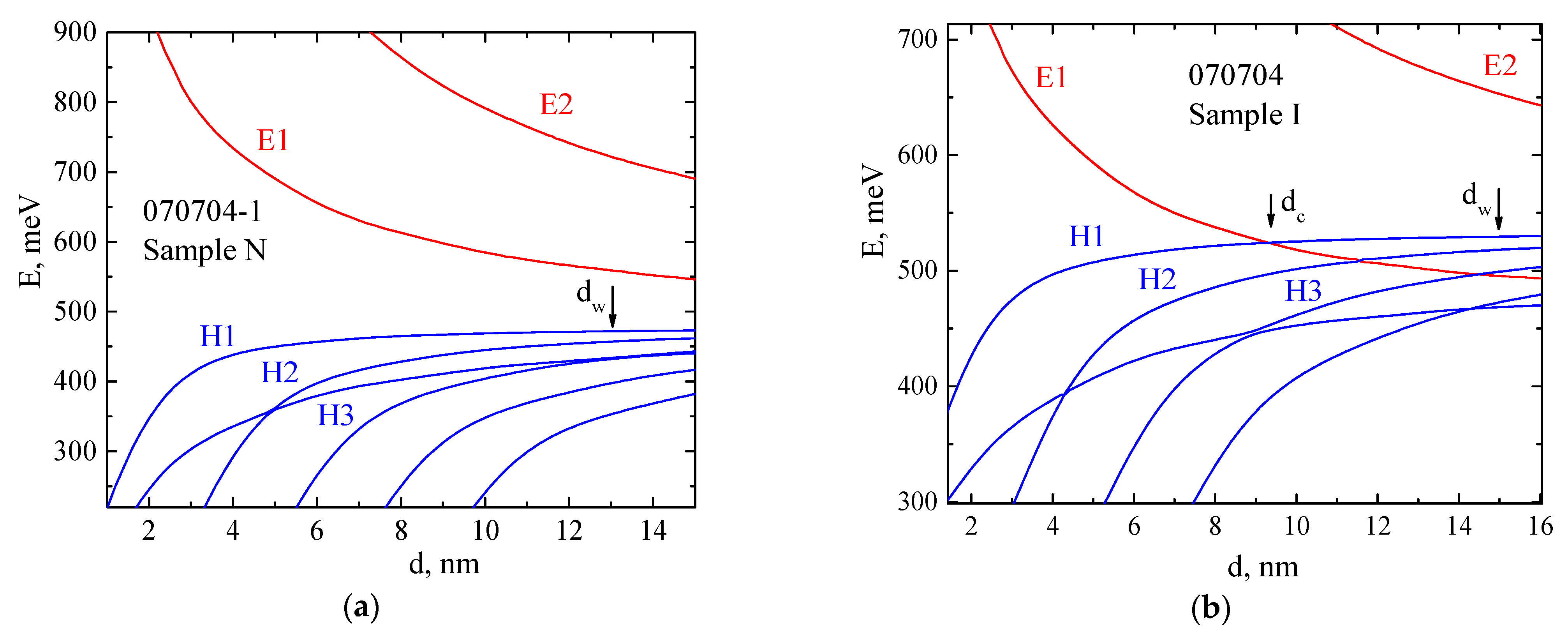
2. Materials and Methods
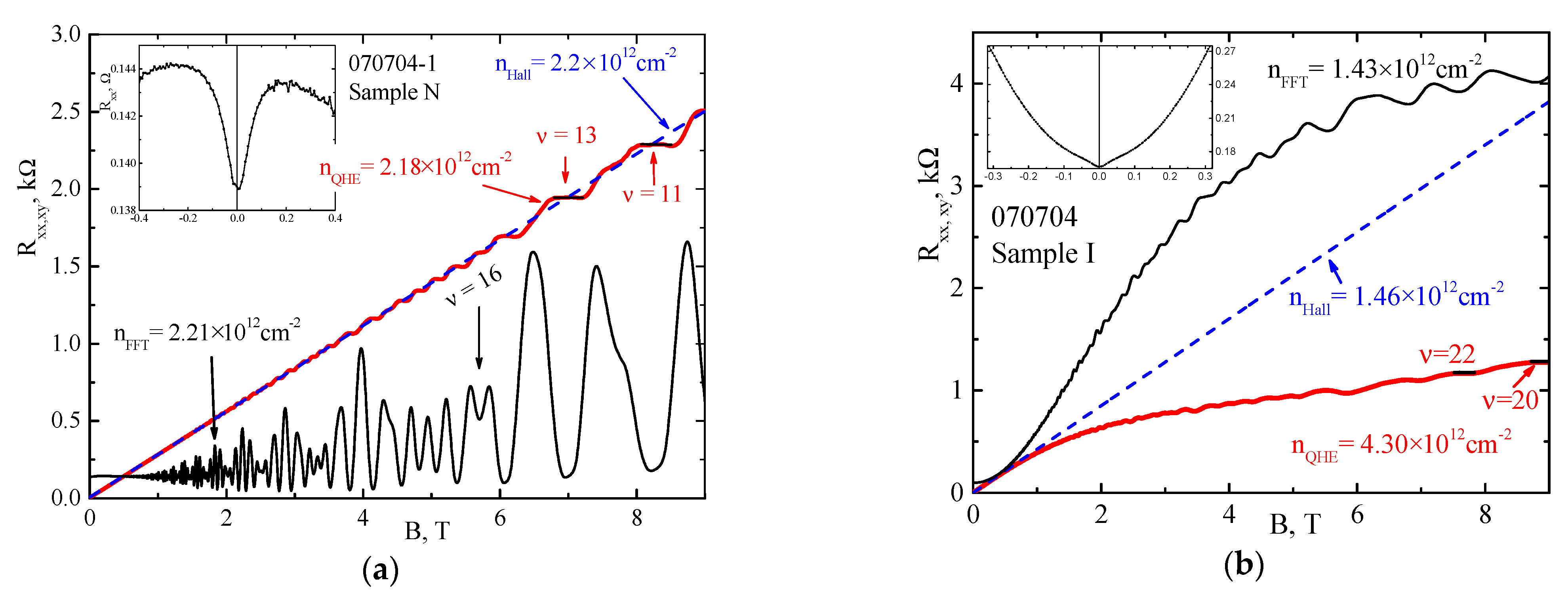
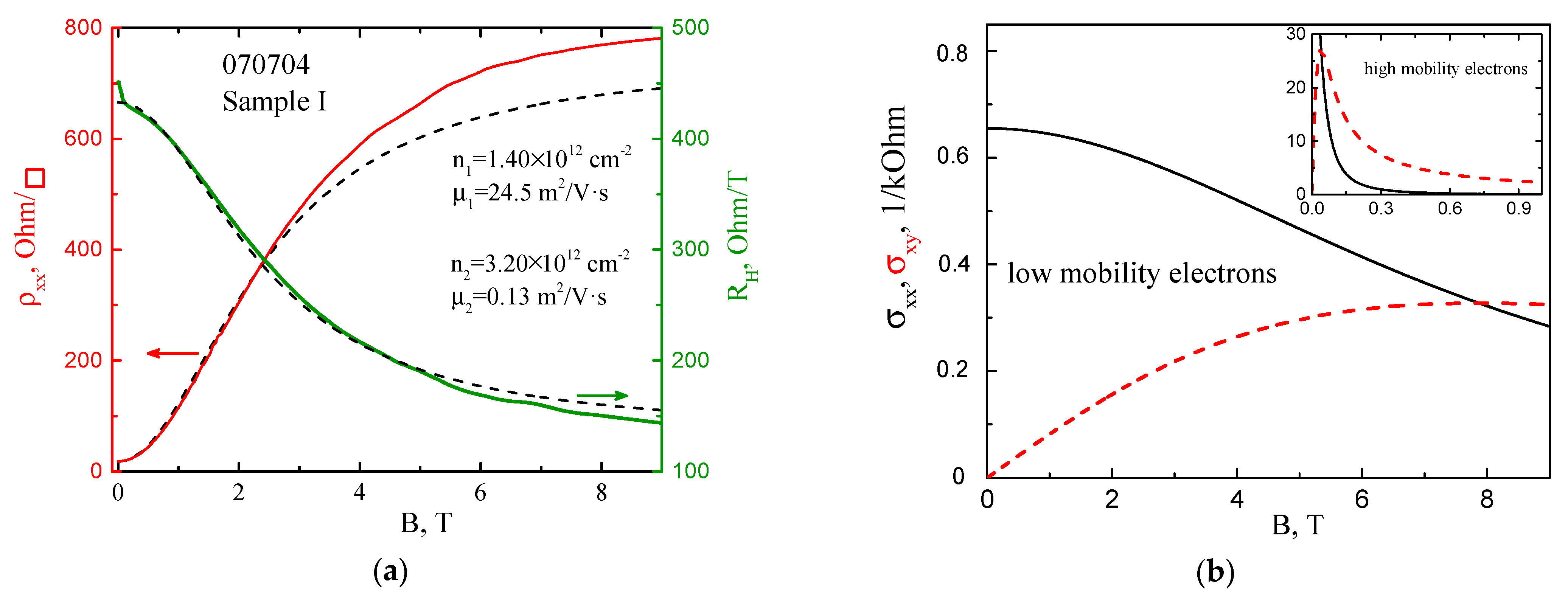
Our Cd 1 x Hg x Te / Hg 1 t Cd t Te / Cd 1 y Hg y Te QWs are grown by molecular beam epitaxy on GaAs (013) substrates [25,26,27,28,29]. The QWs are asymmetrically modulation doped with In in bottom barriers (on the substrate side), with a concentration nimp = 1.8 × 1018 cm−3. We measure two structures, which differ by various widths of the forming layers and by Cd(Hg) content. The first QW is Cd 0.89 Hg 0.11 Te / Hg 0.85 Cd 0.15 Te / Cd 0.85 Hg 0.15 Te (0.89/0.15/0.85) (Sample N), the second QW— Cd 0.6 Hg 0.4 Te / Hg 0.95 Cd 0.05 Te / Cd 0.53 Hg 0.47 Te (0.6/0.05/0.53) (Sample I). The Cd 1 x Hg x Te bottom barrier is composed of a spacer, a doped layer and one more barrier layer. Then, a buffering CdTe and ZnTe layers follow. Above QWs, there are a Cd 1 y Hg y Te barrier layer and a CdTe cap layer. The parameters of the sample structures are summarized in Table 1. Standard Hall bars are fabricated by wet chemical etching. Ohmic indium contacts are made by thermal soldering. Magnetotransport measurements are carried out in a He4 cryostat using DC techniques with a current of 1 μA in magnetic field B up to 9 T in Quantum Design measuring system and up to 12 T in Oxfords Instruments setup at temperature 1.8 K.
Cd 1 y Hg y Te Hg 1 t Cd t Te Cd 1 x Hg x Te Cd 1 x Hg x Te The calculations of the band structure for heterostructures close to those studied here both in composition and in the width of quantum wells were performed in [25] within the framework of the 8-band Kane model taking into account BIA and IIA. Structural asymmetry, due primarily to asymmetric doping, was taken into account in the Hartree approximation. The calculation showed the inverted type of band structure in Hg 0.95 Cd 0.05 Te QW, the lower subband in the conduction band is formed mainly by the states of heavy holes Γ8, in contrast to Hg 0.85 Cd 0.15 Te QW, which has a normal band order and the lower subband in the conduction band E1 of it is formed mainly by the electron-like states Γ6 (see Figure 1 and insets on it in [25]).
The calculation [25] predicts a significant Rashba spin splitting in the lower subband of the conduction band. Taking into account the BIA and IIA effects gives an additional correction to this value, and the contributions of these effects are significantly different in subbands of different nature. In the H1 band, the spin splitting increases by 1–2 meV, which is a small value vs the Rashba splitting background, but in the E2 subband these effects give a larger splitting of 2–3 meV.
Within the framework of the same calculation procedure, as in Reference [25], we calculated the dependence of the energies of size-quantized levels on the QW width in our structures (Figure 1). In Sample I (Figure 1b), the band inversion point is at a width of dc = 8.5 nm, which is much larger than the critical width for a classical quantum well Hg0.3Cd0.7Te/HgTe/Hg0.3Cd0.7Te (0.7/0/0.7) [22,30]. For Sample N, with a larger cadmium contents both in the QW and in the barriers, this point is hardly reached (Figure 1a).

3. Results

We analyze the components of the magnetoresistance tensor Rxx and Rxy measured in magnetic fields B up to 9 T at a fixed temperature T = 1.8 K. Both samples demonstrate a rich picture of SdH oscillations in magnetic fields from ~0.5 T to maximum fields of 9 T. However, the difference in the conductivity of the samples is also obvious. In Sample N, SdH oscillations are observed on the Rxx(B) dependence with a weak, almost linear, monotonic background (Figure 2a), while Sample I demonstrates a pronounced parabolic dependence of the longitudinal resistance in a magnetic field range up to 2 T, followed by a tendency towards saturation at B > 6 T (Figure 2b). The dependences of the Hall resistance Rxy on the magnetic field also significantly differ for the two samples. We reach the quantum Hall effect (QHE) plateaus with numbers, i = h/(e2Rxy), i = 11 (Sample N) and i = 20 (Sample I). Electron density, calculated from the position of the mentioned plateaus, are as follow: nQHE = 2.18 × 10¹⁶ m−2 (Sample N) and nQHE = 4.30 × 10¹⁶ m−2 (Sample I). For Sample N, we see the traditional QHE picture (red bold line in Figure 2a), in which the plateaus and the transition regions between them in the Rxy(B) dependence are centered around an inclined straight line, extrapolated from the classical Hall magnetoresistance in the low field region (blue dashed straight line in Figure 2a). Rxy(B) corresponds to the density of a two-dimensional electron gas nHall = 1/(RH × e) = 2.20 × 10¹⁶ m−2 (RH = Rxy(B)/B is the Hall constant), which is in excellent agreement with the QHE data. In Sample I, the deviation of the Rxy(B) dependence (red bold curve in Figure 2b) at B > 1 T from the classical Hall magnetoresistance (blue dashed straight line in Figure 2b) corresponds to the behavior of the Hall resistance for two types of electrons with different mobilities, as just seen for the Rxx behavior (see discussion in Appendix A). The electron density is nHall = 1/(RH×e) = 1.46 × 10¹⁶ m−2, which is almost three times less than the nQHE obtained from the QHE data.
A well-pronounced characteristic positive magnetoresistance is observed at very low perpendicular magnetic fields for both Sample N at B < 0.2 T and for Sample I at B << 0.1 T (see insets on Figure 2a,b, respectively), which is attributed to the effects of weak antilocalization (WAL). The WAL effect originates from the breaking of the spin coherence in magnetic fields in the presence of zero-field spin-splitting, ΔR, arising from the spin-orbit interaction. The discussion on WAL will be presented elsewhere.
Figure 3a for Sample N shows the dependence of Rxx on the filling factor ν, ν = ns/nB~1/B, where ns and nB = eB/h are the electron density and the number of states at the Landau level per unit area, respectively. The oscillations are periodic in the reciprocal magnetic field and have pronounced beating nodes. The positions of the Rxx (B) oscillation minima correspond to the integer values of the filling factor. To analyze the phases of the oscillations, we plot the dependence of the values of the reciprocal magnetic fields, 1/Bmin, corresponding to the oscillation minima, on the filling factor ν (inset in Figure 3a). It can be seen that the position of the oscillation beating node corresponds to a change in the parity of the filling factors (even and odd minima are indicated by different symbols, inset in Figure 3a). This change in the parity corresponds to a change by π of the oscillation phase, i.e., to a beating node. In quasi-classical terms, the presence of beats in the SdH oscillations indicates the existence of two close Fermi surfaces, which correspond to close values of oscillation frequencies. In the case of 2D electron and hole systems with one filled size-quantized subband, the occurrence of two close Fermi surfaces (contours in the 2D case) is usually attributed to the removal of spin degeneracy in a zero magnetic field and the appearance of the associated difference in the densities of charge carrier states on different branches of the dispersion law. Areas of mixing for different symbols in the inset to Figure 3a at ν < 40 respond to the appearance of Zeeman splitting in the spectrum of Landau levels with an increase in the magnetic field |ℏωcBB| > Γ, where Γ is the broadening of the Landau level, ωc = eB/mc, mc is the cyclotron effective mass, the effective g-factor, μB = e(2m0) is the Bohr magneton.

4. Discussion

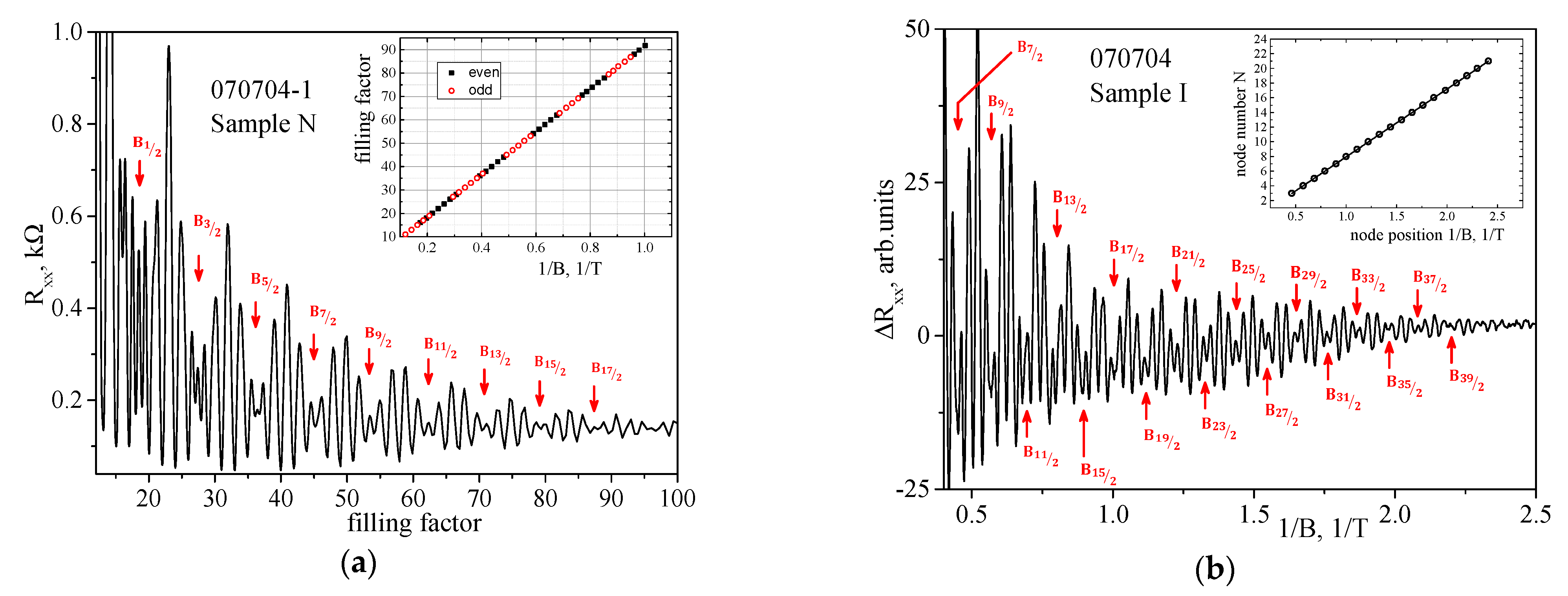
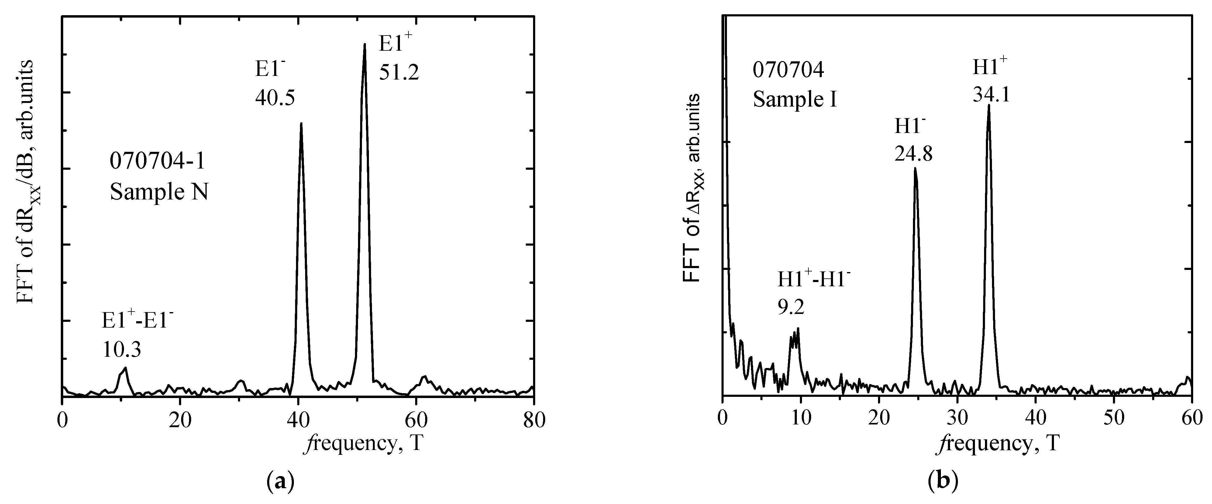
4.1. Fourier Analysis of Oscillations

One of the main methods of the frequency analysis of oscillations is the Fast Fourier Transform (FFT) of Rxx data to determine the characteristics of oscillations, such as frequency, phase and amplitude. For a detailed analysis of the SdH oscillations, we subtract the monotonous part of the Rxx(B) dependence. This can be carried out in two ways: by subtracting the polynomial, the degree of which is selected as the best centering of the oscillations along the x axis (see Figure 3b) or by numerical differentiation of the data. Both ways of processing were used and the results were compared, so the most pictorial presentation of the data is given in the paper. The results of the Fourier analysis of the Rxx(1/B) data for Sample N (Figure 3a) are shown in Figure 4a. It can be seen that only two close frequencies F are resolved, which correspond to the spin-orbit splitting of the E1 subband. In addition to the main peaks, designated E1+ and E1, there are other peaks that correspond to the combinations of frequencies from the main peaks. The sum of the densities obtained from the frequencies of peaks E1+ and E1 gives nFFT = 2.21 × 10¹⁶ m−2, (nFFT = e h F = e h (F+ + F)), which ideally corresponds to the data for this sample that were obtained from other regions of magnetic fields. The parameters of the samples under study are summarized in Table 2.
Figure 3b for Sample I shows the dependence of the oscillating part ΔRxx = RxxRmon with a residue of the monotonic part approximated by a polynomial, Rmon = m 1 / B m , on the reciprocal magnetic field 1/B. In Sample I, it can be seen that the oscillations are periodic in the reciprocal magnetic field and have pronounced beating nodes. However, for this sample, it was not possible to establish the correspondence of the positions of the oscillation minima to the integer values of the filling factor ν, since electrons with lower mobility participate in the conductivity (see discussion in Appendix A). The results of the Fourier analysis of the data ΔRxx(1/B) for Sample I (Figure 3b) are shown in Figure 4b. Again, only two close frequencies are resolved, which correspond to the spin-orbit splitting of the H1 subband. The sum of the densities obtained from the frequencies of peaks H1+ and H1 gives nFFT = 1.43 × 10¹⁶ m−2, which ideally corresponds to the data obtained from the low magnetic fields nHall (see Table 2). In addition to the main peaks, designated H1+ and H1, there are other peaks that correspond to combined frequencies. Thus, the low-frequency peak at f3 = 9.3 T is a difference peak from the main peaks H1+H1 = (34.1–24.8) T.
Winkler [31] showed that spin-splitting energy should be proportional to k||3 for a p-type state (heavy holes) Γ8 with Jz = ±3/2, but for an electron-like state of s-type Γ6, Jz = ±1/2, and a light hole state Γ8 with Jz = ±1/2, spin-splitting should be a linear function of wave number k||. Then, for p-type states with Jz = ±3/2 for the parameters of the Rashba spin-orbit splitting, we have:
ε Γ 8 S O = ± β E z k 3 ,   β E z = 2 2 m * X ( 2 X ) 4 π n ,   X = 2 ( 2 + 1 a 2 ) a 2 + 3 ,   a = Δ n n ,   Δ n = n + n ,   n = n + + n ,   Δ R Γ 8 = 2 β E z k F 3  
For the s-type states with Jz = ±1/2 the parameters of the Rashba spin-orbit splitting are given:
ε Γ 6 S O = ± α E z k ,   α E z = 2 m * π 2 Δ n n Δ n ,   Δ R Γ 6 = 2 α E z k F ,
where ε Γ 6 , 8 S O are the energies of spin-orbit splitting states with different symmetries, n and Δn are the sum and difference of electron densities in the aforementioned states, α, β are the spin-orbit interaction constants, and Ez is the effective electric field in the z direction.
Based on the difference in carrier densities in spin-split subbands, Δn, and knowing the effective mass of charge carriers, it is possible to determine the parameters of the Rashba spin-orbit interaction—the spin-orbit interaction constant, αEz and βEz, and the spin-orbit splitting energy at zero magnetic field, ΔR. The effective electron masses in the spin-split subbands of the studied structures were determined by the cyclotron resonance: Sample I, mc = 0.0376 m0, mc+ = 0.0417 m0 [25], and Sample N, mc = 0.0459 m0, mc+ = 0.0498 m0 [25]. To estimate the required parameters of the Rashba spin-orbit splitting in the samples under study, the average value of the effective mass m* ≈ 0.039 m0 (Sample I) и and m* ≈ 0.048 m0 (Sample N) can be used. Using the expression (1) for Sample I, we found βEz = 4.97 × 10⁻¹⁹ meV·cm3, ΔRΓ8 = 26.6 meV, and using the expression (2) for the Sample N, we obtained αEz = 37 × 10−12 eV·m, ΔRΓ6 = 27.4 meV (Table 2).

4.2. Analysis of the Beating Node Positions of SdH Oscillations in Magnetic Field

Let us use another way to determine the Rashba spin-splitting. In the quantum mechanical consideration, the occurrence of beatings of SdH oscillations is due to the presence of two types of energy splits in the spectrum (cyclotron and Zeeman) and the dependence of their ratio on the magnetic field. In our case, spin-orbit splitting in the zero field is also added. The specific SdH oscillation beating pattern observed in the experiment (Figure 3) is associated with the overlap of oscillations that are close in frequency from two spin-split subbands. Modulation of the amplitude of the SdH oscillations in this case is determined by cos(πδ/ℏωc); the beating nodes correspond to the points where cos amplitude is zero, which is the case when [32]
δ ω c   =   N + 1 2 ,   N = 0 ,   1 ,   2 , ,
where δ is the full spin-splitting,
δ ( B ) = Δ R + δ 1 ω c + δ 2 ( ω c ) 2 + .
The term quadratic in the field and higher-order terms become important in strong magnetic fields; in other cases, it is possible to restrict ourselves to the first two terms. The last beating node of SdH oscillations with increasing magnetic field is at δ/ℏωc =1/2. Thus, the field dependence of the total spin-splitting δ(B) can be obtained from the position in the magnetic field of the SdH oscillation beating nodes.
There are two ways to put numbers N for the beating nodes. Formula (3) leads to a simple recurrence relation for the position in the magnetic field of the beating nodes [33]:
B N + 1 2 / B N + 3 2 = ( N + 3 / 2 ) / ( N + 1 / 2 ) = ( 2 N + 3 ) / ( 2 N + 1 ) .
Thus, the positions in the magnetic fields in which the neighboring nodes are located refer to each other as the nearest odd numbers. If the experimental conditions make it possible to observe the beating nodes corresponding to small N, then using this procedure allows to the nodes to be unambiguously numerated.
Figure 3 shows the numbering of the beating nodes of the SdH oscillations in the studied samples using the recurrence relation (5). In Sample N, there are 14 nodes and the node with δ/ℏωc = 1/2 is visible. Sample I contains 19 nodes, with node δ/ℏωc = 7/2 corresponding to the largest magnetic fields. Thus, by knowing the numbers of the SdH oscillation beating nodes, one can obtain the field dependence of the total spin-splitting δ(B) (Figure 5; see discussion below).
The second method of node numbering is based on plotting the position of the beating nodes in a reciprocal magnetic field, 1/B, vs the node number, N (inset in Figure 3b). Expression (3) is rewritten in the following form
δ N ( B ) = ( N + 1 2 ) ω c = e m * B N ( N + 1 2 )
and, limiting only to the linear term in expression (4), we obtain
N + 1 2 = m * e Δ R 1 B i N + δ 1
which describes the plot in the inset to Figure 3b. The slope of the resulting straight line is determined by ΔR; therefore, the nodes can be numbered in an arbitrary way. The slope of the straight line does not depend on this. Correctly numbered nodes give the proper intercept on the y-axis. If the numbers of the SdH oscillation beating nodes are chosen correctly, then the free term of expression (7) makes it possible to determine the coefficient at the ℏωc.
The formula for the position of the beating nodes, which is analog of Equations (6)–(7) and allows for the parameters of the Rashba splitted band spectrum to be determined, was obtained in References [34,35].
The ΔR values obtained from the N(1/BN) plot (Figure 3) are as follows: 30.3 meV (Sample N) and 22.2 meV (Sample I), which is in good agreement with the values obtained using the Fourier analysis (Table 2).

4.3. Disscusion of Rashba Parameter Values

Let us analyze the results that were obtained for the Rashba spin-orbit splitting. It is worth noting that the constants of the Rashba SO interaction, α and β, are determined by the band structure parameters of the bulk semiconductor, namely [31,36,37]:
(α, β) ≈ Δ/|εg|.
Here, Δ = EΓ8EΓ7 is the spin-orbit splitting of the Γ8 and Γ7 bands in the crystal, εg = EΓ6EΓ8 is the energy gap between the Γ6 and Γ8 bands in crystals with narrow-gap (εg > 0) and gapless (εg < 0) semiconductors. According to (8), a strong Rashba spin-orbit coupling appears in 2D structures based on narrow-gap (CdHgTe) and gapless (HgTe) semiconductors, due to their small |εg|.
It should be noted that the ΔR values obtained in the present study for structures with different types of band structure are almost the same. This is apparently due to the large fraction of p-type wave functions in the E1 subband of Sample N (see the inset in Figure 1b [25]). For the states of the H1 subband of the Sample I, the contribution of the p-type states to the eight-component wave function reaches 50%; for the E1 subband of Sample N, this fraction is less, but close to 40%. Calculations give the spin-splittings at the Fermi level ΔRcalc = 21 (Sample I) and 17 (Sample N) meV [25], which is significantly less than the experimental results of this work.
In the pioneering work [11], the Rashba spin-splitting in HgTe SQW’s with an inverted band structure was investigated on the gate-controlled Hall devices. The QW’s were modulation doped symmetrically, on both sides of the HgTe QW, in one sample with a well width of 21 nm, and asymmetrically, only on the substrate side of the HgTe QW, in the other, with a well width of 12 nm, using CdI2 as a doping material. For the symmetrically doped case of (0.49–1.3) × 1012 cm−2 gate-control densities, the spin-orbit constant values changed from 8 × 10⁻¹⁹ meV·cm−3 to zero and then increased to 2 × 10⁻¹⁹ meV·cm−3. In the present work, with an asymmetric doped QW (Table 2), the density in the spin-splitted subbands, ns = 1.43 × 10¹⁶ m−2, exceeds the upper limit for density in Reference [11] and, correspondingly, the larger βEz parameter value was obtained.
The largest value of the Rashba spin-orbit splitting known in structures with rectangular HgTe QWs to date is 30 meV, observed in the 12.5-nm-wide HgTe/Hg0.3Cd0.7Te (001) QW with a density of 2.7 × 1012 cm−2 doped asymmetrically on the top barrier of the QW, using CdI2 as a doping material [12]. It was underlined that this large ΔR in HgTe QWs with an inverted band structure is caused by its narrow gap, the large spin-orbit gap between the bulk valence bands Γ8 and Γ7, and the heavy-hole character of the first conduction subband. The value of Reference [12] is quite close to the result of our work for Sample I with inverted band structures; thus, the same reasons for their large Rashba spin-splitting should be valid here.
The Rashba spin-splitting, as a function of carrier density, was investigated in a high-mobility 2DEG formed in p-type Hg0.77Cd0.23Te inversion layers with a normal band structure using WAL analysis [24]. The values of ΔR and α were 2–10 meV and 8–24 × 10−12 eV·m in the density range from 3 × 1011 cm−2 to 6 × 1011 cm−2. It was found that both ΔR and α, obtained from the experiment, were much smaller than the values predicted by the linear Rashba model. This discrepancy was explained by the nonlinear Rashba effect, which was caused by the weakening of interband coupling between the valence and conduction bands with increasing k. In our study, both ΔR and α were far larger than the known values [24], and this was associated with the different carrier densities in the compared samples.
The results for ΔR in HgTe-based QW’s are summarized in Figure 4 of Reference [15]. One can see that the ΔR values for structures with a normal band structure were within 10 meV, while the QW’s with inverted band structure had far larger values, of up to ~34 meV, which were obtained in two-dimensional electron gas confined in inversion layers on Hg1−xCdxTe with an inverted band structure (x = 0.10 − 0.09), with electron densities of 1.32 × 1012 cm−2 and 1.55 × 1012 cm−2 in two samples [15].

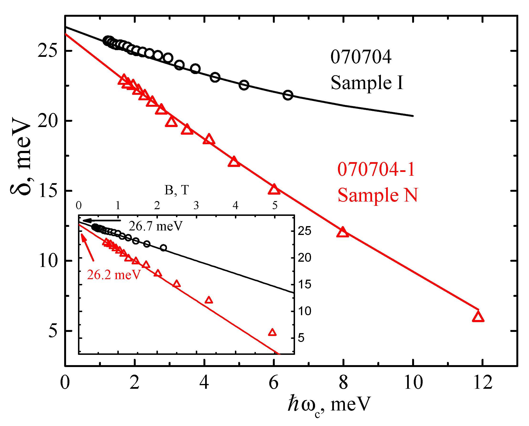
4.4. Magnetic Field Dependence of the Total Spin Splitting

In magnetic field B, the energy spectrum for the n-th Landau level may be presented, considering both the Zeeman spin splitting, Δ Z = g μ B , and the spin-orbit splitting of Rashba, ΔR, as [38]:
E 0 = 1 2 ω c   for   n = 0 , E n ± = ω c [ n ± 1 2 ( 1 g m * 2 m 0 ) 2 + n Δ R 2 E F ω c ] .  
Then, the total spin splitting, δ(B), is determined by the expression [38]:
δ ( B ) = [ ( ω c g μ B B ) 2 + Δ R 2 ] 1 / 2 ω c { Δ R ω c ,   if   ω c   Δ R 1 g m * 2 m 0   g m * 2 m 0 ω c ,   if   ω c   Δ R 1 g m * 2 m 0  
The result of Equation (10) can be understood in the following way [38]. In high magnetic fields, the spin-orbit-coupled states are strongly separated in energy, which significantly reduces the coupling effect, and the spin-splitting δ (Equation (10)) approaches the Zeeman splitting. In low magnetic fields, the spin-splitting δ (Equation (10)) linearly decreases with ω c ; the slope of this linear reduction is determined by the effective mass of charge carriers. In high magnetic fields, Zeeman splitting predominates, and this limit can be used to estimate the g-factor.
The theoretical model [38] was developed for the two spin-splitting mechanisms of Dresselhaus (BIA) and Rashba, and it was shown that only accounting for BIA or assuming that the BIA term has a comparable strength to the Rashba effect significantly deteriorated the agreement with the perpendicular-field experimental data. The key role of Rashba term was revealed, and the analytical expression Equation (10) was obtained.
The low field limit of Equation (10) is examined in the inset of Figure 5. For Sample N with a normal band structure, a deviation from linear dependence of δ ( B ) was observed at B > 1.5 T. For Sample I, the low field limit is well-described by the calculated values of δN in approximately the whole range of the magnetic field. The values of Δ R , obtained by approximating the dependence δ(B) to B → 0, coincide well with the values obtained from the Fourier analysis and the N(1/B) plot (see Table 2). In Figure 5, the spin-splitting, as a function of ω c , is presented for the two samples under study. It can be seen that a good description by theoretical Equation (10), with effective masses and g-factors as a fitting parameters, is observed for both QWs. The following parameters were obtained for the theoretical curves (solid lines in Figure 5): m c o r r * = 0.039 m 0 , | g | = 35 (Sample I) and m c o r r * = 0.024 m 0 , | g | = 30 (Sample N). An adequate description of the experimental data by the theoretical dependence (10) indicates the predominance of the Rashba contribution to the spin-orbit splitting at B = 0 than the contribution of Dresselhaus.
The importance of the experimental determination of the effective mass and g-factor in systems with a sophisticated dispersion law, to which the structures based on HgTe belong, is beyond doubt. The previously obtained experimental values of the g-factor and effective mass for HgTe quantum wells are contradictory and depend on the width of the quantum well and the electron density [39,40,41,42,43,44,45,46]. It was previously noted [39,40,41,42] that there is a problem of accordance between theoretical and experimental estimates of the effective mass in such QWs. If we systematize the currently available numerous experimental estimates of the effective mass in QWs based on HgTe, it is shown that with an increase in the density of charge carriers from ~2 × 10¹⁵ m−2 to ~1 × 10¹⁶ m−2  m * / m 0 increases from ~0.020 to (0.026–0.034) (see, for example, [42,43,44,46]). In the structures with a normal spectrum, the experimental values of the effective mass are close those calculated by the kP method over the whole density range; with the increasing QW width, in an inverted spectrum regime, the experimental values of effective mass become noticeably smaller than the calculated ones [42]. The values of m * / m 0 and g-factors obtained by fitting δ(B) dependence with Equation (10) are in good accordance with the previously obtained results for HgTe QWs.

5. Conclusions

Studies were carried out on quantum magnetotransport in heterostructures based on CdHgTe solid solutions, with a varying Cd (Hg) content in both the quantum well and the barriers. It is possible to realize systems with both normal and inverted energy spectra by compositional variations in quantum wells with a similar width.
We used several methods to estimate the Rashba spin-splitting, and then compared the results. Estimations for both the normal and inverted band spectra were made: from the difference in the carrier concentration in the spin-split subbands found by the Fourier analysis of SdH oscillations and from the analysis of the beating node positions of SdH oscillations in both low magnetic fields and the wider range of magnetic fields. Parameter estimates using different methods were in good agreement with each other.
Due to the high quality of the samples and the high concentration of electrons (n > 1.4 × 1012 cm−2), a remarkably rich SdH oscillation pattern is observed in our structures: high-resolution oscillations with well-defined beating nodes for numbers from N = 0 ( δ / ω C = 1 / 2 ) up to N = 14 and N = 19 in QWs with the normal and inverted energy spectra, respectively.
This allowed to describe the experimental data for the total spin-splitting, δ (B), in a wide range of magnetic fields using a theoretical expression, considering both Zeeman and Rashba effects with the effective mass values and the g-factor as the fitting parameters. The very fact of the adequate description of the data obtained using this theoretical dependence indicates the predominant Rashba contribution to the spin-orbit splitting at B = 0 in comparison with the contribution of Dresselhaus.
We note that the large Rashba splitting at B = 0 obtained in the present study for structures with different types of band structure is almost the same (ΔR ~ 25 ÷ 27 meV), due to the significant fraction of p-type wave functions in both the E1 subband of the 070704-1 structure and the H1 subband of the 070704 structure.

Author Contributions

S.V.G.: conceptualization, methodology, investigation, formal analysis, visualization, writing—original draft preparation, writing—review and editing, project administration. V.N.N.: methodology, investigation, formal analysis, software. validation. M.R.P.: formal analysis, visualization, resources. K.V.T.: investigation, software. S.M.P.: resources, investigation. N.G.S.: conceptualization, methodology, writing—review and editing, validation. M.V.Y.: writing—review and editing, funding acquisition, validation. N.N.M.: resources. S.A.D.: resources. All authors have read and agreed to the published version of the manuscript.

Funding

This research was funded by the Ministry of Science and Higher Education of the Russian Federation, grant 075-15-2020-797 (13.1902.21.0024).

Data Availability Statement

The data that support the findings of this study are available from the corresponding author upon reasonable request.

Acknowledgments

Experiments were carried out at the Collaborative Access Center “Testing Center of Nanotechnology and Advanced Materials” of the M.N. Mikheev Institute of Metal Physics of the Ural Branch of the Russian Academy of Sciences. The authors are very grateful to V.Ya. Aleshkin for program of band structure calculation.

Conflicts of Interest

The authors declare no conflict of interest. The funders had no role in the design of the study; in the collection, analyses, or interpretation of data; in the writing of the manuscript, or in the decision to publish the results.

Appendix A

As mentioned previously, two types of carriers, with significantly different mobilities, participated in the conduction for Sample I, as was concluded from the shape of the ρxx(B) and ρxy(B) curves, and from the difference in the electron densities determined from the range of classical magnetic fields, SdH oscillations and QHE regime. Let us discuss this fact in detail. When several types of charge carriers take part in the transport phenomena, each of them makes an additive contribution to the conductivity tensor:
R H = σ x y / B σ x x 2 + σ x y 2 ,   ρ x x = σ x x σ x x 2 + σ x y 2 σ x x = k e k n k μ k 1 + μ k 2 B 2 ,   σ x y = k e k n k μ k μ k B 1 + μ k 2 B 2
where R H —Hall constant, k—summation index over the number of types of charge carriers. Hence, the expressions for RH(B) and ρxx(B) follow, and are used in the analysis of positive magnetoresistance and the Hall effect for presence of two types of electrons [21]:
R H = n 1 μ 1 2 + n 2 μ 2 2 + μ 1 2 μ 2 2 B 2 ( n 1 + n 2 ) e [ ( n 1 μ 1 + n 2 μ 2 ) 2 + μ 1 2 μ 2 2 B 2 ( n 1 + n 2 ) 2 ,   ρ x x = n 1 μ 1 + n 2 μ 2 + μ 1 μ 2 B 2 ( n 1 μ 1 + n 2 μ 2 ) e [ ( n 1 μ 1 + n 2 μ 2 ) 2 + μ 1 2 μ 2 2 B 2 ( n 1 + n 2 ) 2
where n1, n2, μ1, μ2—densities and mobilities of electrons of the first and second types.
Dependences ρxx(B) with a smoothed oscillating part and RH(B) for Sample I are shown in Figure A1a. The RH(B) curve has a characteristic form for the conduction of two types of electrons with significantly different mobilities, as evidenced by two regions of RH(B) flattening at B < 1 T and B > 5 T. A small beak on the RH(B) curve at B < 0.2 T corresponds to the difference in the mobility of electrons from the spin-orbitally split sub-bands of the H1 level. Let us describe the dependencies ρxx(B) and RH(B) by expressions (A2), with the density and mobility of electrons of the first and second types n1, n2, μ1, μ2 used as the fitting parameters. The index k = 1 denotes the parameters of electrons of the spin-orbit split level H1, n1 = n + + n , μ1 = μ e f f , where the value of effective mobility, μ e f f , can be roughly estimated from the relation μ e f f     n + n 1 μ + + n n 1 μ . The index k = 2 denotes the density and mobility of low-mobility electrons.
Figure A1. (a) Dependences of the monotonous part of ρxx and Hall constant, RH, on magnetic field B (solid lines) for Sample I and their fitting by Equation (A2) (dash lines). The resulting fitting procedure parameters are also displayed. (b) Dependences of σxx (solid lines) and σxy (dash lines) on magnetic field B for the low-mobility and high-mobility (inset) electrons, plotted with Equation (A1) using parameters from fitting procedure (Figure A1a).
Nanomaterials 12 01238 g0a1
The fitting results are shown in Figure A1a by the dashed lines. It can be seen that the fitting curves describe the experimental data quite well. The obtained parameters are n1 = 1.40 × 10¹² m−2, μ1 = 24.5 m2/V × s; n2 = 3.20 × 10¹² m−2, μ2 = 0.13 m2/V·s. First, it should be noted that n1 is in excellent agreement with the nHall and the nFFT (Sample I). Second, the total density of electrons of the first and second types, obtained from the fit n = n1 + n2 = (1.40 + 3.20) × 1012 m−2 = 4.60 × 10¹² m−2, is in good agreement with the data from the QHE nQHE = 4.30 × 10¹² m−2. Third, we can observe a huge mobility ratio μ1/μ2 = 24.5/0.13~200, which indicates that we are dealing with conductivity not in the second size-quantized subband, but parallel conductivity in the doped layer in the barrier. This assumption is also supported by the fact that the quantum well in Sample I is rather shallow in terms of the ratio of Cd content in the barriers and in the well of 0.6/0.05/0.53 (see Table 1) as compared with the classical structure 0.7/0/0.7 and with Sample N 0.89/0.15/0.85. Let us make a simple estimate of the two-dimensional carrier density in the doped layer: nimp2D = nimp × dimp = 1.8 × 10¹⁸ [cm−3] × 13.5 × 10−7 [cm] = 4.05 × 10¹² [cm−2], nimp2Dn1 = (4.05 − 1.40) × 1012 = 2.65 × 10¹² [cm−2]. nimp2D is in fairly good agreement with the estimate of the carrier density from the QHE nQHE, and nimp2Dn1 is close to the value of n2 estimated from the fit (Figure A1a), which also confirms our assumption of parallel conductivity via the doped layer in the barrier.
Figure A1b shows the dependences of σxx and σxy on the magnetic field separately for the first and second types of electron—low-mobility (Figure A1b) and high-mobility electrons (inset in Figure A1b). It can be seen that the point σxx = σxy (Figure A1b), where ωcτ = μB = 1, separating the region of low classical and quantizing magnetic fields, is in a magnetic field of 7.8 T; therefore, the low-mobility electrons really not contribute to the SdH oscillation picture.

References

  1. Bychkov, Y.A.; Rashba, E.I. Oscillatory effects and the magnetic susceptibility of carriers in inversion layers. J. Phys. C Solid State Phys. 1984, 17, 6039–6045. [Google Scholar] [CrossRef]
  2. Bychkov, Y.A.; Rashba, E.I. Properties of a 2D electron gas with lifted spectral degeneracy. Pis’ma Zh. Eksp. Teor. Fiz. 1984, 39, 78–81. [Google Scholar]
  3. Vasko, F.T.; Prima, N.A. Spin splitting of spectrum of 2-dimentional electrons. Fizika Tverdogo Tela 1979, 21, 1734–1738. [Google Scholar]
  4. Sherman, E.Y. Random spin-orbit coupling and spin relaxation in symmetric quantum wells. Appl. Phys. Lett. 2003, 82, 209–211. [Google Scholar] [CrossRef] [Green Version]
  5. Dresselhaus, G. Spin-Orbit Coupling Effects in Zinc Blende Structures. Phys. Rev. 1955, 100, 580–586. [Google Scholar] [CrossRef]
  6. D’yakonov, M.I.; Kachorovskii, V.Y. Spin relaxation of two-dimensional electrons in noncentrosymmetric semiconductors. Sov. Phys. Semicond. USSR 1986, 20, 110–112. [Google Scholar]
  7. Zawadzki, W.; Pfeffer, P. Spin splitting of subband energies due to inversion asymmetry in semiconductor heterostructures. Semicond. Sci. Technol. 2004, 19, R1–R17. [Google Scholar] [CrossRef]
  8. Ivchenko, E.L.; Kaminski, A.Y.; Rössler, U. Heavy-light hole mixing at zinc-blende (001) interfaces under normal incidence. Phys. Rev. B 1996, 54, 5852–5859. [Google Scholar] [CrossRef] [PubMed]
  9. Nestoklon, M.O.; Golub, L.E.; Vchenko, E.L. Spin and valley-orbit splittings in SiGe∕Si heterostructures. Phys. Rev. B 2006, 73, 235334–235340. [Google Scholar] [CrossRef] [Green Version]
  10. Tarasenko, S.A.; Durnev, M.V.; Nestoklon, M.O.; Ivchenko, E.L.; Luo, J.-W.; Zunger, A. Split Dirac cones in HgTe/CdTe quantum wells due to symmetry-enforced level anticrossing at interfaces. Phys. Rev. B 2015, 91, 81302–81306. [Google Scholar] [CrossRef] [Green Version]
  11. Zhang, X.C.; Pfeuffer-Jeschke, A.; Ortner, K.; Hock, V.; Buhmann, H.; Becker, C.R.; Landwehr, G. Rashba splitting in n-type modulation-doped HgTe quantum wells with an inverted band structure. Phys. Rev. B 2001, 63, 245305–245308. [Google Scholar] [CrossRef]
  12. Gui, Y.S.; Becker, C.R.; Dai, N.; Liu, J.; Qiu, Z.J.; Novik, E.G.; Schäfer, M.; Shu, X.Z.; Chu, J.H.; Buhmann, H.; et al. Giant spin-orbit splitting in a HgTe quantum well. Phys. Rev. B 2004, 70, 115328. [Google Scholar] [CrossRef] [Green Version]
  13. Hinz, J.; Buhmann, H.; Schäfer, M.; Hock, V.; Becker, C.R.; Molenkamp, L.W. Gate control of the giant Rashba effect in HgTe quantum wells. Semicond. Sci. Technol. 2006, 21, 501–506. [Google Scholar] [CrossRef]
  14. Spirin, K.E.; Ikonnikov, A.V.; Lastovkin, A.A.; Gavrilenko, V.I.; Dvoretskii, S.A.; Mikhailov, N.N. Spin splitting in HgTe/CdHgTe (013) quantum well heterostructures. JETP Lett. 2010, 92, 63–66. [Google Scholar] [CrossRef]
  15. Gao, K.H.; Yu, G.; Sun, Y.; Kang, T.; Chen, X.; Dai, N.; Chu, J. Large spin-orbit splitting in inversion layers on HgCdTe with an inverted band structure. EuroPhys. Lett. 2018, 124, 27006. [Google Scholar] [CrossRef]
  16. Minkov, G.M.; Aleshkin, V.Y.; Rut, O.E.; Sherstobitov, A.A.; Dvoretski, S.A.; Mikhailov, N.N.; Solovèv, V.A.; Chernov, M.Y.; Ivanov, S.V.; Germanenko, A.V. Magneto-intersubband oscillations in two-dimensional systems with an energy spectrum split due to spin-orbit interaction. Phys. Rev. B 2020, 101, 245303–245307. [Google Scholar] [CrossRef]
  17. Minkov, G.M.; Aleshkin, V.Y.; Rut, O.E.; Sherstobitov, A.A.; Germanenko, A.V.; Dvoretski, S.A.; Mikhailov, N.N. Spin-orbit splitting of the conduction band in HgTe quantum wells: Role of different mechanisms. Phys. E Low Dimens. Syst. Nanostruct. 2019, 110, 95–99. [Google Scholar] [CrossRef] [Green Version]
  18. Drichko, I.L.; Smirnov, I.Y.; Suslov, A.V.; Baldwin, K.W.; Pfeiffer, L.N.; West, K.W. Dresselhaus spin-orbit interaction in the p -AlGaAs/GaAs/AlGaAs structure with a square quantum well: Surface acoustic wave study. Phys. Rev. B 2021, 104, 155302–155306. [Google Scholar] [CrossRef]
  19. Igor, Z.; Fabian, J.; Sarma, S.D. Spintronics: Fundamentals and applications. Rev. Mod. Phys. 2004, 76, 323–410. [Google Scholar]
  20. Tsidilkovski, I.M. Electron Spectrum of Gapless Semiconductors; Springer: Berlin, Germany, 1997. [Google Scholar]
  21. Tsidilkovski, I.M.; Harus, G.I.; Shelushinina, N.G. Impurity states and electron transport in gapless semiconductors. Adv. Phys. 1985, 34, 43–174. [Google Scholar] [CrossRef]
  22. König, M.; Wiedmann, S.; Brüne, C.; Roth, A.; Buhmann, H.; Molenkamp, L.W.; Qi, X.-L.; Zhang, S.C. Quantum Spin Hall Insulator State in HgTe Quantum Wells. Science 2007, 318, 766–770. [Google Scholar] [CrossRef] [PubMed] [Green Version]
  23. Schultzy, M.; Heinrichsy, F.; Merkty, U.; Colinz, T.; Skauliz, T.; Løvold, S. Rashba spin splitting in a gated HgTe quantum well. Semicond. Sci. Technol. 1996, 11, 1168–1172. [Google Scholar] [CrossRef]
  24. Liu, X.Z.; Yu, G.; Wei, L.M.; Lin, T.; Xu, Y.G.; Yang, J.R.; Wei, Y.F.; Guo, S.L.; Chu, J.H.; Rowell, N.L.; et al. The nonlinear Rashba effect in Hg0.77Cd0.23Te inversion layers probed by weak antilocalization analysis. J. Appl. Phys. 2013, 113, 013704–013708. [Google Scholar] [CrossRef]
  25. Bovkun, L.S.; Maremyanin, K.V.; Ikonnikov, A.V.; Spirin, K.E.; Aleshkin, V.Y.; Potemski, M.; Piot, B.A.; Orlita, M.; Mikhailov, N.N.; Dvoretski, S.A.; et al. Magnetooptics of HgTe/CdTe Quantum Wells with Giant Rashba Splitting in Magnetic Fields up to 34 T. Semiconductors 2018, 52, 1386–1391. [Google Scholar] [CrossRef]
  26. Mikhailov, N.N.; Smirnov, R.N.; Dvoretsky, S.A.; Sidorov, Y.G.; Shvets, V.A.; Spesivtsev, E.V.; Rykhlitski, S.V. Growth of Hg1-xCdxTe nanostructures by molecular beam epitaxy with ellipsometric control. Int. J. Nanotechnol. 2006, 3, 120–130. [Google Scholar] [CrossRef]
  27. Dvoretsky, S.; Mikhailov, N.; Sidorov, Y.; Shvets, V.; Danilov, S.; Wittman, B.; Ganichev, S. Growth of HgTe Quantum Wells for IR to THz Detectors. J. Electron. Mater. 2010, 39, 918–923. [Google Scholar] [CrossRef]
  28. Varavin, V.S.; Dvoretsky, S.A.; Liberman, V.I.; Mikhailov, N.N.; Sidorov, Y.G. Molecular beam epitaxy of high quality Hg1-xCdxTe films with control of the composition distribution. J. Growth Cryst. 1996, 159, 1161–1166. [Google Scholar] [CrossRef]
  29. Kvon, Z.D.; Olshanetsky, E.B.; Mikhailov, N.N.; Kozlov, D.A. Two-dimensional electron systems in HgTe quantum wells. Low Temp. Phys. 2009, 35, 6–16. [Google Scholar] [CrossRef]
  30. Bernevig, B.A.; Hughes, T.L.; Zhang, S.C. Quantum Spin Hall Effect and Topological Phase Transition in HgTe Quantum Wells. Science 2006, 314, 1757–1761. [Google Scholar] [CrossRef] [Green Version]
  31. Winkler, R. Rashba spin splitting in two-dimensional electron and hole systems. Phys. Rev. B 2000, 62, 4245–4248. [Google Scholar] [CrossRef] [Green Version]
  32. Das, B.; Miller, D.C.; Datta, S.; Reifenberger, R.; Hong, W.P.; Bhattacharya, P.K.; Singh, J.; Jaffe, M. Evidence for spin splitting in InxGal-xAs/In0.52Al0.48As heterostructures as B→0. Phys. Rev. B 1989, 39, 1411–1414. [Google Scholar] [CrossRef]
  33. Teran, F.J.; Potemski, M.; Maude, D.K.; Andrearczyk, T.; Jaroszynski, J.; Karczewski, G. Pauli Paramagnetism and Landau Level Crossing in a Modulation Doped CdMnTe/CdMgTe Quantum Well. Phys. Rev. Lett. 2002, 88, 186803–186804. [Google Scholar] [CrossRef]
  34. Dorozhkin, S.I.; Olshanetski, E.B. Distinctive features of the Shubnikov-de Haas oscillations in 2D systems with strong spin-orbit coupling and holes at the Si(110) surface. JETP Lett. 1987, 46, 502–506. [Google Scholar]
  35. Dorozhkin, S.I. Determination of energy spectrum parameters for two-dimensional carriers from the quantum oscillation beating pattern. Phys. Rev. B 1990, 41, 3235–3237. [Google Scholar] [CrossRef] [PubMed]
  36. Engels, G.; Lange, J.; Schapers, T.; Luth, H. Experimental and theoretical approach to spin splitting in modulation-doped InxGa12xAs/InP quantum wells for B→0. Phys. Rev. B 1997, 55, R1958–R1961. [Google Scholar] [CrossRef]
  37. de Andrada e Silva, E.A.; la Rocca, G.C.; Bassani, F. Spin-orbit splitting of electronic states in semiconductor asymmetric quantum wells. Phys. Rev. B 1997, 55, 16293–16297. [Google Scholar] [CrossRef]
  38. Das, B.; Datta, S.; Reifenberger, R. Zero-field spin splitting in a two-dimensional electron gas. Phys.Rev. B 1990, 41, 8278–8287. [Google Scholar] [CrossRef] [PubMed]
  39. Gudina, S.V.; Bogolyubskii, A.S.; Neverov, V.N.; Shelushinina, N.G.; Yakunin, M.V. Electron effective mass and g-factor in wide HgTe quantum wells. Semiconductors 2018, 52, 1403–1409. [Google Scholar] [CrossRef]
  40. Neverov, V.N.; Bogolubskii, A.S.; Gudina, S.V.; Podgornykh, S.M.; Turutkin, K.V.; Popov, M.R.; Shelushinina, N.G.; Yakunin, M.V.; Mikhailov, N.N.; Dvoretsky, S.A. Effective Mass and g-Factor of Two-Dimentional HgTe Γ8-Band Electrons: Shubnikov-de Haas Oscillations. Semiconductors 2020, 54, 982–990. [Google Scholar] [CrossRef]
  41. Bogolubskii, A.S.; Gudina, S.V.; Neverov, V.N.; Turutkin, K.V.; Podgornykh, S.M.; Shelushinina, N.G.; Yakunin, M.V.; Mikhailov, N.N.; Dvoretsky, S.A. Quantum oscillations of magnetoresistance in HgCdTe/HgTe/HgCdTe heterostructures with inverted band spectrum. Phys. Solid States 2021, 63, 1983–1993. [Google Scholar]
  42. Minkov, G.M.; Aleshkin, V.Y.; Rut, O.E.; Sherstobitov, A.A.; Germanenko, A.V.; Dvoretski, S.A.; Mikhailov, N.N. Electron mass in a HgTe quantum well: Experiment versus theory. Phys. E 2020, 116, 113742–113748. [Google Scholar] [CrossRef]
  43. Pfeuffer-Jeschke, A.; Goschenhofer, F.; Cheng, S.J.; Latussek, V.; Gerschütz, J.; Becker, C.R.; Gerhardts, R.R.; Landwehr, G. Cyclotron masses of asymmetrically doped HgTe quantum wells. Phys. B 1998, 256–258, 486–489. [Google Scholar] [CrossRef]
  44. Bovkun, L.S.; Krishtopenko, S.S.; Zholudev, M.S.; Ikonnikov, A.V.; Spirin, K.E.; Dvoretsky, S.A.; Mikhailov, N.N.; Teppe, F.; Knap, W.; Gavrilenko, V.I. Exchange Enhancement of the Electron g-Factor in a Two-Dimensional Semimetal in HgTe Quantum Wells. Semiconductors 2015, 49, 1627–1633. [Google Scholar] [CrossRef]
  45. Minkov, G.M.; Aleshkin, V.Y.; Rut, O.E.; Sherstobitov, A.A.; Dvoretski, S.A.; Mikhailov, N.N.; Germanenko, A.V. Anisotropy of the in-plane g -factor of electrons in HgTe quantum wells. Phys. Rev. B 2020, 101, 85305–85309. [Google Scholar] [CrossRef] [Green Version]
  46. Kvon, Z.-D.; Danilov, S.N.; Mikhailov, N.N.; Dvoretsky, S.A.; Prettl, W.; Ganichev, S.D. Cyclotron resonance photoconductivity of a two-dimensional electron gas in HgTe quantum wells. Phys. E 2008, 40, 1885–1887. [Google Scholar] [CrossRef] [Green Version]
Figure 1. Energies of size-quantized subbands at k = 0 as a function of the Hg 1 t Cd t Te quantum well width for t = 0.15 (Sample N) (a) and t = 0.05 (Sample I) (b).
Nanomaterials 12 01238 g001
Figure 2. The dependencies of longitudinal, Rxx, (black line) and Hall, Rxy, (red bold line) resistivities on the magnetic field B at T = 1.8 K for Sample N (a) and Sample I (b). The QHE plateaus in Rxy are marked with the corresponding filling factors ν = 11, 13 for Sample N and ν = 22, 20 for Sample I. Insets in (a,b) show the effect of weak antilocalization in both samples.
Nanomaterials 12 01238 g002
Figure 3. The oscillating part of Rxx curves (shown on Figure 2) vs filling factor for Sample N (a) and 1/B for Sample I (b). Node positions are denoted by the arrows. The numbering of nodes is indicated near the arrows. Insets: (a) Dependence of the oscillation minima positions in 1/B on the filling factor ν for Sample N. Filled squares denote even numbers; open circles denote odd ones. (b) Dependence of oscillation node positions in 1/B on its numbers N for Sample I.
Nanomaterials 12 01238 g003
Figure 4. FFT spectra of SdH oscillations of Sample N (a) and Sample I (b). The Fourier peaks are labeled as E1+ and E1 for Sample N and H1+ and H1 for Sample I according to corresponding spin-split subbands. Differential peaks are denoted as well.
Nanomaterials 12 01238 g004
Figure 5. Total experimental spin-splitting energies δ for Sample N (triangles) and Sample I (circles) as a function of ω c . Lines are the fitting according to Equation (10). Inset shows the low field limit, ω c Δ R 1 g m * 2 m 0 , of Equation (10). The Rashba spin-orbit splitting energies at B = 0, ΔR, obtained by low field fitting are indicated by arrows.
Nanomaterials 12 01238 g005
Table 1. Structural parameters of the samples under study.
Layer Order070704-1 (Sample N) 070704 (Sample I)
Width, nmCd ContentWidth, nmCd Content
CdTe cap371401
Cd 1 y Hg y Te barrier320.8531.50.53
Hg 1 t Cd t Te QW130.15150.05
Cd 1 x Hg x Te spacer9.50.8911.50.6
In doped layer nimp = 1.8 × 1018 cm−3100.8913.50.6
Cd 1 x Hg x Te barrier50.895.50.6
CdTe buffer6000160001
ZnTe buffer30 30
GaAs (013) substrate4 × 105 4 × 10⁵
Table 2. Electron gas and Rashba spin-orbit parameters of the samples under study.
Parameter (Definition Method)070704-1
Sample N
070704
Sample I
nQHE (QHE)2.18 × 10¹⁶ m−24.30 × 10¹⁶ m−2
nHall (nHall = 1/(RH·e))2.20 × 1016 m−21.46 × 10¹⁶ m−2
nFFT (FFT)2.21 × 10¹⁶ m−21.43 × 10¹⁶ m−2
n (two types of electrons)n11.40 × 1016 m−2
n23.20 × 1016 m−2
n = n1 + n24.60 × 1016 m−2
μ 2.0   m / ( V · s)
μ (two types of electrons)μ1 24.5   m / ( V · s)
μ2 0.13   m / ( V · s)
ΔR (FFT) 27.4   meV 26.6   meV
ΔR (N(1/BN) plot) 30.3   meV 22.2   meV
Δ R   ( low   field   limit   of   Equation   ( 10 )   ω c Δ R 1 g m * 2 m 0 ) 26.2   meV 26.7   meV
ΔRcalc [25] 17   meV 21   meV
α (FFT) 37 × 10 12   eV · m
β (FFT) 4.97 × 10 19 meV · cm 3
m * / m 0 (Equation (10))0.0240.039
m c * / m 0 [25]0.0480.039
| g | (Equation (10))3035
Publisher’s Note: MDPI stays neutral with regard to jurisdictional claims in published maps and institutional affiliations.

