Article

Implementation of Ambipolar Polysilicon Thin-Film Transistors with Nickel Silicide Schottky Junctions by Low-Thermal-Budget Microwave Annealing

Department of Electronic Materials Engineering, Kwangwoon University, Seoul 01897, Korea
*
Author to whom correspondence should be addressed.
Nanomaterials 2022, 12(4), 628; https://doi.org/10.3390/nano12040628
Submission received: 14 January 2022 / Revised: 3 February 2022 / Accepted: 10 February 2022 / Published: 13 February 2022
(This article belongs to the Special Issue The Application of Microwave-Assisted Technology in Nanomaterials)

Abstract

:
In this study, the efficient fabrication of nickel silicide (NiSix) Schottky barrier thin-film transistors (SB-TFTs) via microwave annealing (MWA) technology is proposed, and complementary metal-oxide-semiconductor (CMOS) inverters are implemented in a simplified process using ambipolar transistor properties. To validate the efficacy of the NiSix formation process by MWA, NiSix is also prepared via the conventional rapid thermal annealing (RTA) process. The Rs of the MWA NiSix decreases with increasing microwave power, and becomes saturated at 600 W, thus showing lower resistance than the 500 °C RTA NiSix. Further, SB-diodes formed on n-type and p-type bulk silicon are found to have optimal rectification characteristics at 600 W microwave power, and exhibit superior characteristics to the RTA SB-diodes. Evaluation of the electrical properties of NiSix SB-TFTs on excimer-laser-annealed (ELA) poly-Si substrates indicates that the MWA NiSix junction exhibits better ambipolar operation and transistor performance, along with improved stability. Furthermore, CMOS inverters, constructed using the ambipolar SB-TFTs, exhibit better voltage transfer characteristics, voltage gains, and dynamic inverting behavior by incorporating the MWA NiSix source-and-drain (S/D) junctions. Therefore, MWA is an effective process for silicide formation, and ambipolar SB-TFTs using MWA NiSix junctions provide a promising future for CMOS technology.

1. Introduction

Metal silicides, i.e., compounds of metal and silicon (Si), have been widely employed as interconnecting and contact materials in complementary metal-oxide-semiconductor (CMOS) technology due to their low specific resistivity, low contact resistivity towards both types of Si, high thermal stability, good processibility, and excellent process compatibility with standard Si technology [1,2,3,4]. Transition-metal silicide-based Schottky barrier (SB) source-and-drain (S/D) junctions have aroused much interest in nanoscale metal-oxide-semiconductor field-effect transistors (MOSFETs) because the resistive–capacitive (RC) time delay must be reduced by minimizing both parasitic resistance and capacitance components, in order to meet the major requirement of speeding up electronic circuits [5,6,7]. In SB-MOSFETs, the S/D junction consists of silicide in place of conventional impurity-doped silicon, thus enabling lower parasitic series resistance and ultrashallow abrupt junction formation via a simpler process [7,8,9,10]. By contrast, the performance of conventional MOSFETs is determined by doping and activation techniques, which become increasingly difficult for ultra-short-channel devices. Nevertheless, the Ti silicides (TiSix) and Co silicides (CoSix) that are commonly used in CMOS fabrication have limitations in future, extremely scaled down, ultra-high-density CMOS electronic circuits. In the case of TiSix, the sheet resistance (Rs) increases as the line width decreases [11,12,13,14], while in the case of CoSix, junction spiking becomes an issue due to excessive Si consumption [12,15,16]. Meanwhile, Ni silicide (NiSix) is gaining attention in next-generation deep submicron CMOS devices due to its improved nanoscale performance, and is gradually replacing CoSix [17]. In particular, there are many advantages, such as low specific resistivity (10–15 μΩ cm) and formation temperature (typically 500 °C), decreased Si consumption (1.83 nm of Si per nanometer of Ni, yielding 2.21 nm of NiSix), and little deterioration in resistivity on narrow lines/gates [16,18,19,20,21,22]. In particular, NiSix materials are the standard metal contacts in the semiconductor industry for both NMOS and PMOS devices, and are regarded as midgap metals with Schottky barrier heights (SBHs) of 0.45–0.5 eV for holes, and 0.6–0.65 eV for electrons [23,24]. Therefore, when applied to the S/D metallic junctions for Schottky barrier thin-film transistors (SB-TFTs), NiSix is particularly favorable for obtaining ambipolar operating characteristics without n-type or p-type impurity doping. Consequently, these devices are able to behave as p-type or n-type MOSFETs simply by changing the polarity of the gate bias.
The traditional silicide formation process has generally involved conventional rapid thermal annealing (RTA) using a halogen lamp. However, because the process is typically performed in a vacuum, RTA has the disadvantages of high cost, relatively long processing time, and high thermal budget [25,26]. By contrast, microwave annealing (MWA) does not require a vacuum, is cheaper, and has higher energy-transfer efficiency and consumption, a shorter process time, and a lower thermal budget [27,28]. There are several studies of applying MWA with these advantages to the activation of ion-implanted dopants [29,30]. In addition, MWA can offer quicker volume heating than the RTA, because it interacts directly with individual atoms while inducing dipole rotation in the silicon substrates [31]. Therefore, MWA is employed herein to promote the silicide reaction between Ni and Si. To verify the efficiency of silicidation by MWA, conventional RTA is also applied to NiSix formation for comparison. The crystallinity and Rs values of the NiSix prepared via MWA at various microwave powers, and by RTA at 500 °C, are evaluated. In addition, NiSix SB-diodes are fabricated via MWA at various microwave powers, and their electrical characteristics are measured to determine the optimum fabrication conditions. These conditions are then used to fabricate ambipolar NiSix SB-TFTs, and their electrical characteristics and reliability are evaluated in comparison with identical devices prepared via RTA. Further, CMOS-like inverters are constructed using the MWA- or RTA-NiSix SB-TFTs, in order to evaluate their voltage transfer characteristics, voltage gains, and dynamic inversion operation.

2. Materials and Methods

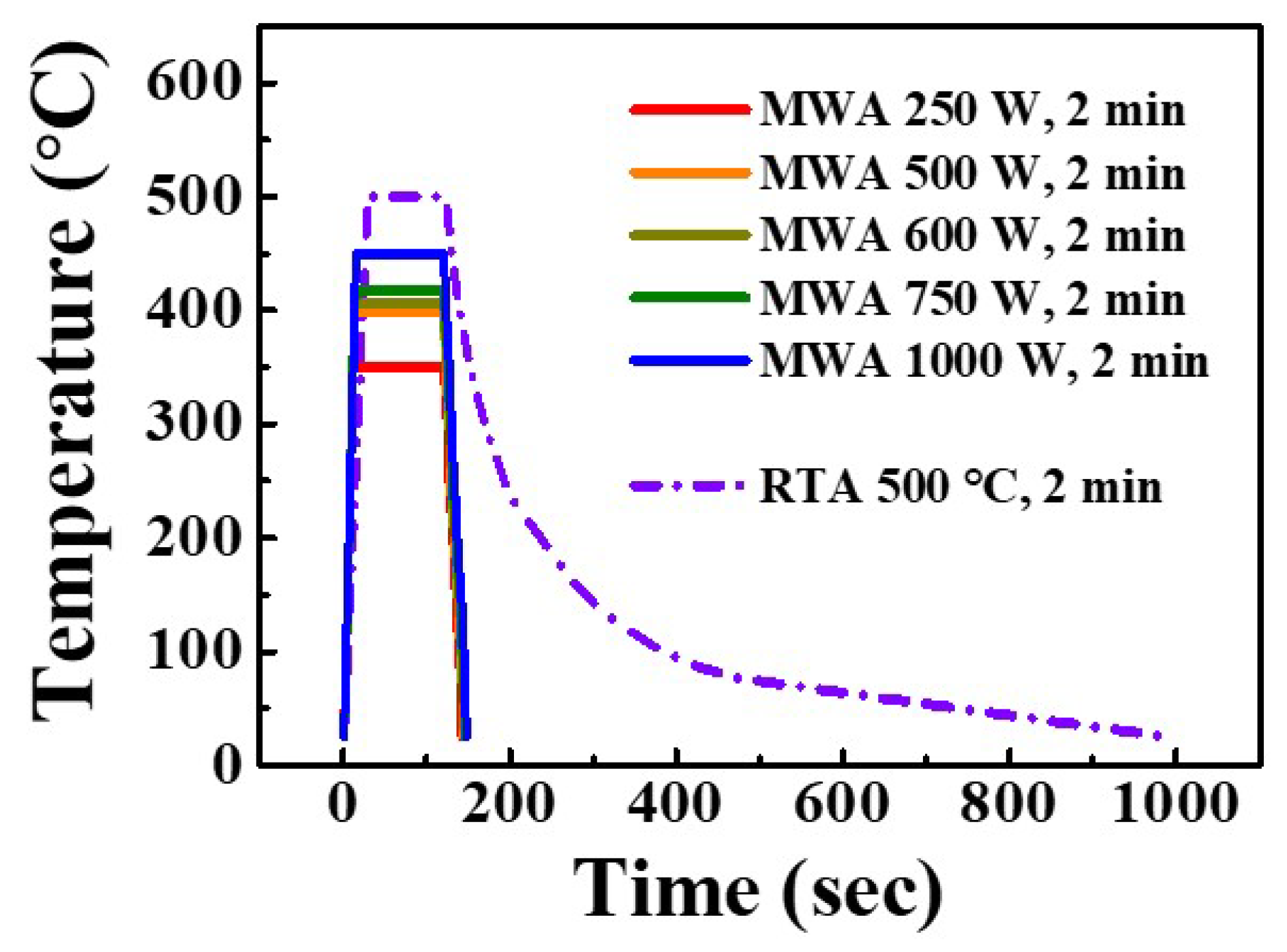
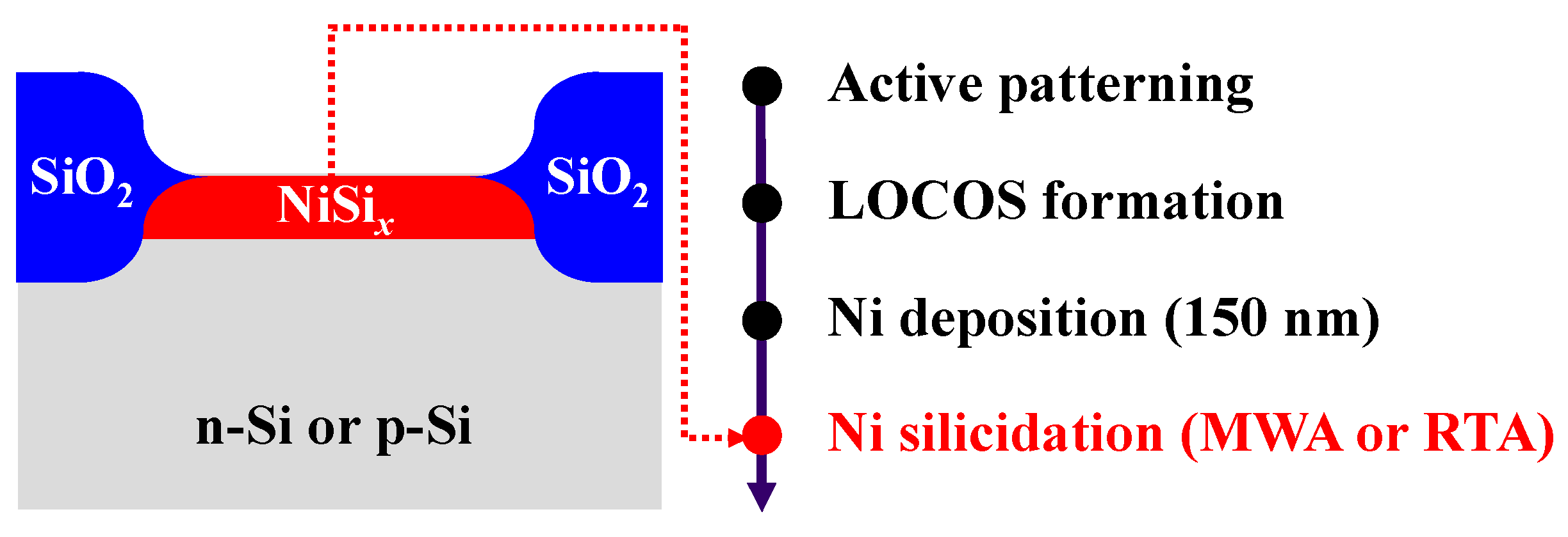
2.1. Nickel Deposition and Silicidation

The substrates were (100)-oriented n-type and p-type Si wafers with resistivities ranging from 10 to 20 Ω·cm. The substrates were cleaned using the process recommended by the Standard Radio Corporation of America (RCA) to remove any surface contamination and native oxides. Active regions were then formed via a photolithographic patterning process and wet etching with a 30:1 buffered oxide etchant (BOE). A 150 nm-thick Ni film was deposited using an electron-beam (E-beam) evaporator. After that, the MWA process was performed at powers of 250–1000 W under a N2 atmosphere for 2 min for NiSix formation. For comparison, the RTA process was conducted at 500 °C for 2 min under a N2 atmosphere. After that, the unreacted Ni was removed using a 1:1 sulfuric acid/hydrogen peroxide mixture (SPM) at room temperature.
The temperature profiles of the MWA and RTA processes are shown in Figure 1. We used an infrared (IR) thermometer to check the temperature during the MW treatment process, because it is hard to determine the temperature inside the MW chamber using metal thermocouples [32]. Thus, after heat treatment at 500 °C via the RTA process, about 15 min are required to return to room temperature, and the thermal budget is 2.84 × 10⁵ °C·s. By contrast, the MWA process is a volumetric heating method using electromagnetic waves, which reaches the process temperature within about 20 s and has a very short ramp downtime of 10 s. The thermal budget of the MWA process is 0.47 × 10⁵, 0.54 × 10⁵, 0.56 × 10⁵, 0.59 × 10⁵, and 0.65 × 10⁵ °C·s at operating powers of 250, 500, 600, 750, and 1000 W, respectively. This indicates that the MWA process generally has a lower thermal budget and a higher energy transfer efficiency than the RTA process.

2.2. Fabrication of the NiSix SB-Diodes

As shown schematically in Figure 2, phosphorus- and boron-doped (100) n-type and p-type bulk silicon wafers with resistivities of 3–5 and 7–14 Ω∙cm, respectively, were used to fabricate the NiSix-based SB-diodes. After defining the active area of the diode, a 500 nm-thick SiO2 layer was grown via wet oxidation at 980 °C for local oxidation of silicon (LOCOS) isolation. A 150 nm-thick Ni film was deposited using an E-beam evaporator. For NiSix formation, either the MWA process at a power of 250–1000 W for 2 min, or the RTA process at 500 °C for 2 min, was employed under a N2 atmosphere, to investigate the effect of MWA silicidation upon the characteristics of the SB-diodes. Then, unreacted Ni was removed using an SPM solution at room temperature.

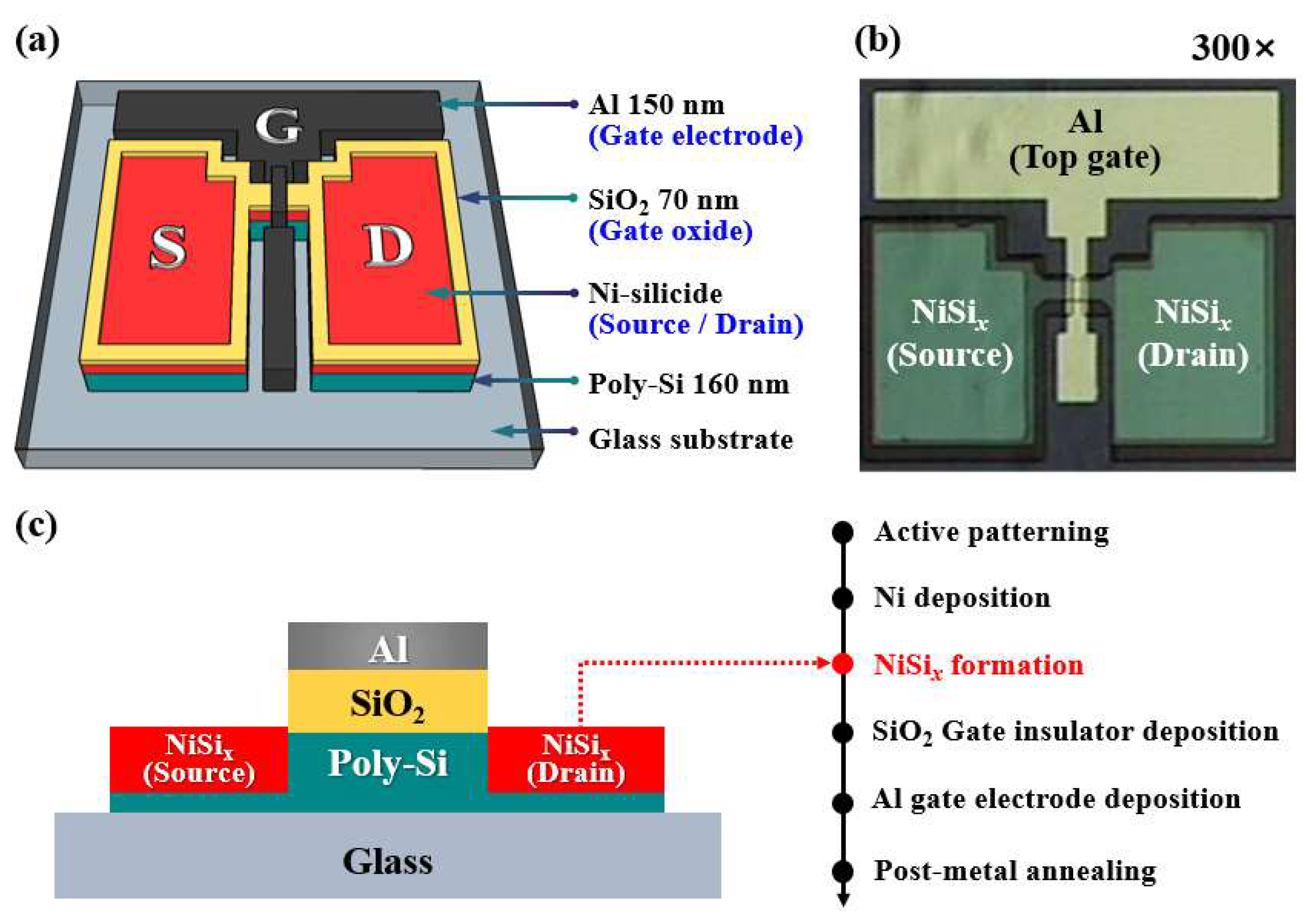
2.3. Fabrication of the NiSix SB-TFTs

Glass substrates (1737 and EAGLE2000TM, Corning) were each coated with a 160 nm-thick poly-Si layer via excimer-laser annealing (ELA) for use in fabricating the SB-TFTs with NiSix S/D junctions. The resulting ELA poly-Si substrate was then cleaned via the RCA process, after which the active channel regions were patterned via photolithography and wet etching with a 30:1 BOE solution. The channel width (W) and length (L) of the fabricated devices were 20 µm and 10 µm, respectively. Immediately after removing the native oxide film from the poly-Si channel with the 30:1 BOE, a 150 nm-thick Ni film was deposited using an E-beam evaporator. Subsequently, NiSix was selectively formed in the S/D region via the MWA process at 600 W, which is the optimal power condition. Then, unreacted Ni was removed using the SPM solution. For the gate insulator, a 70 nm-thick SiO2 film was deposited by radio-frequency (RF) magnetron sputtering at an operating pressure of 3.0 mTorr, an Ar flow rate of 30 sccm, an O2 flow rate of 2 sccm, and an RF power of 200 W. For the top-gate electrode, a 150 nm-thick Al film was deposited using an E-beam evaporator, then patterned by a lift-off method. Finally, post-metallization annealing (PMA) was performed using forming gas (5% H2, 95% N2) in a furnace at 400 °C for 30 min to improve the electrical properties. The schematic structure, process flow, and top-view optical microscope image (300×) of the fabricated NiSix SB-TFTs are presented in Figure 3.

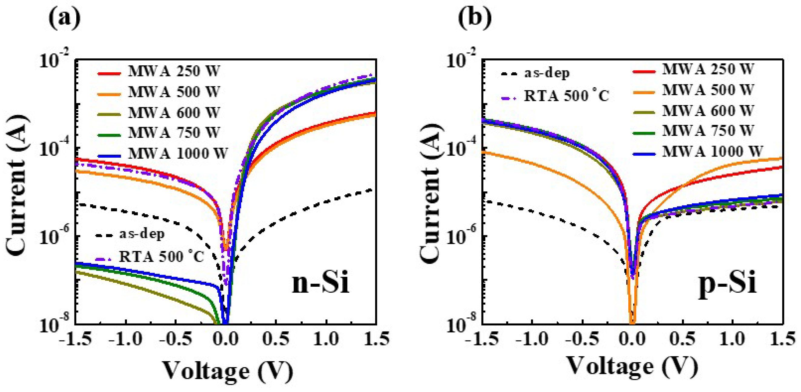
2.4. Characterization of the NiSix SB-Diodes and SB-TFTs

The electrical characteristics of the fabricated NiSix Schottky junction diodes and the SB-TFTs were measured using an Agilent 4156B precision semiconductor parameter analyzer in a dark box to prevent external effects such as light and electrical noise. In addition, CMOS inverters were constructed using the MWA- and RTA-processed NiSix SB-TFTs, and their voltage transfer characteristics, voltage gains, and dynamic inversion behaviors were evaluated using an RIGOL DG972 function/arbitrary waveform generator and RIGOL MSO5074 oscilloscope in a dark box.

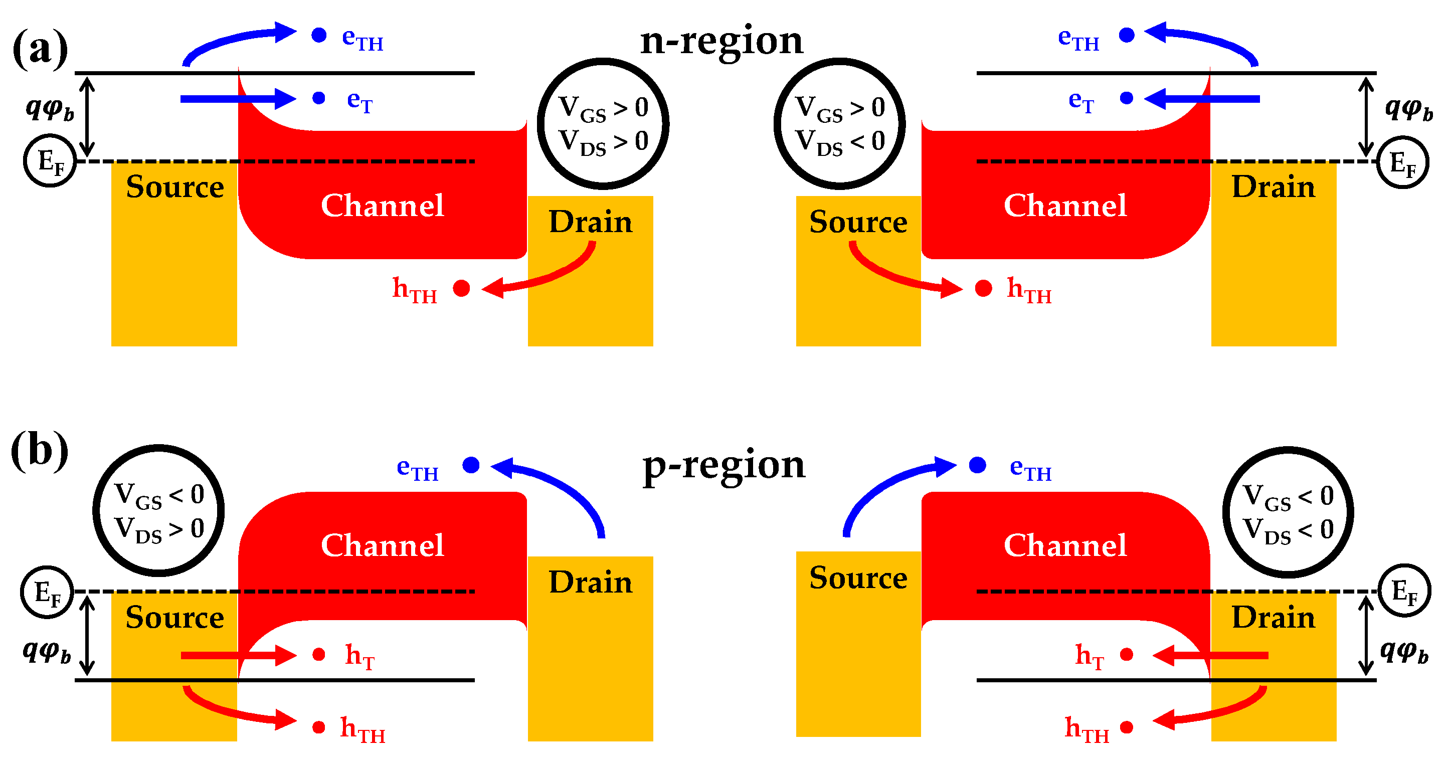
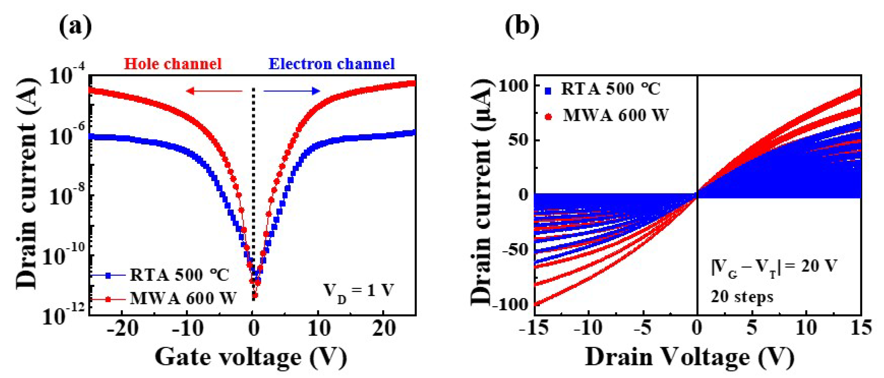
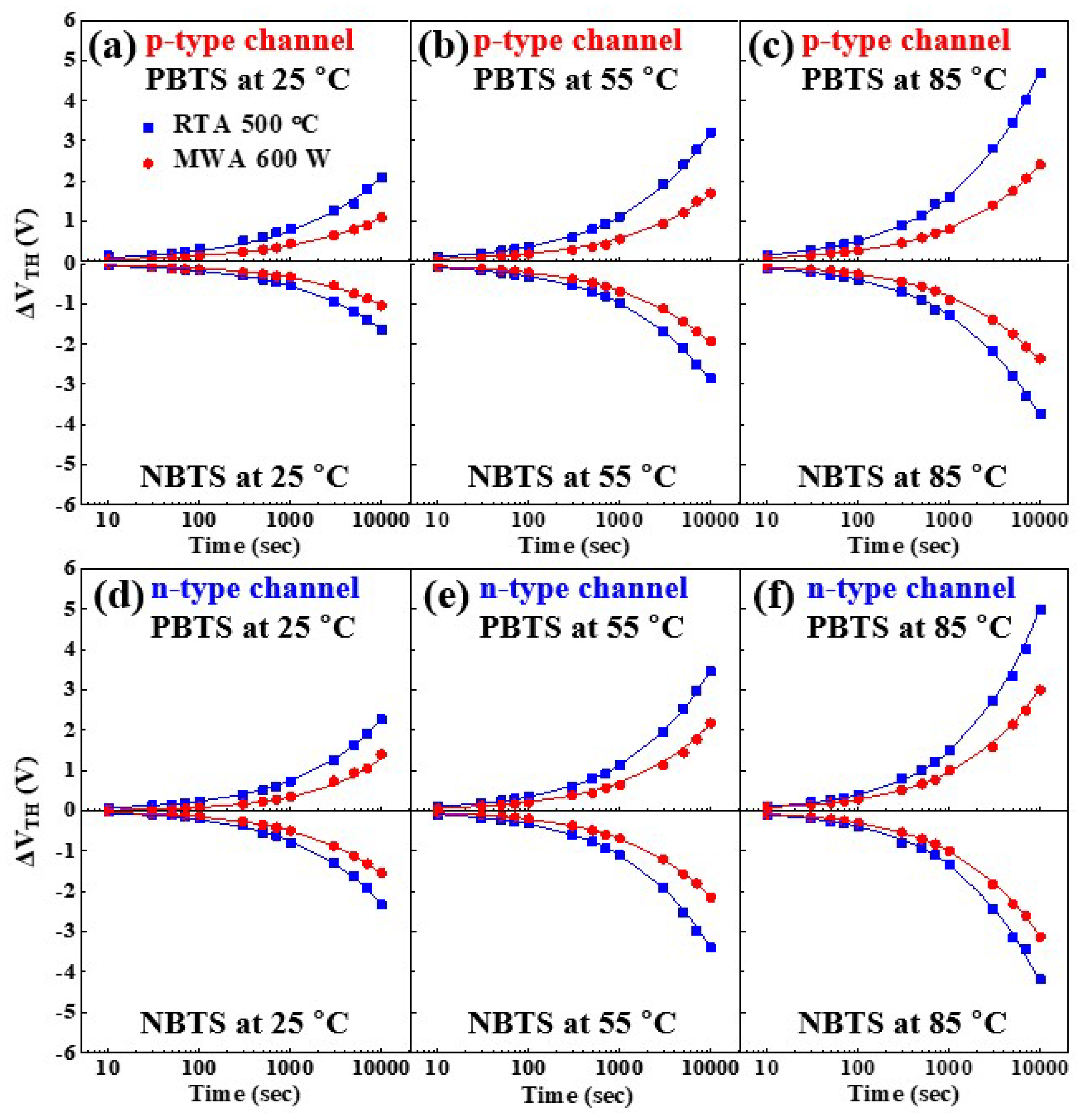
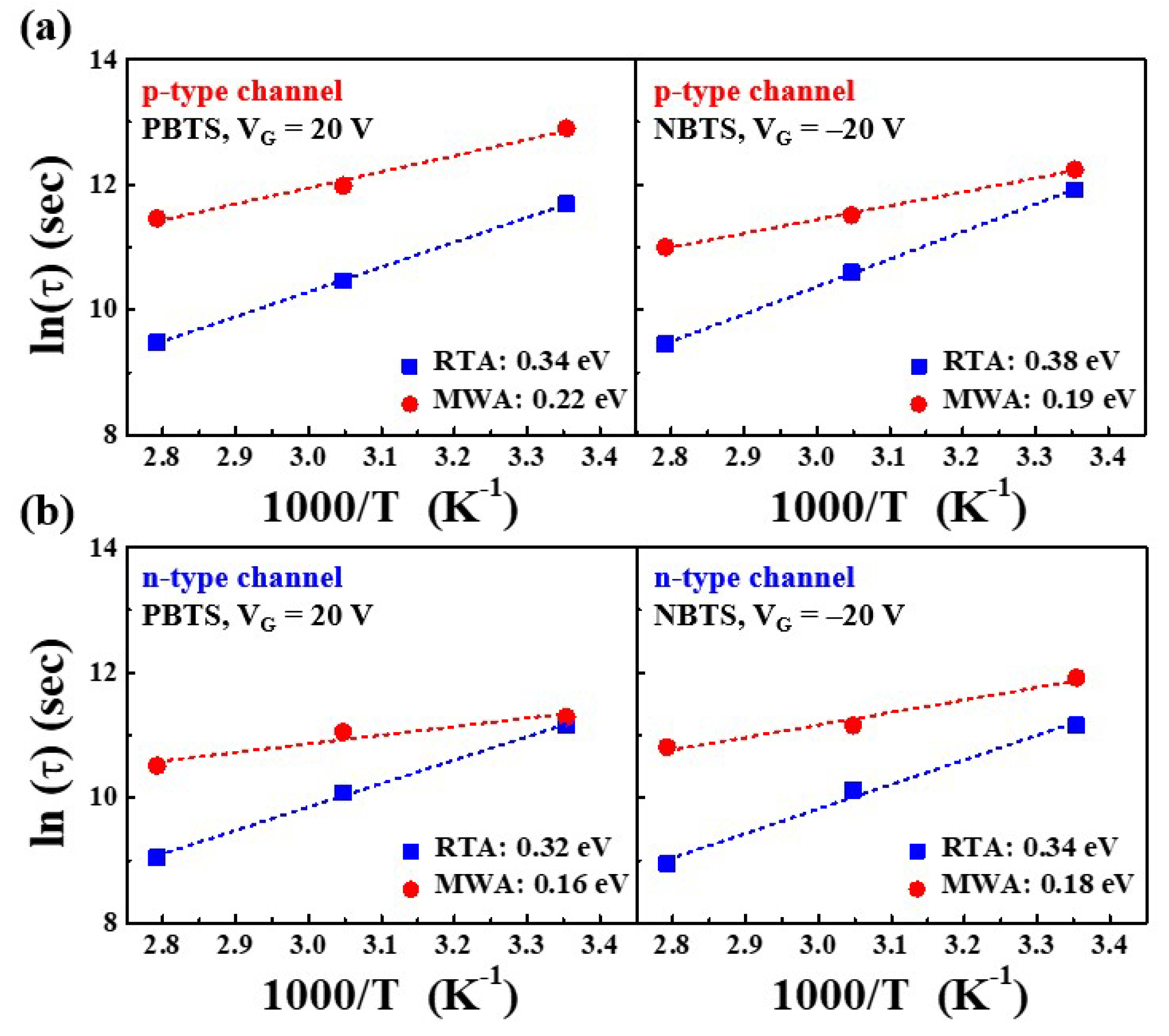
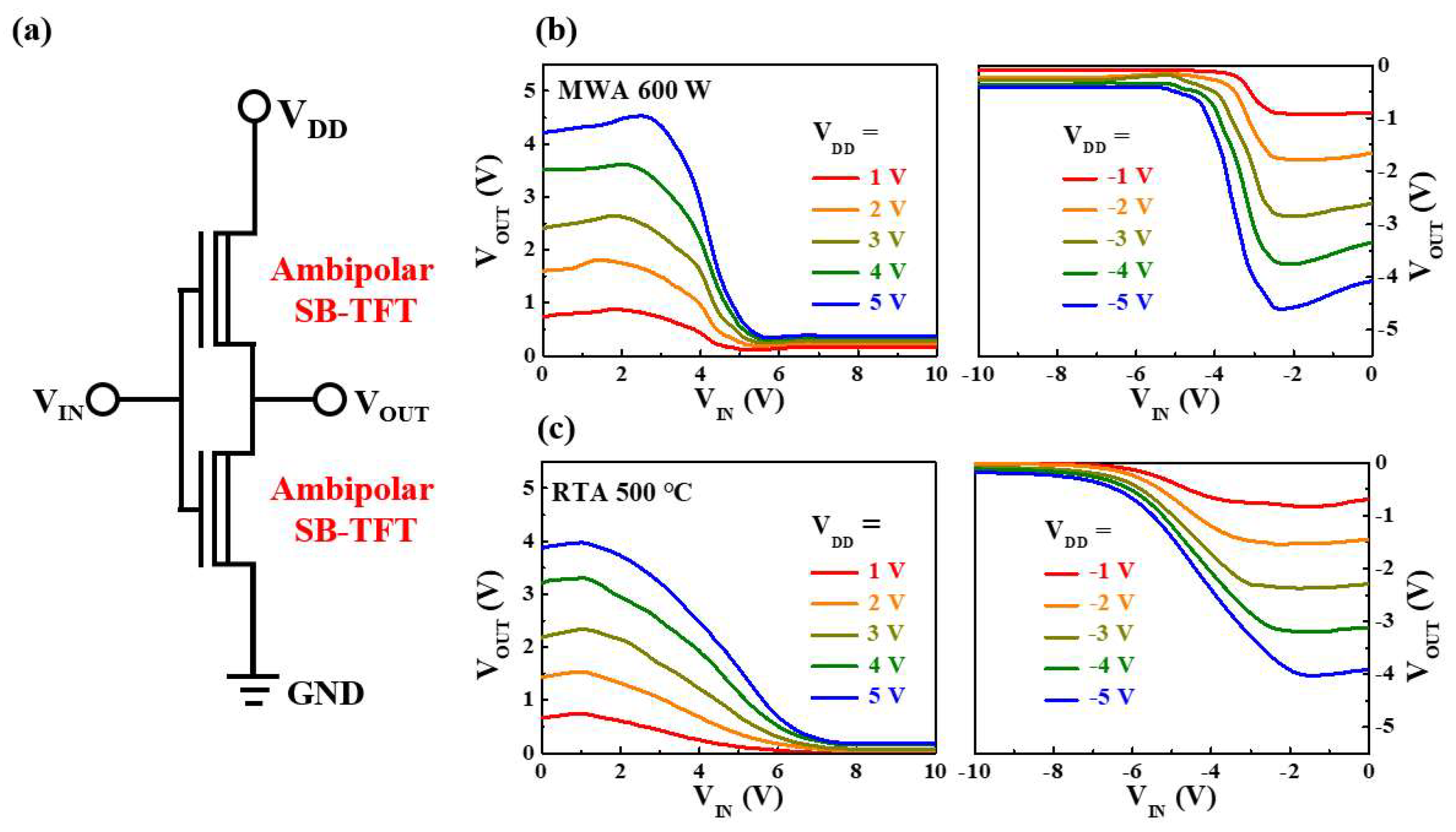
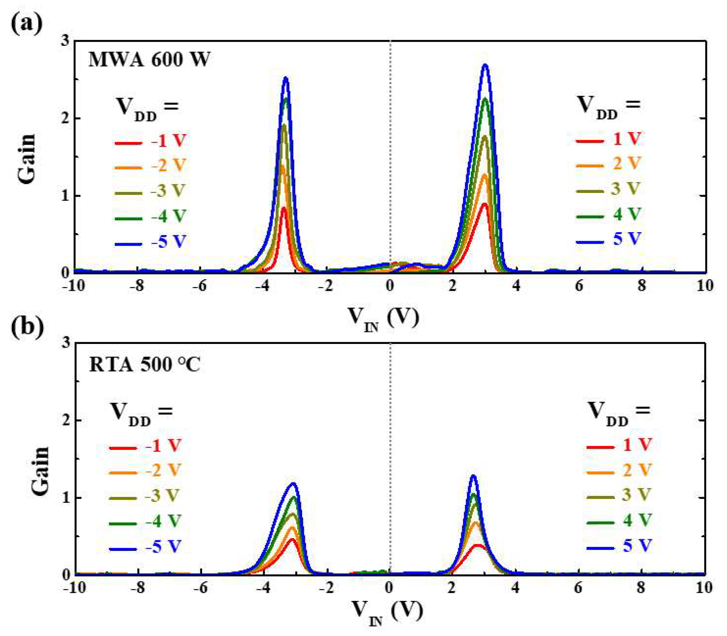
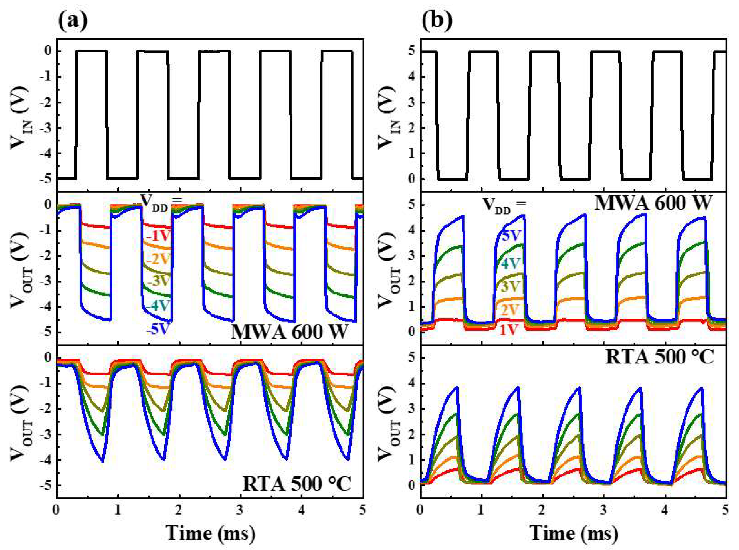
3. Results and Discussion

The sheet resistances (Rs) of the NiSix samples fabricated at various microwave powers were measured using a four-point probe, and the results are presented in Figure 4a. Here, a significant decrease in Rs is observed at 500 W, thus resulting in low resistance. In particular, the silicidation process at 600 W provides the lowest Rs value of 3.86 Ω/sq, which is lower than the 6.62 Ω/sq obtained via the RTA process at 500 °C. These results are similar to those reported in other literature [33]. Therefore, it is concluded that efficient silicide formation is possible even with a low-power MWA process, by sufficiently reducing the resistance.
The crystallinities of the various NiSix samples are indicated by the XRD spectra in Figure 4b. Here, the XRD pattern of the as-deposited Ni film exhibits peaks corresponding to the (111) and (200) crystal planes of Ni, while various other peaks appear after the RTA and MWA silicidation processes. In particular, the MWA treatment leads to the appearance of a peak corresponding to the (310) crystal plane of NiSix, even at a low microwave power of 250 W, thus confirming the formation of silicide. When the MWA process is performed at 500 W, several strong peaks corresponding to the (211), (220), (310), (221), and (301) crystal planes also appear [34], giving almost the same pattern as that obtained using the 500 °C RTA process. These results indicate that 600 W is the optimal MWA silicidation condition.
The current–voltage (I-V) characteristics of the NiSix Schottky junction diodes on n-type and p-type Si substrates according to the various silicidation conditions are presented in Figure 5a and Figure 5b, respectively, and the corresponding electrical parameters are summarized in Table 1. The as-deposited Ni SB-diode has a low on-current and a high leakage current due to interfacial defects between the unreacted Ni film and Si. However, as silicidation proceeds, the rectification characteristics of the n-type and p-type diodes are improved, and the on/off current ratio increases. In particular, the MWA process improves the operating performance as the microwave power increases, and exhibits the best rectification characteristics at 600 W. Notably, the 600-W MWA SB-diodes on the n-type substrate provide better results than the 500 °C RTA diodes. This is also evidenced by the ideality factors (η) extracted from the I-V curves, and the Schottky barrier heights (ϕb) extracted from the current–voltage (I-V) curves (Table 1); moreover, it is consistent with the Rs and XRD results. In addition, the ϕb values were extracted by Equation (1) [35]:
ϕ b ( V ) = ϕ b 0 + ( n 1 n ) V
where V, n are voltage and ideality factor, respectively.
Figure 6 shows schematic energy band diagrams based on VGS and VDS values for ambipolar operation. The current device is mainly related to thermionic emission and tunneling of carriers above the threshold in the SB-TFTs. The electrons are injected into the channel using thermionic emission (eTH) and tunneling (eT) from the source-and-drain electrodes at the positive and negative VDS, when the gate bias is positive (n-channel operation), as shown in Figure 6a. In Figure 6b, the holes are injected into the channel region by thermionic emission (hTH) and tunneling (hT) at the negative gate bias (p-channel operation). Depending on the operating mode, electrodes or holes from source-and-drain electrodes fill the channel region during the ambipolar operation. As a result, the driving current and Ion/Ioff of p-channel operation can be lower, because the SB height (SBH) for electrons in NiSix is slightly higher than the SBH for holes, but the effective electron mass of tunneling is lower.
The electrical properties of the NiSix SB-TFTs fabricated via the MWA silicidation process at 600 W, and via the RTA process at 500 °C, are presented in Figure 7. The transfer curves measured at a drain voltage (VD) of 1 V and a gate voltage (VG) range of −25 to +25 V (Figure 7a) demonstrate the ambipolar conduction properties of both devices. Meanwhile, the output curves measured at |VGVTH| = 0–20 V (where VTH is the threshold voltage) in the drain voltage range of −15 to +15 V demonstrate that both devices can behave as p-type (hole channel) or n-type (electron channel) MOSFETs simply by changing the polarity of the gate bias. The drain current (ID) increases linearly in the low VD region, indicating a pinch-off characteristic that gradually reaches the saturation region as VD increases further. Taken together, these results indicate that the 600-W MWA NiSix SB-TFT allows better switching characteristics and higher drive current than the 500-°C RTA-processed device. This is also consistent with the results obtained for the SB-diode.
The extracted electrical parameters of the 600-W MWA and the 500-°C RTA NiSix SB-TFTs are summarized in Table 2. The subthreshold swing (SS) and field-effect mobility (μFE) values were extracted using Equations (2) and (3) [36]:
S S = [ ( d l o g I D d V G ) ] 1
and
μ F E = ( L g m W · C o x · V D ,   g m = I D V G )
where L, W, gm, and Cox are the channel length, width, transconductance, and gate oxide capacitance per unit area, respectively. Thus, the 600-W MWA NiSix SB-TFT exhibits an SS of 633.4 mV/dec, a μFE of 16.5 cm2/V·s, and a VTH of 2.3 V during p-type behavior, and an SS of 629.2 mV/dec, a μFE of 20.3 cm2/V·s, and a VTH of −1.4V during n-type behavior. Meanwhile, the 500-°C RTA NiSix SB-TFT exhibits an SS of 1201.1 mV/dec, a μFE of 4.9 cm2/V·s, and a VTH of 3.4 V during p-type behavior, and an SS of 1321.4 mV/dec, a μFE of 4.1 cm2/V·s, and a VTH of −2.4 V during n-type behavior. Thus, the NiSix SB-TFTs fabricated by RTA at 500 °C have a higher leakage current and poorer electrical parameters than those obtained by MWA at 600 W. Meanwhile, the SS and high μFE determine the power consumption and switching performance.
The temperature-dependence of the VTH shift (ΔVTH) during the positive bias temperature stress (PBTS) and negative bias temperature stress (NBTS) tests are indicated for the 600-W MWA and 500-°C RTA NiSix SB-TFTs in Figure 8. The p-channel behavior is presented in Figure 8a–c, while the n-channel behavior characteristics are shown in Figure 8d–f. For these measurements, the change in VTH was monitored at 25, 55, and 85 °C while applying an electric field of ±20 V to the gate electrode for 104 s. Due to the ambipolar nature of the NiSix SB-TFTs, the p-channel and n-channel behaviors were tested separately. The fitted curves in Figure 8a–f were obtained using Equation (4) [37,38]:
Δ V T H ( t ) = Δ V T H 0 { 1 exp [ ( t τ ) β ] }
where ΔVTH0 is ΔVTH at the initial time, β is the exponent for a stretched-exponential function, and τ is the carrier trapping time from the channel to the dielectric layer, which depends on the temperature. Therefore, VTH and τ are dependent on the thermally activated process. The temperature-dependent effective energy barrier height (Eτ) for carrier transport was calculated using the Arrhenius equation, given as Equation (5):
τ = τ 0 exp ( E τ k B T ) = ν 1 exp ( E τ k B T )
where ν and τ0 are, respectively, the frequency and the thermal pre-factor for emission over the barrier, and T is the absolute temperature. The results indicate that the ΔVTH increases with increasing stress time, and with increasing stress temperature, in both behavior modes. Moreover, as the ΔVTH of the MWA SB-TFT is smaller than that of the RTA device, MWA silicidation is considered to contribute to the improvement in stability and reliability of the SB-TFT.
The time it takes for the carrier to be trapped in an insulating layer or an insulating layer–channel layer is referred to as the charging trapping time (τ). The τ of the NiSix SB-TFTs in the p-channel and n-channel behavioral modes during the PBTS and NBTS tests are plotted in Figure 9, and the extracted values are summarized in Table 3. In both modes, the trapping time is seen to decrease with increasing bias-stress-temperature. Moreover, the extracted results show that the charge trapping time in the PBTS mode is shorter than that in the NBTS mode, thus indicating that the PBTS is more dominant in charge trapping. Further, the trapping times of the MWA device are greater than those of the RTA device, thereby indicating that the MWA device is less susceptible to charge trapping in the PBTS and NBTS tests than is the RTA device.
Using the Arrhenius relationship, the logarithm of τ is plotted as a function of the inverse temperature for the p- and n-channels in Figure 10. These results suggest that the charge trapping process is driven by thermal activation. Hence, the trapping process of thermally activated charges is given by a linear relationship in ln(τ) versus 1/T. Thus, from Equation (5), the slope of the Arrhenius plot in the PBTS and NBTS tests represents the average effective barrier height (Eτ) for charge transport. Estimates of Eτ for the MWA and RTA NiSix SB-TFTs during the PBTS and NBTS tests are summarized in Table 4. Lower Eτ has been found in several previous studies due to the more organized structure of the channel a-IGZO [39]. As Eτ is smaller in MWA NiSix SB-TFTs than in RTA NiSix SB-TFTs, MWA processing leads to a more ordered a-IGZO structure than the RTA method.
Finally, to validate the utility of the ambipolar NiSix SB-TFTs, the operation of two types of CMOS-like inverter circuits is demonstrated according to the silicidation scheme. Two NiSix SB-TFTs with identical geometry and channel dimensions were connected in order to construct a single inverter, as shown in the equivalent circuit in Figure 11a. The voltage transfer characteristics (VTCs) of the MWA and RTA devices at various supply voltages (VDD) are shown in Figure 11b,c, respectively. Here, typical and comparable ambipolar inverter behaviors are shown in the first (positive VDD and VIN) and third (negative VDD and VIN) quadrants of the inversion function. This is caused by the exchange of n- and p-channel behavior between the two TFTs, which represents the unique feature of the CMOS-like inverters constructed using the ambipolar NiSix SB-TFTs. Thus, the SB-TFT connected to the VDD side functions as a pull-up transistor, while the SB-TFT on the ground side operates as a pull-down transistor.
The extracted voltage gains (|∂VOUT/∂VIN|) in the first and third quadrants of the VTC curves at various VDD values are plotted in Figure 12. In both inverter circuits, the voltage gain is seen to increase with increasing VDD. Moreover, the voltage gain is seen to be larger for the MWA device than for the RTA device, which is due to the high drive current and low leakage current of the MWA SB-TFTs. Accordingly, the MWA device exhibits superior inverter characteristics, and a steeper switching slope, than the RTA device.
For circuit applications, it is necessary to understand the dynamic characteristics of the inverter. The dynamic inverting characteristics of the CMOS-like inverters are presented in Figure 13 for square-wave input signals at 1 KHz with various |VDD| values ranging from 1 V to 5 V. Figure 13a,b show the frequency response characteristics in the third and first quadrants, respectively. Here, the output voltage (VOUT) of the inverter is seen to increase with increasing VDD, and the MWA inverter displays an output waveform that is closer to the input signal (VIN) than does the RTA device. In addition, the MWA inverter can remain high and low for almost 0.5 ms, while the RTA inverter can only maintain low and difficult-to-maintain high-state operation. The MWA inverter has a high-state value of 4.53 V, and the RTA inverter has 4.04 V, which not only maintains a high state but also has better VOUT characteristics of the high state. This is the result of the SS and μFE characteristics shown in Table 2. Based on excellent electrical properties, the MWA-NiSix SB-TFTs exhibit superior high-speed response capability than the RTA-NiSix SB-TFTs, which works the same when configuring inverter circuits. Therefore, Ni silicidation via MWA improves the operating characteristics of the SB-TFT, thereby enabling improved performance of complementary logic gates and faster frequency response.

4. Conclusions

Herein, high-performance ambipolar nickel silicide (NiSix) Schottky barrier thin-film transistors (SB-TFTs) were fabricated on excimer-laser-annealed (ELA) poly-Si substrates via a microwave annealing (MWA) process. For comparison, the conventional rapid thermal annealing (RTA) process was also utilized for the formation of NiSix. The MWA process was shown to provide advantages such as higher energy transfer efficiency, along with a lower power consumption and thermal budget, than the RTA process. In addition, MWA is effective as a selective heating process, especially for thin-metal films. Prior to manufacturing the NiSix SB-TFTs, SB-diodes were fabricated on bulk-Si substrates in order to evaluate the crystallinity and sheet resistance (Rs) of the NiSix prepared using MWA and RTA. The Rs of the MWA NiSix was shown to decrease with increasing MW power, with the lowest Rs of all (3.86 Ω/sq) being obtained at 600 W. The MWA SB-diodes on n-type and p-type bulk-Si substrates showed better rectification operation and electrical characteristics than the RTA SB-diodes. In addition, NiSix SB-TFTs were fabricated on ELA poly-Si substrates under identical conditions, and their electrical properties were compared. The results indicated that the MWA NiSix SB-TFTs exhibit better electrical characteristics than the RTA devices, including the subthreshold swing (SS), field-effect mobility, threshold voltage (VTH), on/off current ratio (Ion/Ioff) and interface state density (Dit). Furthermore, the MWA NiSix SB-TFTs exhibited lower threshold voltage shifts during the PBTS and NBTS tests, along with enhanced stability. In addition, complementary metal-oxide-semiconductor (CMOS) inverters with better VTC, gains, and excellent dynamic inversion characteristics in both the first and third quadrants were successfully constructed using the ambipolar MWA SB-TFT NiSix S/D junctions. Therefore, ambipolar SB-TFTs containing NiSix junctions prepared via the MWA process provide a prospective CMOS technology, because MWA is an excellent method for silicidation due to its high energy transfer efficiency, low power consumption, low thermal budget, and selective heating capacity.

Author Contributions

Conceptualization, J.-G.M., D.-H.L., Y.-U.K. and W.-J.C.; investigation, J.-G.M., D.-H.L., Y.-U.K. and W.-J.C.; writing—original draft preparation, J.-G.M., D.-H.L., Y.-U.K. and W.-J.C.; writing—review and editing, J.-G.M., D.-H.L., Y.-U.K. and W.-J.C.; supervision, W.-J.C.; project administration, W.-J.C.; funding acquisition, W.-J.C. All authors have read and agreed to the published version of the manuscript.

Funding

This work was supported by the National Research Foundation of Korea (NRF) grant funded by the Korean government (MSIT) (No. 2020R1A2C1007586).

Institutional Review Board Statement

Not applicable.

Informed Consent Statement

Not applicable.

Data Availability Statement

Not applicable.

Acknowledgments

The research was conducted by the Research Grant of Kwangwoon University in 2021 and by the excellent research support project of Kwangwoon University in 2021.

Conflicts of Interest

The authors declare no conflict of interest.

References

  1. Kittl, J.A.; Opsomer, K.; Torregiani, C.; Demeurisse, C.; Mertens, S.; Brunco, D.P.; Van Dal, M.J.H.; Lauwers, A. Silicides and germanides for nano-CMOS applications. Mater. Sci. Eng. B 2008, 154, 144–154. [Google Scholar] [CrossRef]
  2. Hoummada, K.; Perrin-Pellegrino, C.; Mangelinck, D. Effect of Pt addition on Ni silicide formation at low temperature: Growth, redistribution, and solubility. J. Appl. Phys. 2009, 106, 063511. [Google Scholar] [CrossRef]
  3. Julies, B.A.; Knoesen, D.; Pretorius, R.; Adams, D. A study of the NiSi to NiSi2 transition in the Ni–Si binary system. Thin Solid Film. 1999, 347, 201–207. [Google Scholar] [CrossRef]
  4. Schmitt, A.L.; Higgins, J.M.; Szczech, J.R.; Jin, S. Synthesis and applications of metal silicide nanowires. J. Mater. Chem. 2010, 20, 223–235. [Google Scholar] [CrossRef]
  5. Zhu, S.; Chen, J.; Li, M.-F.; Lee, S.J.; Singh, J.; Zhu, C.X.; Du, A.; Tung, C.H.; Chin, A.; Kwong, D.L. N-type Schottky barrier source/drain MOSFET using ytterbium silicide. IEEE Electron. Device Lett. 2004, 25, 565–567. [Google Scholar] [CrossRef]
  6. Jang, M.; Kim, Y.; Shin, J.; Lee, S. A 50-nm-gate-length erbium-silicided n-type Schottky barrier metal–oxide–semiconductor field-effect transistor. Appl. Phys. Lett. 2004, 84, 741–743. [Google Scholar] [CrossRef]
  7. Kedzierski, J.; Xuan, P.; Erik, E.K.; Anderson, H.; Bokor, J.; King, T.-J.; Hu, C. Complementary silicide source/drain thin-body MOSFETs for the 20 nm gate length regime. In Proceedings of the International Electron Devices Meeting 2000. Technical Digest. IEDM (Cat. No.00CH37138), San Francisco, CA, USA, 10–13 December 2000; pp. 57–60. [Google Scholar]
  8. Zhao, Q.T.; Kluth, P.; Winnerl, S.; Mantl, S. Fabrication of Schottky barrier MOSFETs on SOI by a self-assembly CoSi2-patterning method. Solid-State Electron. 2003, 47, 1183–1186. [Google Scholar] [CrossRef]
  9. Wang, C.; Snyder, J.P.; Tucker, J.R. Sub-40 nm PtSi Schottky source/drain metal–oxide–semiconductor field-effect transistors. Appl. Phys. Lett. 1999, 74, 1174–1176. [Google Scholar] [CrossRef]
  10. Guo, J.; Lundstrom, M. A computational study of thin-body, double- gate, Schottky barrier MOSFETs. IEEE Trans. Electron. Devices 2002, 49, 1897–1902. [Google Scholar]
  11. Kittl, J.A.; Lauwers, A.; Chamirian, O.; Van Dal, M.; Akheyar, A.; De Potter, M.; Lindsay, R.; Maex, K. Ni-and Co-based silicides for advanced CMOS applications. Microelectron. Eng. 2003, 70, 158–165. [Google Scholar] [CrossRef]
  12. Lauwers, A.; Steegen, A.; de Potter, M.; Lindsay, R.; Satta, A.; Bender, H.; Maex, K. Materials aspects, electrical performance, and scalability of Ni silicide towards sub-0.13 μm technologies. J. Vac. Sci. Technol. B 2001, 19, 2026–2037. [Google Scholar] [CrossRef]
  13. Dai, J.Y.; Guo, Z.R.; Tee, S.F.; Tay, C.L.; Er, E.; Redkar, S. Formation of cobalt silicide spikes in 0.18 μm complementary metal oxide semiconductor process. Appl. Phys. Lett. 2001, 78, 3091–3093. [Google Scholar] [CrossRef]
  14. Lavoie, C.; Detavernier, C.; Cabral, C.; d’Heurle, F.M.; Kellock, A.J.; Jordan-Sweet, J.; Harper, J.M.E. Effects of additive elements on the phase formation and morphological stability of nickel monosilicide films. Microelectron. Eng. 2006, 83, 2042–2054. [Google Scholar] [CrossRef]
  15. Ma, Z.; Zhou, S.; Zhou, C.; Xiao, Y.; Li, S.; Chan, M. Synthesis of Vertical Carbon Nanotube Interconnect Structures Using CMOS-Compatible Catalysts. Nanomaterials 2020, 10, 1918. [Google Scholar] [CrossRef] [PubMed]
  16. Ramly, M.M.; Omar, F.S.; Rohaizad, A.; Aspanut, Z.; Rahman, S.A.; Goh, B.T. Solid-phase diffusion controlled growth of nickel silicide nanowires for supercapacitor electrode. Appl. Surf. Sci. 2018, 456, 515–525. [Google Scholar] [CrossRef]
  17. Tam, P.L.; Nyborg, L. Sputter deposition and XPS analysis of nickel silicide thin films. Surf. Coat. Technol. 2009, 203, 2886–2890. [Google Scholar] [CrossRef]
  18. Kim, P.S.S.; Becker, A.; Ou, Y.; Julius, A.A.; Kim, M.J. Imparting magnetic dipole heterogeneity to internalized iron oxide nanoparticles for microorganism swarm control. J. Nanoparticle Res. 2015, 17, 1–15. [Google Scholar] [CrossRef]
  19. Lavoie, C.; d’Heurle, F.M.; Detavernier, C.; Cabral Jr., C. Towards implementation of a nickel silicide process for CMOS technologies. Microelectron. Eng. 2003, 70, 144–157. [Google Scholar] [CrossRef]
  20. Li, Z.H.; Jiang, Y.L.; Li, R.L.; Zhang, Y.W.; Cao, Y.F. Performance Improvement by Cold Xe Pre-Amorphization Implant for Nickel Silicidation of 28-nm PMOSFET. IEEE Electr. Device L. 2019, 40, 777–779. [Google Scholar] [CrossRef]
  21. Shen, K.H.; Chen, S.H.; Liu, W.T.; Wu, B.H.; Chen, L.J. Effective Schottky barrier lowering of Ni silicide/p-Si (100) using an ytterbium confinement structure for high performance n-type MOSFETs. Mater. Des. 2017, 114, 220–225. [Google Scholar] [CrossRef] [Green Version]
  22. Wong, A.S.W.; Chi, D.Z.; Loomans, M.; Ma, D.; Lai, M.Y.; Tjiu, W.C.; Chua, S.J.; Lim, C.W.; Greene, J.E. F-enhanced morphological and thermal stability of NiSi films on BF2+-implanted Si (001). Appl. Phys. Lett. 2002, 81, 5138–5140. [Google Scholar] [CrossRef]
  23. Bucher, E.; Schulz, S.; Luxsteiner, M.C.; Munz, P.; Gubler, U.; Greuter, F. Work function and barrier heights of transition metal silicides. Appl. Phys. Mater. Sci. Process. 1986, 40, 71–77. [Google Scholar] [CrossRef]
  24. Lu, J.P.; Miles, D.S.; DeLoach, J.; Yue, D.F.; Chen, P.J.; Bonifield, T.; Crank, S.; Yu, S.F.; Mehrad, F.; Obeng, Y.; et al. Nickel Salicide Process Technology for CMOS Devices of 90 nm Node and Beyond. In Proceedings of the 2006 International Workshop on Junction Technology, Shanghai, China, 15–16 May 2006. [Google Scholar]
  25. Pyo, J.Y.; Cho, W.J. Investigation of Parasitic Resistance Components in the Case of Microwave Irradiation in Poly-Si Annealing. J. Korean Phys. Soc. 2018, 73, 978–982. [Google Scholar] [CrossRef]
  26. Shin, J.W.; Cho, W.J. Microwave annealing effects of indium-tin-oxide thin films: Comparison with conventional annealing methods. Phys. Status Solidi A 2018, 215, 1700975. [Google Scholar] [CrossRef]
  27. Schulze, T.F.; Beushausen, H.N.; Hansmann, T.; Korte, L.; Rech, B. Accelerated interface defect removal in amorphous/crystalline silicon heterostructures using pulsed annealing and microwave heating. Appl. Phys. Lett. 2009, 95, 182108. [Google Scholar] [CrossRef]
  28. Chang, W.; Horwitz, J.S.; Carter, A.C.; Pond, J.M.; Kirchoefer, S.W.; Gilmore, C.M.; Chrisey, D.B. The effect of annealing on the microwave properties of Ba 0.5 Sr 0.5 TiO3 thin films. Appl. Phys. Lett. 1999, 74, 1033–1035. [Google Scholar] [CrossRef]
  29. Lee, Y.J.; Cho, T.C.; Chuang, S.S.; Hsueh, F.K.; Lu, Y.L.; Sung, P.J.; Chen, H.C.; Current, M.I.; Tseng, T.Y.; Chao, T.S.; et al. Low-temperature microwave annealing processes for future IC fabrication—A review. IEEE Trans. Electron Devices 2014, 61, 651–665. [Google Scholar] [CrossRef]
  30. Lee, Y.J.; Tsai, B.A.; Lai, C.H.; Chen, Z.Y.; Hsueh, F.K.; Sung, P.J.; Current, M.I.; Luo, C.W. Low-temperature microwave annealing for MOSFETs with high-k/metal gate stacks. IEEE Electron. Device Lett. 2013, 34, 1286–1288. [Google Scholar] [CrossRef]
  31. Hong, E.K.; Cho, W.J. Effect of microwave annealing on SOI MOSFETs: Post-metal annealing with low thermal budget. Microelectron. Reliab. 2018, 80, 306–311. [Google Scholar] [CrossRef]
  32. Cho, S.K.; Cho, W.J. Performance enhancement of electrospun IGZO-nanofiber-based field-effect transistors with high-k gate dielectrics through microwave annealing and postcalcination oxygen plasma treatment. Nanomaterials 2020, 10, 1804. [Google Scholar] [CrossRef] [PubMed]
  33. Rahman, M.K.; Nemouchi, F.; Chevolleau, T.; Gergaud, P.; Yckache, K. Ni and Ti silicide oxidation for CMOS applications investigated by XRD, XPS and FPP. Mater. Sci. Semicond. Processing 2017, 71, 470–476. [Google Scholar] [CrossRef]
  34. Bhaskaran, M.; Sriram, S.; Mitchell, D.R.G.; Short, K.T.; Holland, A.S.; Mitchell, A. Microstructural investigation of nickel silicide thin films and the silicide–silicon interface using transmission electron microscopy. Micron 2009, 40, 11–14. [Google Scholar] [CrossRef]
  35. Türüt, A.B.; Bati, B.; Kökçe, A.; Sağlam, M.; Yalçin, N. The bias-dependence change of barrier height of Schottky diodes under forward bias by including the series resistance effect. Physica Scripta. 1996, 53, 118. [Google Scholar] [CrossRef]
  36. Trinh, T.T.; Ryu, K.; Jang, K.; Lee, W.; Baek, S.; Raja, J.; Yi, J. Improvement in the performance of an InGaZnO thin-film transistor by controlling interface trap densities between the insulator and active layer. Semicond. Sci. Technol. 2011, 26, 085012. [Google Scholar] [CrossRef]
  37. Avis, C.; Jang, J. A high performance inkjet printed zinc tin oxide transparent thin-film transistor manufactured at the maximum process temperature of 300 C and its stability test. Electrochem. Solid St. 2010, 14, J9. [Google Scholar] [CrossRef]
  38. Lee, J.M.; Cho, I.T.; Lee, J.H.; Kwon, H.I. Bias-stress-induced stretched-exponential time dependence of threshold voltage shift in InGaZnO thin film transistors. Appl. Phys. Lett. 2008, 93, 093504. [Google Scholar] [CrossRef]
  39. Nomura, K.; Kamiya, T.; Hirano, M.; Hosono, H. Origins of threshold voltage shifts in room-temperature deposited and annealed a-In–Ga–Zn–O thin-film transistors. Appl. Phys. Lett. 2009, 95, 13502. [Google Scholar] [CrossRef]
Figure 1. Temperature profiles for the MWA process at 250–1000 W, and the RTA process at 500 °C.
Nanomaterials 12 00628 g001
Figure 2. The schematic structure and process flow of the NiSix SB-diodes.
Nanomaterials 12 00628 g002
Figure 3. The schematic structure (a), top-view optical microscope image (b), and cross-sectional structure and process flow (c) of the fabricated NiSix SB-TFTs.
Nanomaterials 12 00628 g003
Figure 4. The Rs values (a) and XRD spectra (b) of the NiSix samples obtained via MWA at powers of 250–1000 W for 2 min, or via RTA at 500 °C for 2 min, under a N2 atmosphere.
Nanomaterials 12 00628 g004
Figure 5. The current–voltage (I-V) curves of the NiSix SB-diodes on (a) n-type and (b) p-type Si substrates according to the various silicidation conditions.
Nanomaterials 12 00628 g005
Figure 6. Band diagram of MWA- and RTA-treated ambipolar NiSix SB-TFTs in schematic form based on VGS and VDS (a) n-region operation (b) p-region operation.
Nanomaterials 12 00628 g006
Figure 7. The transfer curves (a) and output curves (b) of the 600-W MWA and 500-°C RTA NiSix SB-TFTs.
Nanomaterials 12 00628 g007
Figure 8. The temperature dependence of ΔVTH in the p-type channel (ac) and the n-type channel (df) of the MWA and RTA NiSix SB-TFTs during the PBTS (VG = +20 V) and NBTS (VG = −20 V) tests for 104 s: (a,d) 25 °C, (b,e) 55 °C and (c,f) 85 °C.
Nanomaterials 12 00628 g008
Figure 9. Box plots of the charge trapping time (τ) in the p-channel (a) and n-channel (b) behavioral modes of the MWA- and RTA-NiSix SB-TFTs during the PBTS and NBTS tests.
Nanomaterials 12 00628 g009
Figure 10. The charge trapping time (τ) of the MWA- and RTA-NiSix SB-TFTs during the PBTS and NBTS tests as a function of temperature for the p-channel (a), and n-channel (b) modes.
Nanomaterials 12 00628 g010
Figure 11. (a) Schematic diagram of an inverter circuit composed of two ambipolar NiSix SB-TFTs; (b,c) the VTCs of the CMOS-like inverter in the first (left) and third (right) quadrants in (b) the MWA SB-TFT configuration (supply voltages VDD = ± 1–5 V), and (c) the RTA SB-TFT configuration.
Nanomaterials 12 00628 g011
Figure 12. The voltage gains of the CMOS-like inverters in the first (right) and third (left) quadrants as a function of VDD: (a) the ambipolar MWA NiSix SB-TFTs inverter, and (b) the ambipolar RTA NiSix SB-TFTs inverter.
Nanomaterials 12 00628 g012
Figure 13. The dynamic inversion characteristics of the CMOS-like inverters in (a) the third and (b) the first quadrants as a function of VDD.
Nanomaterials 12 00628 g013
Table 1. The electrical parameters of n-type and p-type NiSix SB-diodes obtained by various silicide processes.
Parameters TypeAs−depMWARTA
250 W500 W600 W750 W1000 W500 °C
On current [A]n1.2 × 10−56.3 × 10−45.7 × 10−43.1 × 10−33.8 × 10−33.5 × 10−34.8 × 10−3
p6.4 × 10−64.1 × 10−48.1 × 10−53.8 × 10−44.5 × 10−44.1 × 10−44.5 × 10−4
Off current [A]n5.4 × 10−65.6 × 10−53.0 × 10−51.6 × 10−72.1 × 10−72.5 × 10−74.3 × 10−5
p4.8 × 10−63.7 × 10−55.8 × 10−56.0 × 10−67.2 × 10−68.6 × 10−66.0 × 10−6
On/Off ration2.21.1 × 1011.9 × 1012.0 × 1041.8 × 1041.4 × 1041.1 × 102
p1.41.1 × 1011.46.3 × 1016.2 × 1014.7 × 1017.5 × 101
Ideality factor (η)n1.321.561.551.551.551.551.59
p1.171.121.171.171.171.171.39
Schottky barrier
height (φb) [eV]
n0.850.810.830.830.830.830.88
p1.020.990.920.920.920.921.07
Table 2. The electrical parameters of the 600-W MWA and 500-°C RTA NiSix SB-TFTs, including the subthreshold swing (SS), field-effect mobility (μFE), threshold voltage (VTH), on/off current ratio (Ion /Ioff), and interface state density (Dit).
ConductionSilicidationTotal Parameter
SS
(mV/dec)
Mobility
(cm2/V∙s)
VTH
(V)
Ion/IoffDit
(cm2)
p-typeMWA 600 W633.416.52.31.1 × 1079.2 × 1012
RTA 500 °C1201.14.93.47.2 × 1041.8 × 1013
n-typeMWA 600 W629.220.3−1.46.8 × 1069.1 × 1012
RTA 500 °C1321.44.1−2.45.7 × 1041.9 × 1013
Table 3. The charge trapping time (τ) extracted from the temperature-dependent ΔVTH of the MWA and RTA NiSix SB-TFTs during the PBTS and NBTS tests.
ConductionSilicidationPBTSNBTS
25 °C55 °C85 °C25 °C55 °C85 °C
p-typeMWA 600 W6.0 × 1051.7 × 1056.5 × 1044.1 × 1051.0 × 1056.1 × 104
RTA 500 °C1.2 × 1053.5 × 1041.4 × 1041.6 × 1054.1 × 1042.1 × 104
n-typeMWA 600 W8.1 × 1047.3 × 1041.0 × 1041.5 × 1057.0 × 1053.1 × 104
RTA 500 °C7.0 × 1042.4 × 1048.6 × 1037.0 × 1042.5 × 1041.5 × 104
Table 4. The average effective energy barrier height (Eτ) of the MWA- and RTA-NiSix SB-TFTs obtained from the PBTS and NBTS tests.
ConductionSilicidationAverage Effective Energy Barrier [eV]
PBTSNBTS
p-typeMWA 600 W0.220.19
RTA 500 °C0.340.38
n-typeMWA 600 W0.160.18
RTA 500 °C0.320.34
Publisher’s Note: MDPI stays neutral with regard to jurisdictional claims in published maps and institutional affiliations.

