Article

Simulation of a High-Performance Polarization Beam Splitter Assisted by Two-Dimensional Metamaterials

by
Ruei-Jan Chang
1 and
Chia-Chien Huang
1,2,*
1
Department of Physics, National Chung Hsing University, Taichung City 40227, Taiwan
2
Institute of Nanoscience, National Chung Hsing University, Taichung City 40227, Taiwan
*
Author to whom correspondence should be addressed.
Nanomaterials 2022, 12(11), 1852; https://doi.org/10.3390/nano12111852
Submission received: 25 April 2022 / Revised: 23 May 2022 / Accepted: 27 May 2022 / Published: 28 May 2022
(This article belongs to the Special Issue Advance in Nanophotonics)

Abstract

:
It is challenging to simultaneously consider device dimension, polarization extinction ratio (PER), insertion loss (IL), and operable bandwidth (BW) to design a polarization beam splitter (PBS) that is extensively used in photonic integrated circuits. The function of a PBS is to separate polarizations of light, doubling the transmission bandwidth in optical communication systems. In this work, we report a high-performance PBS comprising two-dimensional subwavelength grating metamaterials (2D SWGMs) between slot waveguides. The 2D SWGMs exhibited biaxial permittivity by tailoring the material anisotropy. The proposed PBS showed PERs of 26.8 and 26.4 dB for TE and TM modes, respectively, and ILs of ~0.25 dB for both modes, with an unprecedented small footprint of 1.35 μm × 2.75 μm working at the wavelength λ = 1550 nm. Moreover, the present structure attained satisfactory PERs of >20 dB and ILs of <0.5 dB within an ultrabroad BW of 200 nm.

1. Introduction

To accomplish photonic integrated circuits (PICs) [1,2,3,4], a popular material platform is the silicon on insulator (SOI). There are two primary merits of using the SOI platform: matured semiconductor fabrication technology and the high-index contrast of the refractive index, thereby significantly rendering the devices compact. However, the SOI platform’s highly birefringent property leads to significant polarization dependence, which is undesirable for an optical-fiber network. To resolve this problem, polarization management components, including polarization rotators [5,6,7,8], polarizers [9,10,11,12,13], and polarization beam splitters (PBSs) [14,15,16,17,18,19,20], were proposed. Among them, PBSs are the most popular for separating two orthogonal polarizations, the transverse-electric (TE) and the transverse-magnetic (TM), because of effectively using the two polarizations in transmitting optical signals. The overall performance of a PBS is evaluated by several criteria, such as device footprint, polarization extinction ratio (PER), insertion loss (IL), operable bandwidth (BW), and fabrication tolerances. Most PBSs are based on the directional coupler (DC) type because they can be flexibly designed by adopting diverse structures (e.g., silicon (Si) strip, plasmonic waveguide, multimodal interference effect, and slot waveguides) depending on the selected priorities of the device size, PER, IL, and BW. The authors in [14] proposed a DC-type PBS on a coupler consisting of Si strips. In [15], the authors reported an asymmetric DC-type PBS comprising a Si strip and a hybrid plasmonic waveguide (HPW). They also used an MMI coupler between a Si strip and an HPW to obtain a device footprint of 1.8 × 2.5 μm2 [16]. Yue et al. [17] designed a PBS consisting of horizontal slot waveguides [21,22] to enhance TM mode coupling compared to that of a PBS consisting of an Si-strip coupler [14], remarkably shrinking the coupling length from a few hundreds to a few tens of micrometers. However, the PERs of the TE and TM modes are >20 dB over a narrow range of about 18 nm BW [17]. In experiments, the PBS [17] exhibited PERs of 16.8 for TE mode and 14.1 dB for TM mode [18]. Kim et al. [19] reported a 7.5 μm long PBS assisted by a bridged Si waveguide to achieve high PERs over the full C-band wavelength range. They then reported a PBS using a three-waveguide directional coupler [20], showing extremely high PERs of ~40 dB, but with a coupler length of about 29.4 μm.
In recent years, subwavelength-grating metamaterials (SWGMs) [23,24,25] comprising periodically arranged dielectric strips have been widely adopted to build PICs owing to the maturated development of nanoscale-pattern fabrication technology. SWGMs can be considered to be equivalent anisotropic waveguide structures approximated by effective medium theory (EMT) [26,27], and their permittivity tensors can be flexibly engineered to achieve the desired optical properties. As a result, many applications utilizing tailorable anisotropy SWGMs were reported, including waveguide couplers [28,29], low-loss fiber-to-chip couplers [30,31], spectral-filtering devices [32,33], and polarization management [34,35,36,37,38]. In polarization devices, Halir et al. [34] fabricated a beam splitter based on MMI showing it to be three times more compact and with a lower phase error than that of its conventional counterpart. SWGMs were placed between two strip waveguides by Xu and Xiao [35] to reduce TM mode coupling and increase TE mode coupling. Liu et al. [36] embedded SWGMs in a coupler comprising two strip wires to attain BW broadening by altering the effective index of the even mode. Xu and Shi [37] fabricated an ultrasharp multimode waveguide bending assisted by SWGM mode converters to inhibit intermodal coupling. Adopting tilted SWGMs, Luque-González et al. [38] reported a PBS with 72 nm BW, IL < 1 dB, PER > 15 dB, and device length of 14 μm.
Instead of locating SWGMs in the waveguide-core region [34,35,36,37,38], some research groups [39,40,41] theoretically proposed and experimentally adopted SWGMs in cladding regions to reduce crosstalk between Si-strip waveguides by engineering the depths of evanescent waves called extreme skin-depth (e-skid) waveguides. Li et al. [42] realized a PBS adopting cascaded dual-core tapers. Mao et al. [43] reported a PBS with ultrabroad BW > 420 nm using tapered SWGM and slot waveguides, with ILs < 0.8 dB and PERs > 10.9 dB. Mia et al. [44] reported adiabatically tapered e-skid to form a PBS capable of operating at a large BW of 250 nm; however, the device length of 100 μm led to severe limitations for building densely integrated photonic circuits. Zhang et al. [45] experimentally demonstrated an e-skid-based PBS with the performance of BW > 80 nm, PERs > 20 dB, ILs < 1 dB, and 14 μm long device length. Xu et al. [46] discovered a PBS that extended SWGMs in both core and cladding regions. The PBS was designed to function as an MMI coupler for TM mode, but as two isolated waveguides for TE mode. Inspired by the idea [47] of e-skid waveguides that are implemented by SWGMs in parallel and perpendicular directions to engineer evanescent wave allowing, we present a PBS consisting of a two-dimensional SWGMs (2D SWGMs) between two slot waveguides to extend the applications of conventional one-dimensional SWGMs (1D SWGMs). The present PBS dramatically reduces (enhances) the mode couplings of TE (TM) mode, thus concurrently achieving an extremely short PBS with high PERs, low ILs, and ultrabroad BW. The dependences of geometrical dimensions on device performance are analyzed in detail. The spectral response was also investigated to show the broadband operation. Lastly, we address fabrication tolerance to validate the robustness of the proposed PBS.

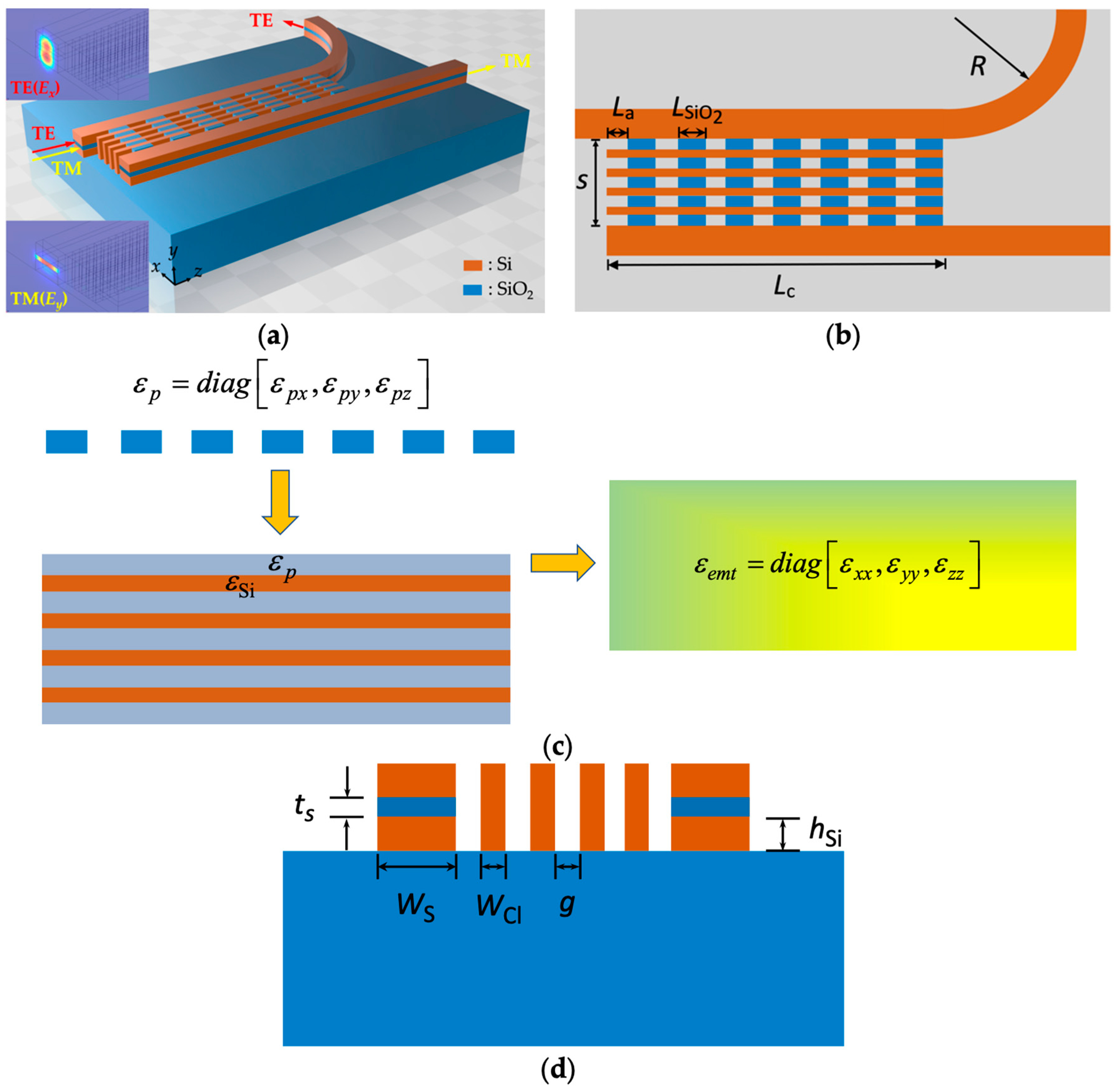
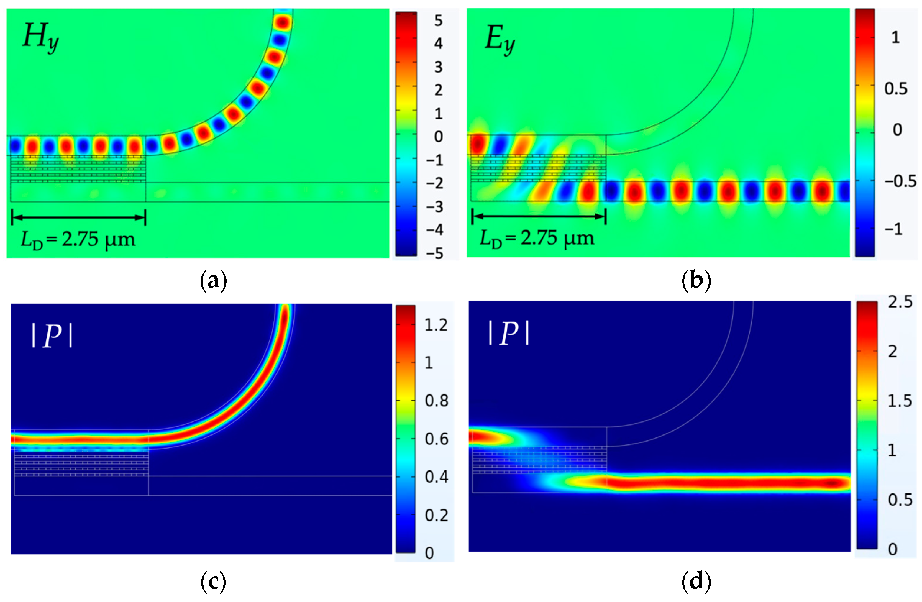
2. Mode Characteristic and Coupling Effect with Anisotropic SWGMs

Figure 1a–c show the 3D diagram with the TE (Ex) and TM (Ey) mode profiles in the incident plane, the top view, and the cross-section in the xy plane, respectively, of the proposed PBS. Slot waveguides on a SiO2 substrate comprised a SiO2 slot layer sandwiched with high-index Si strips in which the TE channel was connected to a bent waveguide with a radius of curvature (R) at the end in order to effectively decouple the two slot waveguides. In the slot waveguides with width WS, the thicknesses of the slot layers and Si layers were ts and hSi, respectively. The height and width of Si strips (copper red) were 2hSi + ts and WS, respectively. The pitch of SWGMs in the x direction was set to Λx = WCl + g with duty cycle ρx = WCl /Λx, where WCl is the width of the Si strips, and g is the gap between Si strips. Edge-to-edge spacing between slot waveguides is s. Likewise, the pitch of SWGMs in the z direction was set to be Λz = La + LSiO2 with duty cycle ρz = LSiO2/Λz, where La is the gap between SiO2 grating (dull blue).
Before analyzing the proposed design, the fabrication processes are schematically illustrated in Figure 2. (1) A negative photoresist (PR) film (purple) was deposited to pattern the lower Si strips with a hard mask defining the patterns of the proposed structure on a SiO2 substrate (blue); then PR exposure and development were conducted. (2) The proposed structure was formed by etching SiO2 and lifting off the PR film. (3) A Si film was deposited by chemical vapor deposition, and the Si layer was planarized by chemical mechanical polishing (CMP). (4) Depositing a positive PR (green) to pattern the SWGMs with another mask was followed by PR exposure and development, SiO2 slot layer deposition using thermal oxidation, and a CMP was conducted. (5) Similar to Step 4 but with a different mask. (6) After SiO2 reactive ion etching, the PR film was lifted off. (7) The upper Si strips and SWGMs were deposited, and a CMP was carried out. (8) A positive PR was deposited with the same mask as that in Step 1, followed by PR exposure and development. (9) After Si etching, the positive PR film was lifted off to reach the desired structure. Lastly, the SiO2 regions between the SWGMs could be formed with the procedures of SiO2 deposition, PR deposition, patterning the 2D SWGMs with a mask, SiO2 etching, and lifting off the PR.
The working principle of the present PBS is that we propagated TE mode with major electric field Ex along the bar, while TM mode was coupled with a major electric field Ey under the phase matching condition (PMC) into the cross, as shown in Figure 1a. Using the EMT [26,27], the proposed 2D SWGMs displayed an equivalent material anisotropy εemt by considering the permittivity of Si, εSi and εp as follows (see Figure 1c):
ε e m t = d i a g [ ε x x , ε y y , ε z z ]
ε x x 1 = ρ x ε Si 1 + ( 1 ρ x ) ε p x 1 ,
ε y y = ρ x ε Si + ( 1 ρ x ) ε p y ,
ε z z = ρ x ε Si + ( 1 ρ x ) ε p z ,
where εxx, εyy, and εzz denote permittivity in the x, y, and z directions, respectively. In this work, εp = diag [εpx, εpy, εpz] denotes the equivalent anisotropic permittivity of the SWGMs consisting of SiO2 strips and air gaps along the z direction, as shown below:
ε p x = ε p y = ρ z ε SiO 2 + ( 1 ρ z ) ε air ,
ε p z 1 = ρ z ε SiO 2 1 + ( 1 ρ z ) ε air 1 ,
where εSiO2 and εair denote the permittivity of SiO2 and air, respectively. Differing from the previous reports [24,25,26,27,28,29,30,31,32,33,34,35,36,37,38,39] using one-dimensional SWGMs, εemt in Equation (1) showed biaxial anisotropy, thus more flexibly tuning the optical characteristics. To design a PBS here, the mode characteristics of the TE and TM modes had to be obtained in advance. After that, the coupling length of a coupled waveguide for a specific mode measuring the distance required to completely transfer power from one waveguide to another can be computed by Lc,i = λ/{2(ni,evenni,odd)} [48], where i denotes TE or TM. ni,even and ni,odd denote the effective indices of the even and odd modes, respectively.
First, we analyzed the mode characteristics of the present design. The relative permittivity of Si and SiO2 was εSi = 12.110 and εSiO2 = 2.085 [49], respectively, at λ = 1550 nm. The chosen parameters were WSi = 400 nm, WCl = 75 nm, g = 50 nm (i.e., ρx = 0.6), hSi = 150 nm, La = 100 nm, LSiO2 = 150 nm (i.e., ρz = 0.6), s = 550 nm, and four Si strips between slot waveguides. First, we obtained the anisotropic εp = diag [1.285, 1.285, 1.206] according to Equations (5) and (6). Next, the resultant biaxially anisotropic εemt = diag [1.851, 2.815, 2.805] could be obtained according to Equations (2)–(4). With the obtained εemt in the region between slot waveguides and using COMSOL Multiphysics 6.0 (COMSOL Inc., Burlington,VT, USA), the coupling length of TM mode Lc,TM and the coupling-length ratio of TE and TM modes Lc,TE/Lc,TM versus ts for the present PBS and the conventional SWs [17,18] are shown in Figure 3. The larger value of Lc,TE/Lc,TM implies that more TE power is retained in the bar while TM power is completely transferred to the cross. Lc,TE was far larger than Lc,TM due to better TE mode confinement; thus, a PBS’s length is determined by a shorter Lc,TM. For conventional SWs [17], Lc,TM (dull blue dotted line) varied from 82.42 to 32.19 μm for ts for 10 and 60 nm, respectively, and Lc,TE/Lc,TM (copper red dotted line) was only 9.16 at ts = 60 nm. In contrast, the proposed structure not only shrunk Lc,TM (dull blue solid line) to 10.69 and 3.15 μm for ts = 10 and 60 nm, respectively, but also improved Lc,TE/Lc,TM (copper red solid line) to 891 at ts = 60 nm. Results demonstrate that the device length and PER of a PBS based on a two-SW can be significantly reduced and improved, respectively, by locating the proposed 2D SWGMs between the two SWs.
Further 3D calculations of mode and propagation characteristics are outlined in the next section. For observing the mode coupling, the even TE and TM field contours of the present structure are exhibited in Figure 4a,b, respectively, and those of the SWs are exhibited in Figure 4c,d, respectively.
By adding 2D SWGs in the middle region of conventional SWs, the decaying rates of evanescent wave of the TE and TM modes are considerably suppressed (i.e., larger Lc,TE/Lc,TM) and enhanced (i.e., shorter Lc,TM), respectively. In addition, the relative field amplitudes of the TE and TM modes along the line denoted in the inset of Figure 4e are shown in Figure 4e,f, respectively. The above results can be explained by the decay constant of the TE mode kTE that can be adjusted by the εzz/εxx ratio according to the dispersion relation [39], and the εzz > εxx condition is always fulfilled. Therefore, 2D SWGMs significantly reduce crosstalk compared to an isotropic cladding with εzz/εxx = 1. In contrast, the decay constant of the TM mode, kTM, depends on the εzz/εyy < 1 ratio, leading to weaker mode confinement.

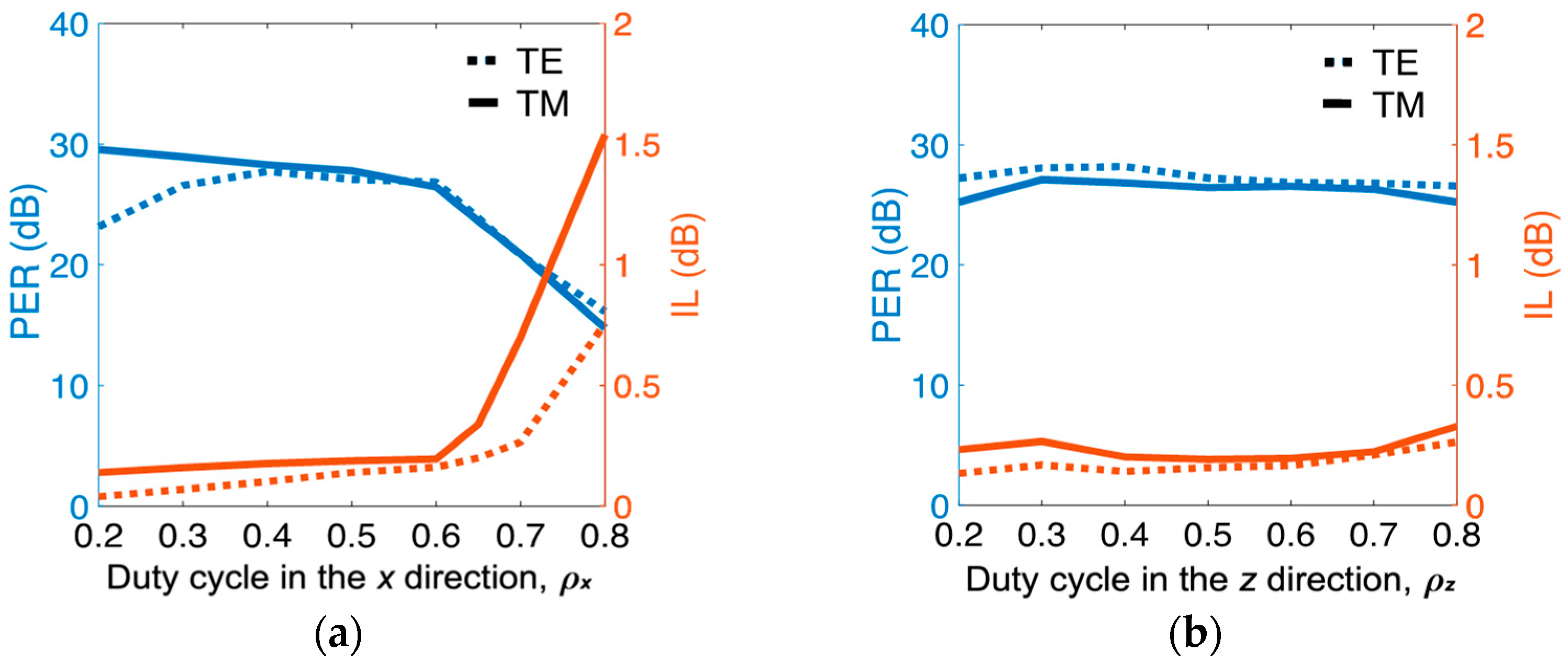
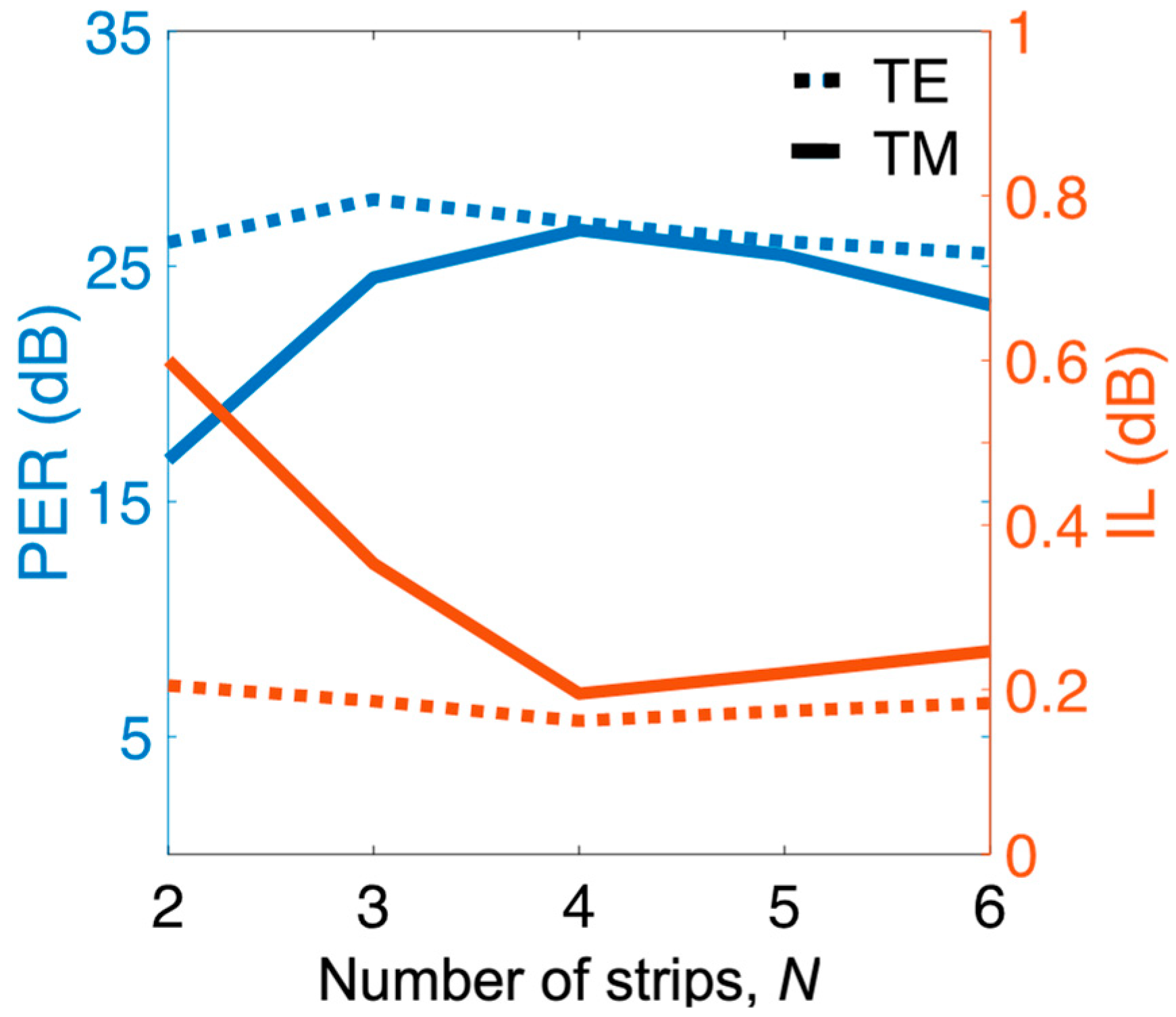
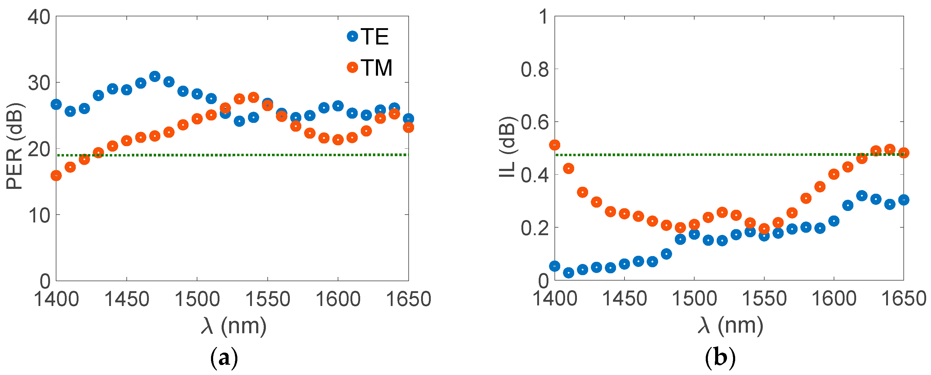
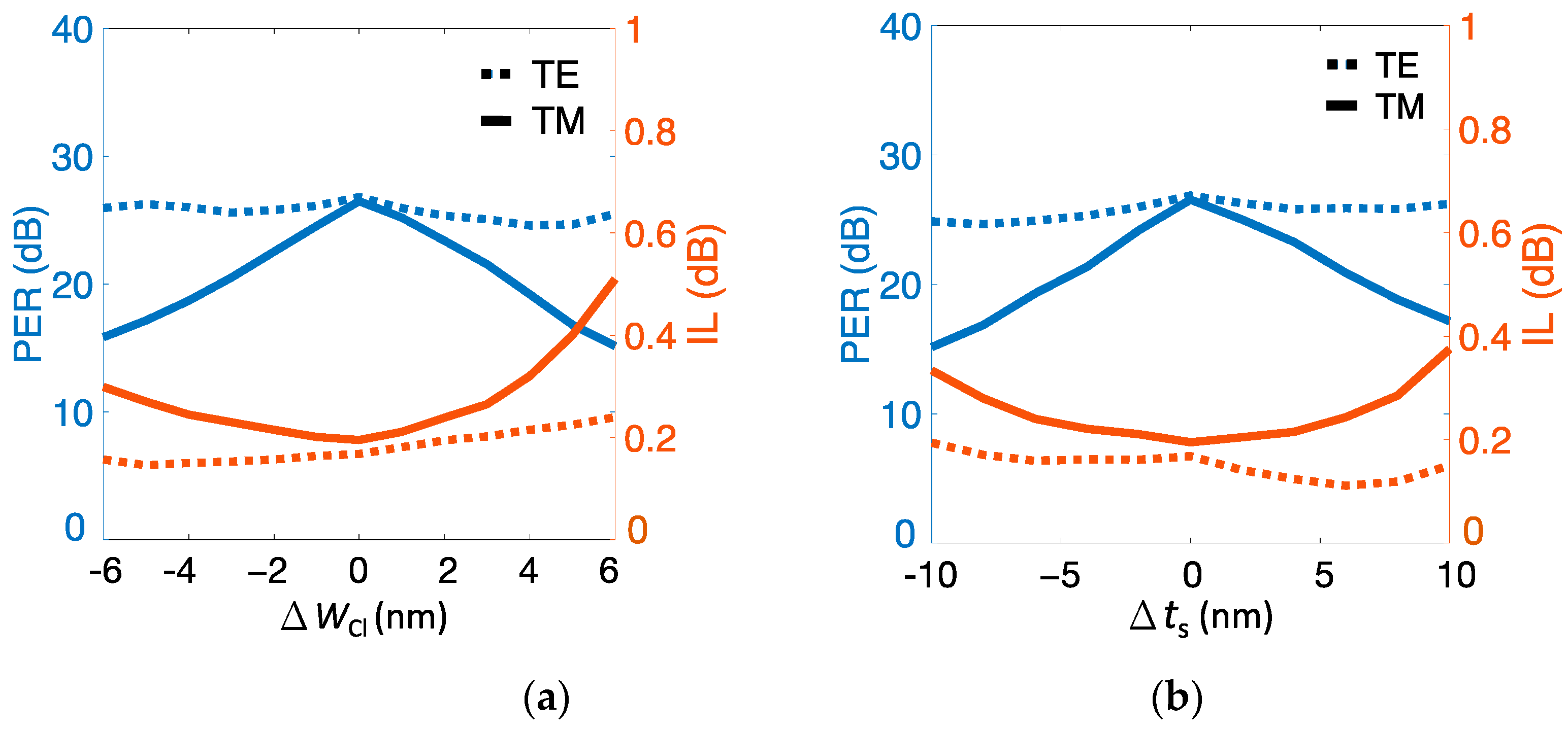
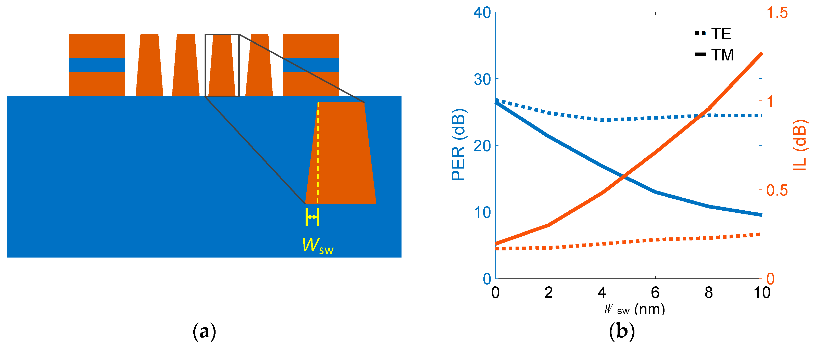
3. Performance Dependences on Duty Cycle, Wavelength, and Fabrication Tolerance

Device performance dependences on geometry parameters, wavelength response, and fabrication tolerance proceeded by executing 3D simulations. To assess the transmission performance of a PBS, we analyze the PERs and ILs of both modes, which are formulated in Equations (7) and (8), respectively:
PER T E ( T M ) = 10 log 10 ( P T E ( T M ) , b a r ( c r o ) P T E ( T M ) , c r o ( b a r ) ) ,
IL T E ( T M ) = 10 log 10 ( P T E ( T M ) , b a r ( c r o ) P i n ) ,
where Pin denotes the input power, PTE(TM),bar(cro) denotes the TE (TM) mode power at the bar (cross), and PTE(TM),cro(bar) is the TE (TM) mode power at the cross (bar). By adopting R = 3 μm and the same parameters displayed in Figure 4, the y component of the magnetic field (Hy) and total power (|P|) evolutions of TE mode are shown in Figure 5a,c, respectively, and the y component of the electric field (Ey) and total power (|P|) evolutions of TM mode are shown in Figure 5b,d, respectively.
In Section 2, the calculated Lc,TM at ts = 60 nm was 3.15 μm on the basis of equivalent permittivity εemt. The practical Lc,TM to obtain optimal performance is device length LD = 2.75 μm, which was shorter than the calculated Lc,TM in Section 2 because the coupling continued a short distance from the entrance of the bent waveguide and then gradually decreased. At device length LD = 2.75 μm, the obtained results were PERTE = 26.81 dB, PERTM = 26.48 dB, ILTE = 0.16 dB, and ILTM = 0.19 dB. By contrast, conventional SWs [17] with Lc,TM = 34.6 μm achieved PERTE = 25.5 dB, PERTM = 14.8 dB, ILTE = 0.07 dB, and ILTM = 0.06 dB. Results show that the proposed PBS not only considerably reduced the proposed PBS’s length by about 12 times when compared to the conventional SWs [17], but also achieved superior PERs, particularly for PERTM. Although the ILs of the current design were higher than those of the SWs, values of <0.2 dB were still acceptable. Considering the effect of duty cycles, we show the PERs and ILs versus ρx in Figure 6a. The optimal PERs and ILs of both modes appeared in the interval of ρx = 0.4 to 0.6. Once the condition of ρx > 0.6 had been reached, PERs and ILs dramatically degraded because a larger ρx decreases (increases) the value of εzz/εxx (εzz/εyy) leading to smaller (larger) kTE (kTM), simultaneously increasing the crosstalk of both modes. The higher PERs are also reflected in lower ILs. Although optimal PERs and ILs were at ρx = 0.4 or 0.5 here, the device length was LD = 6.50 or 4.15 μm, respectively. Considering compactness, we chose ρx = 0.6 to investigate the subsequent analyses, and PERs and ILs versus ρz are exhibited in Figure 6b.
The ILs of the TE and TM modes slightly increased, ranging from ρz = 0.2 (LD = 2.9 μm) to 0.8 (LD = 2.55 μm), and PERTE and PERTM slightly varied as ρz varies. Differing from the major effect of ρx, ρz plays a finetuning role on device performance and length. Regarding to the number of Si strips (N), the PERs and ILs versus N (at the condition of ρx =0.6 and ρz = 0.6) are shown in Figure 7. The proposed PBS achieved optimal performance when N = 4 was chosen. Further increasing N resulted in moderately varying performance. The performance of TM mode dramatically worsened as N decreased. This result can be attributed to t Λx being increasingly away from the condition of Λx << λ, causing the increase in scattering loss that resulted from the grating structure [21].
To assess the BW of the present PBS, the PERs and ILs as a function of wavelength are shown in Figure 8a,b, respectively. PERTM (ILTM) significantly decreased (increased) as the wavelength moved away from the target wavelength of λ = 1550 nm because the short Lc,TM was more sensitive than the extremely long Lc,TE to deviation from the PMC. By contrast, the PERTE and ILTE of the shorter (longer) than λ = 1550 nm wavelengths were higher (lower) and lower (higher), respectively. This can be explained by the guided modes with shorter (longer) wavelengths leading to shorter (longer) evanescent wave tails, thus reducing (increasing) crosstalk between waveguides. The working BW of both modes with PERs > 20 dB and ILs < 0.5 dB ranged from λ = 1440 to 1650 nm (>200 nm).
To show our design’s superiority, we compared its overall performance with that of SWGM-based PBSs, as shown in Table 1. The footprint of the proposed structure was the smallest PBS compared with the reported PBSs [19,20,42,43,44,45,46], rendering it more beneficial in constructing a highly dense photonic component.
In addition to analyzing performance dependence on duty cycles and number of Si strips, as shown in Figure 6 and Figure 7, respectively, we investigated severe geometries ts and WCl to assess fabrication tolerance. Performance versus variations in Si strip width ΔWCl and slot thickness Δts is shown in Figure 9a,b, respectively. PERTM significantly depended on the two fabrication errors (ΔWCl and Δts) because of the extremely short Lc,TM = 2.75 μm of the TM mode. As shown in Figure 9a, PERTM decreased to ~17 dB (from ~26 dB), and ILTM increased to ~0.4 dB (from ~0.2 dB) while ΔWCl > 5 nm or Δts > 10 nm. Within the variation range of ΔWCl < 3 nm or Δts < 5 nm, PERTM maintained values of >20 dB and ILTM < 0.25 dB. In contrast, PERTE and ILTE showed slight variations in ΔWCl and Δts due to the exceptionally long Lc,TE = 891 μm of TE mode.
Another essential fabrication error, angled sidewall, frequently occurs in etching processes that typically do not have a perfect 90° sidewall. In the present structure, the crucial parts are SWGMs due to their larger aspect ratio compared to that of the slot waveguides. Therefore, we now discuss the sidewall effect of the SWGMs on device performance. The width difference between the bottom and top of the SWGMs is Wsw, as shown in Figure 10a, and the PERs and ILs of both modes are shown in Figure 10b. PERTE (PERTM) and ILTE (ILTM) showed slight (significant) dependences on Wsw due to the extremely weak (strong) coupling strength induced by the 2D SWGMs. PERTM decreased to about 14.2 (9.8) dB, and ILTM increased to about 0.62 (1.25) dB, while Wsw increased to 5 (10) nm.

4. Conclusions

An ultracompact and broadband PBS comprising slot waveguides assisted by in between 2D SWGMs was proposed to increase the integration density and transmission bandwidth of photonic devices. The proposed 2D SWGMs served as both a barrier to suppress TE mode coupling and bridging to improve TM mode coupling by carefully engineering the duty cycles of the SWGMs. The numerical results of the proposed PBS showed PERs of 26.8 and 26.4 dB for TE and TM modes, respectively, and ILs of ~0.25 dB for both modes, with a compact PBS of 1.35 μm × 2.75 μm. Moreover, the present PBS achieved satisfactory performance while operating in a BW of 200 nm. Fabrication tolerance analyses showed that the PERTM maintained superior values of >20 dB and ILTM < 0.25 dB within the variation range of clad width ΔWCl < 3 nm or slot thickness Δts < 5 nm.

Author Contributions

All authors conceived the designed idea and discussed the results; R.-J.C. performed the numerical simulations; C.-C.H. wrote the manuscript and supervised the whole work. All authors have read and agreed to the published version of the manuscript.

Funding

This research was funded by the Ministry of Science and Technology (MOST) of Taiwan, which financially supported this research under grant number 110-2112-M-005-005.

Institutional Review Board Statement

Not applicable.

Informed Consent Statement

Not applicable.

Data Availability Statement

Data presented in this study are available on request from the corresponding author.

Acknowledgments

The authors would like to thank Mon-Shu Ho and Yen-Fu Lin in the Institute of Nanoscience, National Chung Hsing University for the discussions of the fabrication processes.

Conflicts of Interest

The authors declare no conflict of interest.

References

  1. Dai, D.; Bauters, J.; Bowers, J.E. Passive technologies for future large-scale photonic integrated circuits on silicon: Polarization handling, light non-reciprocity and loss reduction. Light-Sci. Appl. 2012, 1, 12. [Google Scholar] [CrossRef]
  2. Dai, D.; Liu, L.; Gao, S.; Xu, D.X.; He, S. Polarization management for silicon photonic integrated circuits. Laser Photonics Rev. 2013, 7, 303–328. [Google Scholar] [CrossRef]
  3. Rahim, A.; Spuesens, T.; Baets, R.; Bogaerts, W. Open-access silicon photonics: Current status and emerging initiatives. Proc. IEEE 2018, 106, 2313–2330. [Google Scholar] [CrossRef] [Green Version]
  4. Bogaerts, W.; Chrostowski, L. Silicon photonics circuit design: Method, tools, and challenges. Laser Photonics Rev. 2018, 12, 1700237. [Google Scholar] [CrossRef]
  5. Beggs, D.M.; Midrio, M.; Krauss, T.F. Compact polarization rotators for integrated polarization diversity in InP-based waveguides. Opt. Lett. 2007, 32, 2176–2178. [Google Scholar] [CrossRef]
  6. Alonso-Ramos, C.; Romero-García, S.; Ortega-Moñux, A.; Molina-Fernández, I.; Zhang, R.; Bach, H.G.; Schell, M. Polarization rotator for InP rib waveguide. Opt. Lett. 2012, 37, 335–337. [Google Scholar] [CrossRef]
  7. Hsu, C.W.; Lin, H.Y.; Chen, J.Y.; Cheng, Y.C. Ultracompact polarization rotator in an asymmetric single dielectric loaded rib waveguide. Appl. Opt. 2016, 55, 1395–1400. [Google Scholar] [CrossRef]
  8. Vakarin, V.; Ye, W.N.; Ramírez, J.M.; Liu, Q.; Frigerio, J.; Ballabio, A.; Isella, G.; Vivien, L.; Alonso-Ramos, C.; Cheben, P.; et al. Ultra-wideband Ge-rich silicon germanium mid-infrared polarization rotator with mode hybridization flattening. Opt. Express 2019, 27, 9838–9847. [Google Scholar] [CrossRef]
  9. Ying, Z.; Wang, G.; Zhang, X.; Huang, Y.; Ho, H.P.; Zhang, Y. Ultracompact TE-pass polarizer based on a hybrid plasmonic waveguide. IEEE Photonics Technol. Lett. 2015, 27, 201–204. [Google Scholar] [CrossRef]
  10. de Oliveira, R.; de Matos, C. Graphene based waveguide polarizers: In-depth physical analysis and relevant parameters. Sci Rep. 2015, 5, 16949. [Google Scholar] [CrossRef] [Green Version]
  11. Ni, B.; Xiao, J.B. Broadband TE-pass slot waveguide polarizer using an asymmetrical directional coupler. Appl. Opt. 2018, 57, 4032–4038. [Google Scholar] [CrossRef] [PubMed]
  12. Ni, B.; Xiao, J.B. Subwavelength-grating-based compact and broadband TE-pass polarizer for slot waveguides on a SOI platform. J. Opt. Soc. Am. B 2019, 36, 2126–2133. [Google Scholar] [CrossRef]
  13. Lin, B.; Lian, T.; Sun, S.; Zhu, M.; Che, Y.; Sun, X.; Wang, X.; Zhang, D. Ultra-broadband and compact TM-pass polarizer based on graphene-buried polymer waveguide. Polymers 2022, 14, 1481. [Google Scholar] [CrossRef] [PubMed]
  14. Fukuda, H.; Yamada, K.; Tsuchizawa, T.; Watanabe, T.; Shinojima, H.; Itabashi, S. Ultrasmall polarization splitter based on silicon wire waveguides. Opt. Express 2013, 14, 12401–12408. [Google Scholar] [CrossRef]
  15. Guan, X.; Wu, H.; Shi, Y.; Wosinski, L.; Dai, D. Ultracompact and broadband polarization beam splitter utilizing the evanescent coupling between a hybrid plasmonic waveguide and a silicon nanowire. Opt. Lett. 2013, 38, 3005–3008. [Google Scholar] [CrossRef]
  16. Guan, X.; Wu, H.; Shi, Y.; Dai, D. Extremely small polarization beam splitter based on a multimode interference coupler with a silicon hybrid plasmonic waveguide. Opt. Lett. 2014, 39, 259–262. [Google Scholar] [CrossRef]
  17. Yue, Y.; Zhang, L.; Yang, J.Y.; Beausoleil, R.G.; Willner, A.E. Silicon-on-insulator splitter using two horizontally slotted waveguides. Opt. Lett. 2010, 35, 1364–1366. [Google Scholar] [CrossRef]
  18. Zhang, H.; Huang, Y.; Das, S.; Li, C.; Yu, M.; Lo, P.G.Q.; Hong, M.; Thong, J. Polarization splitter using horizontal slot waveguide. Opt. Express 2013, 21, 3363–3369. [Google Scholar] [CrossRef]
  19. Kim, D.W.; Lee, M.H.; Kim, Y.; Kim, K.H. Planar-type polarization beam splitter based on a bridged silicon waveguide coupler. Opt. Express 2015, 23, 998–1004. [Google Scholar] [CrossRef]
  20. Kim, Y.; Lee, M.H.; Kim, Y.; Kim, K.H. High-extinction-ratio directional-coupler-type polarization beam splitter with a bridged silicon wire waveguide. Opt. Lett. 2018, 43, 3241–3244. [Google Scholar] [CrossRef]
  21. Almeida, V.R.; Xu, Q.; Barrios, C.A.; Lipson, M. Guiding and confining light in void nanostructure. Opt. Lett. 2004, 29, 1209–1211. [Google Scholar] [CrossRef] [PubMed]
  22. Xu, Q.; Almeida, V.R.; Panepucci, R.R.; Lipson, M. Experimental demonstration of guiding and confining light in nanometer-size low-refractive-index material. Opt. Lett. 2004, 29, 1626–1628. [Google Scholar] [CrossRef] [PubMed]
  23. Halir, R.; Bock, P.J.; Cheben, P.; Ortega-Moñux, A.; Alonso-Ramos, C.; Schmid, J.H.; Lapointe, J.; Xu, D.X.; Wangüemert-Pérez, J.G.; Molina-Fernández, Í.; et al. Waveguide sub-wavelength structures: A review of principles and applications. Laser Photonics Rev. 2015, 9, 25–49. [Google Scholar] [CrossRef]
  24. Halir, R.; Ortega-Moñux, A.; Benedikovic, D.; Mashanovich, G.Z.; Wangüemert-Pérez, J.G.; Schmid, J.H.; Molina-Fernández, Í.; Cheben, P. Subwavelength-grating metamaterial structures for silicon photonic devices. Proc. IEEE 2018, 106, 2144–2156. [Google Scholar] [CrossRef] [Green Version]
  25. Cheben, P.; Halir, R.; Schmid, J.H.; Atwater, H.A.; Smith, D.R. Subwavelength integrated photonics. Nature 2018, 560, 565–572. [Google Scholar] [CrossRef]
  26. Gu, C.; Yeh, P. Form birefringence dispersion in periodic layered media. Opt. Lett. 1996, 21, 504–506. [Google Scholar] [CrossRef]
  27. Lalanne, P.; Lemercier-Lalanne, D. Depth dependence of the effective properties of subwavelength gratings. J. Op. Soc. Am. A 1997, 14, 450–458. [Google Scholar] [CrossRef]
  28. Wang, Y. Compact broadband directional couplers using subwavelength gratings. IEEE Photonics J. 2016, 8, 7101408. [Google Scholar] [CrossRef]
  29. Yun, H.; Wang, Y.; Zhang, F.; Lu, Z.; Lin, S.; Chrostowski, L.; Jaeger, N.A.F. Broadband 2 × 2 adiabatic 3 dB coupler using silicon-on-insulator sub-wavelength grating waveguides. Opt. Lett. 2016, 41, 3041–3044. [Google Scholar] [CrossRef]
  30. Benedikovic, D.; Cheben, P.; Schmid, J.H.; Xu, D.X.; Lapointe, J.; Wang, S.; Halir, R.; Ortega-Moñux, A.; Janz, S.; Dado, M. High-efficiency single etch step apodized surface grating coupler using subwavelength structure. Laser Photonics Rev. 2014, 8, 93–97. [Google Scholar] [CrossRef]
  31. Zhu, L.; Yang, W.; Chang-Hasnain, C. Very high efficiency optical coupler for silicon nanophotonic waveguide and single mode optical fiber. Opt. Express 2017, 25, 18462–18473. [Google Scholar] [CrossRef]
  32. Čtyroký, J.; Wangüemert-Pérez, J.G.; Kwiecien, P.; Richter, I.; Litvik, J.; Schmid, J.H.; Molina-Fernández, Í.; Ortega-Moñux, A.; Dado, M.; Cheben, P. Design of narrowband Bragg spectral filters in subwavelength grating metamaterial waveguides. Opt. Express 2018, 26, 179–194. [Google Scholar] [CrossRef] [PubMed] [Green Version]
  33. Naghdi, B.; Chen, L.R. Spectral engineering of subwavelength- grating-based contradirectional couplers. Opt. Express 2017, 25, 25310–25317. [Google Scholar] [CrossRef] [PubMed]
  34. Halir, R.; Cheben, P.; Luque-González, J.M.; Sarmiento-Merenguel, J.D.; Schmid, J.H. Ultra-broadband nanophotonic beamsplitter using an anisotropic sub-wavelength metamaterial. Laser Photonics Rev. 2016, 10, 1039–1046. [Google Scholar] [CrossRef]
  35. Xu, Y.; Xiao, J. Compact and high extinction ratio polarization beam splitter using subwavelength grating couplers. Opt. Lett. 2016, 41, 773–776. [Google Scholar] [CrossRef]
  36. Liu, L.; Deng, Q.; Zhou, Z. Manipulation of beat length and wavelength dependence of a polarization beam splitter using a subwavelength grating. Opt. Lett. 2016, 41, 5126–5129. [Google Scholar] [CrossRef]
  37. Xu, H.; Shi, Y. Ultra-sharp multi-mode waveguide bending assisted with metamaterial-based mode converters. Laser Photonics Rev. 2018, 12, 1700240. [Google Scholar] [CrossRef]
  38. Luque-González, J.M.; Herrero-Bermello, A.; Ortega-Moñux, A.; Sánchez-Rodríguez, M.; Velasco, A.V.; Schmid, J.H.; Cheben, P.; Molina-Fernández, Í.; Halir, R. Polarization splitting directional coupler using tilted subwavelength gratings. Opt. Lett. 2020, 45, 5126–5129. [Google Scholar] [CrossRef]
  39. Jahani, S.; Jacob, Z. Transparent subdiffraction optics: Nanoscale light confinement without metal. Optica 2014, 1, 96–100. [Google Scholar] [CrossRef]
  40. Jahani, S.; Kim, S.; Atkinson, J.; Wirth, J.C.; Kalhor, F.; Noman, A.A.; Newman, W.D.; Shekhar, P.; Han, K.; Van, V.; et al. Controlling evanescent waves using silicon photonic all-dielectric metamaterials for dense integration. Nat. Commun. 2018, 9, 1893. [Google Scholar] [CrossRef]
  41. Mia, M.B.; Ahmed, S.Z.; Ahmed, I.; Lee, Y.J.; Qi, M.; Kim, S. Exceptional coupling in photonic anisotropic metamaterials for extremely low waveguide crosstalk. Optica 2020, 7, 881–887. [Google Scholar] [CrossRef]
  42. Li, C.; Zhang, M.; Bowers, J.E.; Dai, D. Ultra-broadband polarization beam splitter with silicon subwavelength-grating waveguides. Opt. Lett. 2020, 45, 2259–2262. [Google Scholar] [CrossRef] [PubMed]
  43. Mao, S.; Cheng, L.; Zhao, C.; Fu, H.Y. Ultra-broadband and ultra-compact polarization beam splitter based on a tapered subwavelength-grating waveguide and slot waveguide. Opt. Express 2021, 29, 28066–28077. [Google Scholar] [CrossRef] [PubMed]
  44. Mia, M.B.; Ahmed, S.Z.; Jaidye, N.; Ahmed, I.; Kim, S. Mode-evolution-based ultra-broadband polarization beam splitter using adiabatically tapered extreme skin-depth waveguide. Opt. Lett. 2021, 46, 4490–4493. [Google Scholar] [CrossRef] [PubMed]
  45. Zhang, J.; Shi, X.; Zhang, Z.; Guo, K.; Yang, J. Ultra-compact, efficient and high-polarization-extinction-ratio polarization beam splitters based on photonic anisotropic metamaterials. Opt. Express 2022, 30, 538–549. [Google Scholar] [CrossRef] [PubMed]
  46. Xu, H.; Dai, D.; Shi, Y. Ultra-broadband and ultra-compact on-chip silicon polarization beam splitter by using hetero-anisotropic metamaterials. Laser Photonics Rev. 2019, 13, 1800349. [Google Scholar] [CrossRef]
  47. Niekerk, M.V.; Jahani, S.; Bickford, J.; Cho, P.; Anderson, S.; Leake, G.; Coleman, D.; Fanto, M.L.; Tison, C.C.; Howland, G.A.; et al. Two-dimensional extreme skin depth engineering for CMOS photonics. J. Opt. Soc. Am. B 2021, 38, 1307–1316. [Google Scholar] [CrossRef]
  48. Huang, W.P. Coupled-mode theory for optical waveguides: An overview. J. Opt. Soc. Am. A 1994, 11, 963–983. [Google Scholar] [CrossRef]
  49. Bass, M.; DeCusatis, C.; Enoch, J.; Lakshminarayanan, V.; Li, G.; MacDonald, C.; Mahajan, V.; StrylandBass, E.V. Handbook of Optics, Third Edition Volume IV: Optical Properties of Materials, Nonlinear Optics, Quantum Optics; McGraw-Hill: New York, NY, USA, 2009. [Google Scholar]
Figure 1. (a) 3D diagram with TE (Ex) and TM (Ey) mode profiles in the incident plane; (b) top view; (c) schematic of calculating the resultant effective permittivity εemt of 2D SWGMs, which is obtained by sequentially estimating the 1D SWGMs in the z (εp) and x directions (εemt) on the basis of EMT between slot waveguides; (d) cross-section in xy plane of the present PBS.
Nanomaterials 12 01852 g001
Figure 2. Schematic diagram of the fabrication processes of the designed PBS.
Nanomaterials 12 01852 g002
Figure 3. (left axis) Coupling length of TM mode Lc,TM TM and (right axis) coupling-length ratio Lc,TE/Lc, versus ts for the present PBS and the SWs.
Nanomaterials 12 01852 g003
Figure 4. Field contours of the even modes of (a) TE and (b) TM and those of (c) TE and (d) TM of the SWs for WSi = 400 nm, ts = 60 nm, hSi = 150 nm, WCl = 75 nm, g = 50 nm, s = 550 nm, and λ = 1550 nm. (e) Field amplitudes at the central lines of the slot along the x directions of (a,c); (f) field amplitudes at the central lines of the slot along the x directions of (b,d).
Nanomaterials 12 01852 g004aNanomaterials 12 01852 g004b
Figure 5. y components of (a) magnetic field of the TE mode and (b) electric field of the TM mode, and the total power evolutions of the (c) TE and (d) TM modes of the present structure with device length LD = 2.75 μm (i.e., the practical Lc,TM with optimal performance) for ts = 60 nm, hSi = 150 nm, WCl = 75 nm, WSi = 400 nm, g = 50 nm, s = 550 nm, and λ = 1550 nm.
Nanomaterials 12 01852 g005
Figure 6. (left axis) PER and (right axis) IL of both modes as functions of duty cycles (a) ρx and (b) ρz at the same parameters as those in Figure 4.
Nanomaterials 12 01852 g006
Figure 7. (left axis) PER and (right axis) IL of both modes as a function of the number of Si strips, N between slot waveguides at the same parameters as those in Figure 5.
Nanomaterials 12 01852 g007
Figure 8. (a) PER and (b) IL versus wavelength at the same parameters as those in Figure 4.
Nanomaterials 12 01852 g008
Figure 9. (left axis) PER and (right axis) IL as functions of variations in the (a) Si strip width ΔWCl and (b) slot thickness Δts of the present structure.
Nanomaterials 12 01852 g009
Figure 10. (a) Cross-sectional diagram in xy plane and zooned-in view of a SWGM, where Wsw denotes the difference between the bottom and top of the SWGMs. (b) PER and IL versus Wsw.
Nanomaterials 12 01852 g010
Table 1. Performance comparison of SWGM-based PBSs.
StructureFootprint (μm2)PERs (dB)ILs (dB)BW (nm)
[19]1.7 × 12.2522.51.8>100
[20]2.41 × 29.439.00.35>100
[42]2.5 × 33.6200.3270
[43]1.3 × 4.610.90.8420
[44]2.75 × 100201.2250
[45]2.5 × 1420180
[46]1.9 × 12.25201200
This work1.35 × 2.75200.5200
Publisher’s Note: MDPI stays neutral with regard to jurisdictional claims in published maps and institutional affiliations.

