

Recent Progress of Two-Dimensional Materials for Ultrafast Photonics


Abstract
:1. Introduction
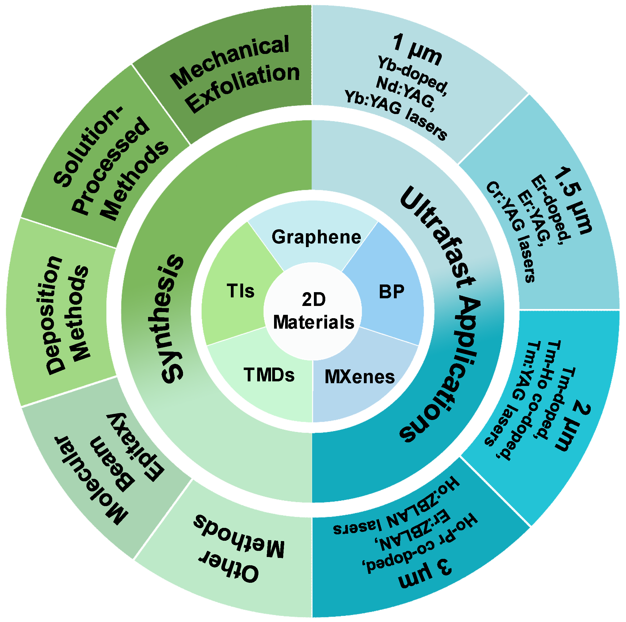
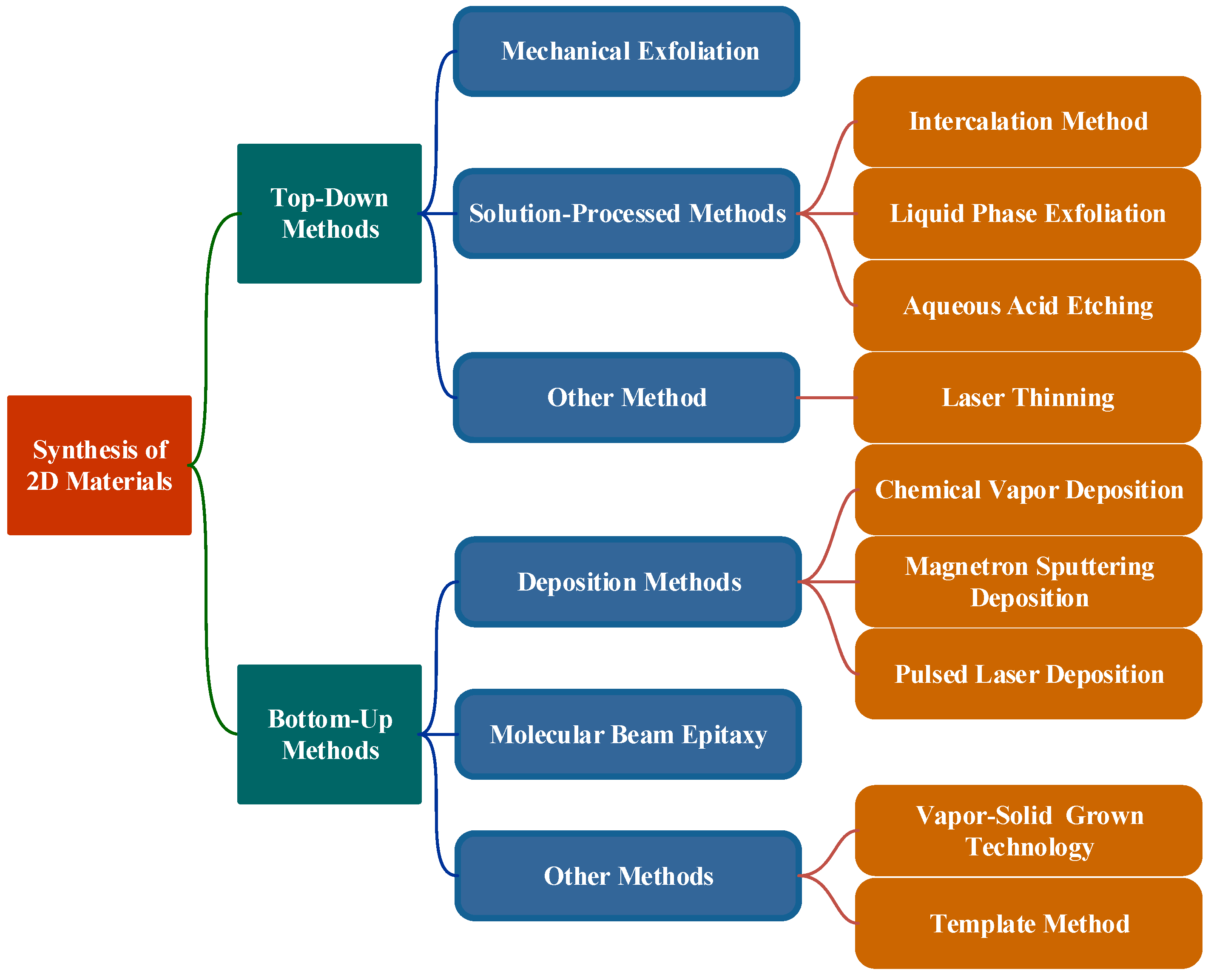
2. Synthesis
2.1. Top-Down Methods
2.1.1. Mechanical Exfoliation
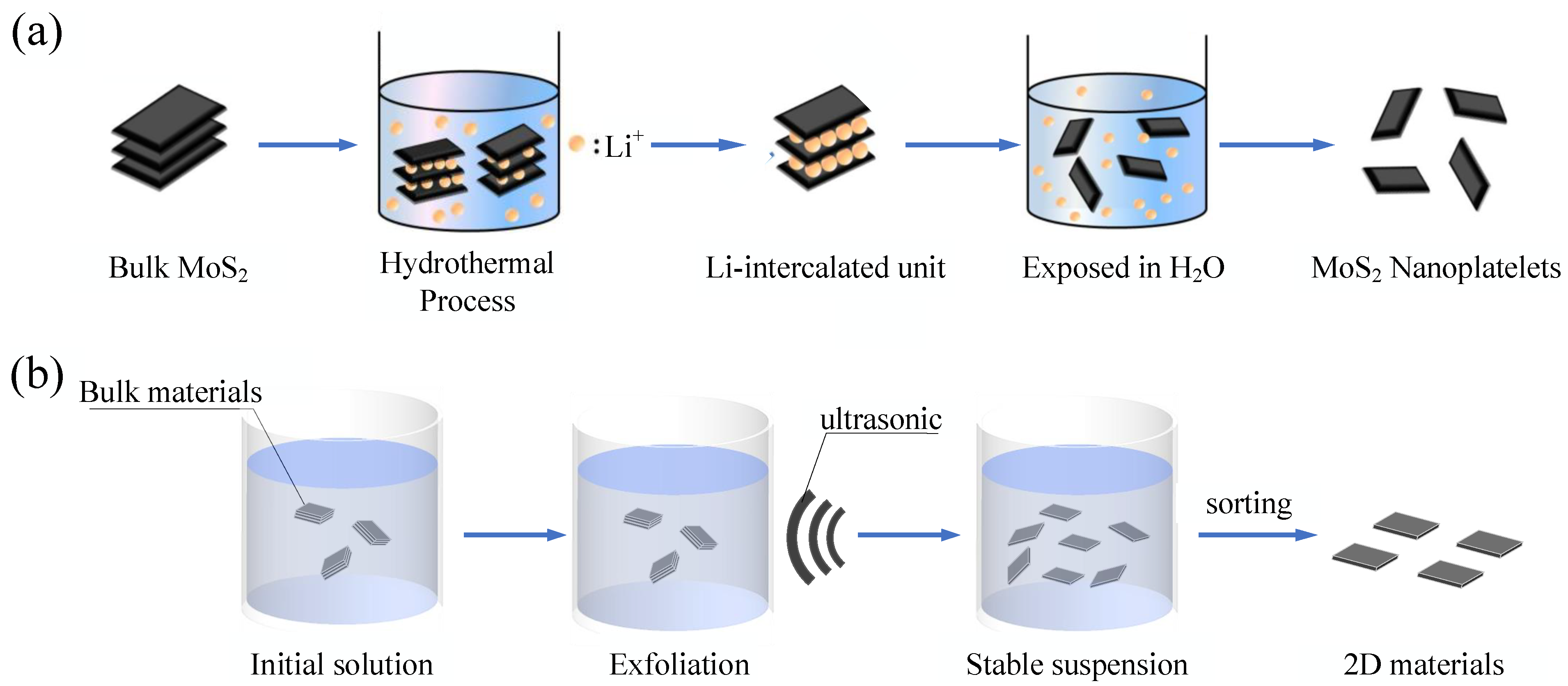
2.1.2. Solution-Processed Methods
2.1.3. Other Methods
2.2. Bottom-Up Methods
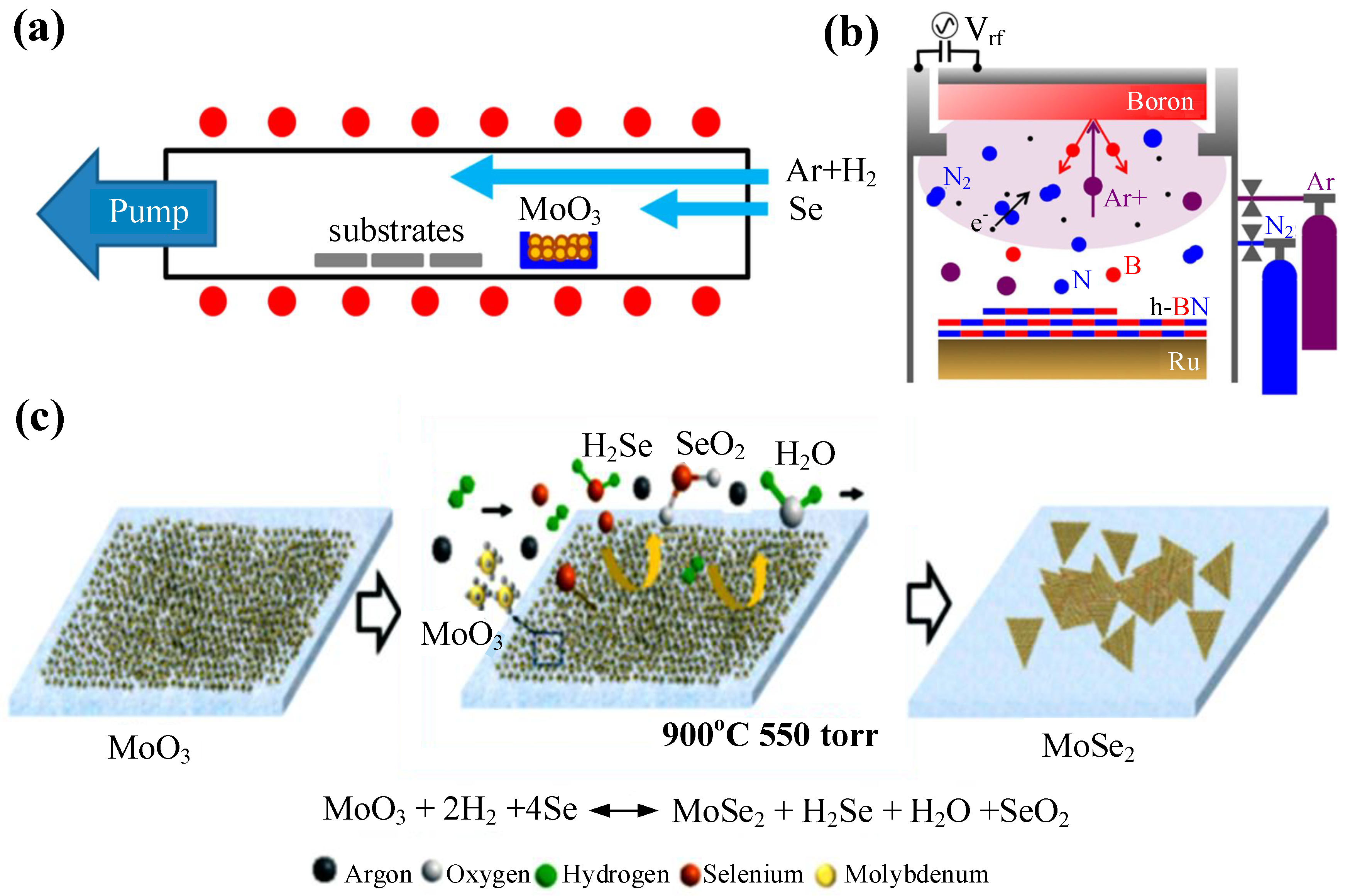
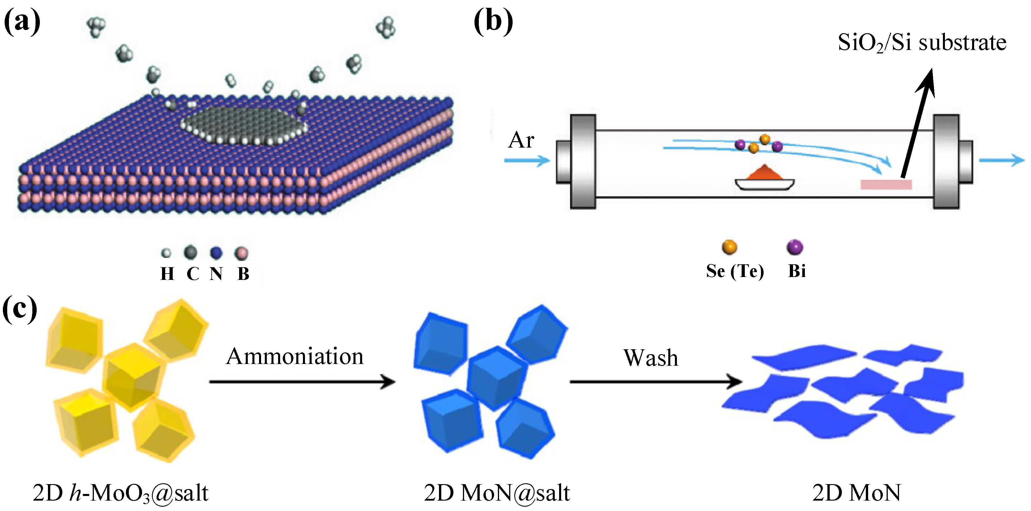
2.2.1. Deposition Methods
2.2.2. Molecular Beam Epitaxy
2.2.3. Other Methods
3. Applications of 2D Materials in Ultrafast Lasers
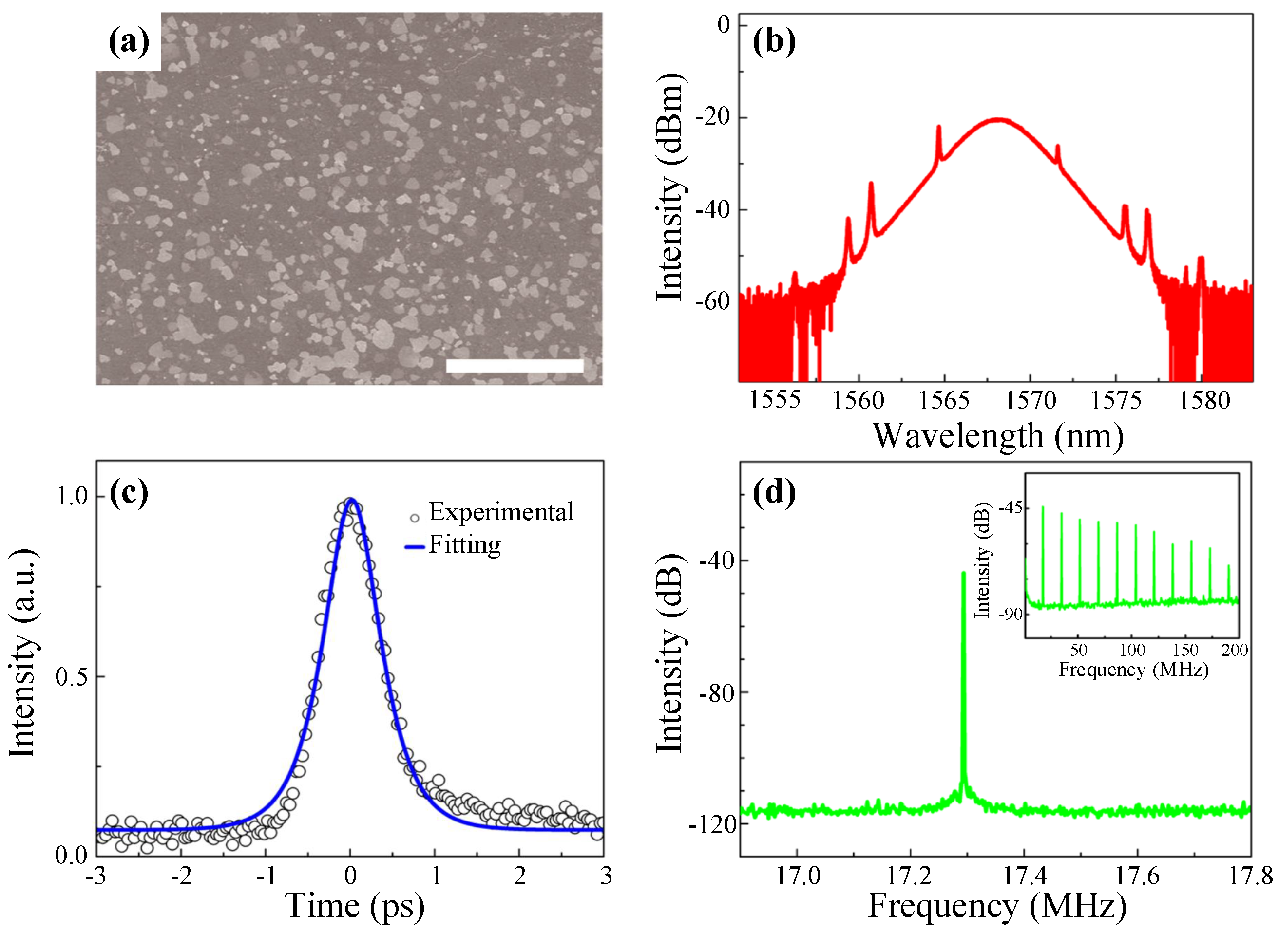
3.1. Graphene
3.2. Topological Insulators
3.3. Transition Metal Dichalcogenides
3.4. Black Phosphorus
3.5. MXenes
3.6. Heterostructures

| 2D Materials | Fabrication Methods | Gain Media | (nm) | (s) | (Hz) | Energy (nJ) | Power (mW) | SNR (dB) | Ref. | |
|---|---|---|---|---|---|---|---|---|---|---|
| Graphene | Graphene | CVD | Alexandrite | 750 | 65 f | 5.56 M | 1.4 | 8 | 75 | [364] |
| Graphene | CVD | Yb | 1069.8 | 580 p | 0.9 M | 0.41 | 0.37 | 70 | [201] | |
| Graphene | MBE | Nd:YAG | 1064 | 161 n | 660 k | 159.2 | 105 | – | [200] | |
| Graphene | LPE | Er | 1525 | ∼1.15 p | ∼8 M | ∼125 p | ∼1 | ∼80 | [188] | |
| Graphene | Modified Hummers | Er | 1566.2, 1566.4 | 3.7 | 3.3–65.9 k | 16.7 | 1.1 | – | [39] | |
| Graphene | ME | Er | 1560.5 | 900 f | 2.22 G | 4.3 p | 9.6 | 50 | [196] | |
| Graphene | LPE | Er | 1550 | ∼29 f | 18.67 M | 2.8 | 52 | 62 | [368] | |
| Graphene | CVD | Tm:CLNGG | 2018 | 729 f | 98.7 M | 0.6 | 60.2 | – | [206] | |
| Graphene | CVD | Tm | 2007.1, 2010.4 | 1.4 | 44–53 k | 85 | 4.5 | 40 | [208] | |
| Graphene | LPE | Tm | 1940 | 3.6 p | 6.46 M | ∼0.4 | ∼2 | ∼70 | [207] | |
| Graphene | CVD | Tm | 1897.7 | 122 n | 0.964 M | 35.2 | 34 | 67 | [209] | |
| Graphene | CVD | Yb | 1035 | 6.5 n | 16.29 M | 0.81 | 13 | 55 | [55] | |
| Er | 1564 | 870 f | 19.30 M | 10.4 p | 0.2 | 64 | ||||
| Tm-Ho | 1908 | 65 n | 1.82 M | 16.2 | 29 | 60 | ||||
| Graphene | – | Er-doped ZBLAN | 2783 | 2.9 | 18.9–37.2 k | 0.74–1.67 | 15–62 | 30 | [361] | |
| Graphene | CVD | Er-doped ZBLAN | 2784.5 | 42 p | 25.4 M | 0.7 | 18 | 43.5 | [214] | |
| TIs | BiSe | LPE | Pr-doped ZBLAN | 635.5, 635.7 | 244–761 n | 191.6–454.5 k | 22.3 | 7.6 | ∼43 | [243] |
| BiSe | LPE | Yb | 1067.66 | 1.95 | 8.3–29.1 k | 17.9 | 0.46 | 48 | [226] | |
| BiSe | PM | Yb | 1031.7 | 46 p | 44.6 M | 0.756 | 33.7 | 58 | [88] | |
| BiSe | PM | Er | 1565.1 | 14 | 8.865 k | 12.6 | 112 | – | [86] | |
| BiSe | ME | Tm-Ho | 1912.12 | 853 f | ∼18.37 M | – | – | 65 | [234] | |
| BiSe | LPE | Tm | 1980 | 4.18 | 8.4–26.8 k | 313 | 8.4 | 43 | [231] | |
| BiSe | LPE | Ho-doped ZBLAN | 2920.6 | 1.54–3.47 | 24.97–56.13 k | 6 | 315 | ∼43 | [239] | |
| BiTe | ME | Yb | 1057.82 | 230 p | 1.44 M | 0.599 | 0.86 | ∼77 | [227] | |
| BiTe | Spin coating- co-reduction | Nd:YVO | 1064 | 7.9 p | 949 M | 0.1 n | 181 | 61 | [230] | |
| BiTe | ME | Nd:YVO | 1064 | 97 n | 47 k | 0.6 | 26.1 | – | [229] | |
| Nd:YVO | 1342 | 93 n | 75 k | 0.4 | 33.2 | |||||
| BiTe | HI/E | Er:YAG | 1645 | 6.3 | 40.7 k | 5.3 | 210 | – | [46] | |
| BiTe | LPE | Er | 1566.9 | 14 | 6.97 k | – | – | 36.4 | [369] | |
| BiTe | PLD | Er | 1562.4 | 920 f | 2.95 G | 15.4 p | 45.3 | 60 | [221] | |
| BiTe | HI/E | Ho-doped ZBLAN | 2979.9 | 1.37–4.83 | 46.20–81.96 k | 3.99 | 327.38 | 37.4 | [237] | |
| SbTe | ME | Er | 1565 | 128 f | 22.32 M | 44.8 p | 1 | 65 | [220] | |
| SbTe | MSD | Er | 1558 | 167 f | 25.38 M | 0.21 | 5.34 | 68 | [222] | |
| CoSb | – | Er | 1557.9 | ∼833 f | 14.48 M | 6.9 p | 0.1 | 57 | [370] | |
| TMDs | MoS | HI/E | Yb | 1054.3 | 800 p | 6.58 M | 1.41 | 9.3 | 50 | [47] |
| MoS | LPE | Nd:YAP | 1079.5 | 227–580 n | 32–232.5 k | 1.11 | 0.26 | – | [254] | |
| MoS | CVD | Er | 1568 | 4.98 p | 26.02 M | – | – | 63 | [258] | |
| Er | 1568 | 637 f | 33.48 M | 61 | ||||||
| MoS | LPE | Er | 1551.2 | 5.7 | 16.78 k | – | – | ∼50 | [257] | |
| MoS | LPE | Yb | 1066.5 | 5.8 | 6.4–28.9 k | 32.6 | 0.9 | 44.6 | [268] | |
| Er | 1565 | 5.4–23.2 | 6.5–27.0 k | 63.2 | 1.7 | 54.5 | ||||
| Tm | 2032 | 1.76 | 33.6–48.1 k | ∼1 | 47.3 | 54.6 | ||||
| MoS | LPE | Er-doped ZBLAN | 2754 | 1.84 –806 n | 36–70 k | 1–2 | 37–140 | 40 | [362] | |
| WS | Chemical weathering exfoliation | Yb:YAG | 1057.5 | 736 f | 86.7 M | 3.11 | 27 | ∼51 | [251] | |
| WS | LPE | Nd:YAG | 1064.5 | 1.28–2.36 | 28.59–45.25 k | 1.2 | 54 | – | [254] | |
| WS | CVD | Er | 1557.4 | 163.5 f | 63.133 M | 0.45 | 28.5 | 96 | [371] | |
| WS | PLD | Er | 1559.7 | 452 f | 1.04 G | 10.87 p | 11.3 | 48 | [360] | |
| WS | LPE | Tm-Ho | 1941 | 1.3 p | 34.8 M | ∼17.2 p | ∼0.6 | 72 | [271] | |
| WS | Sulfidation grown | Ho/Pr co-doped ZBLAN | 2865.7 | 1.73–3.8 | 25.6–131.6 k | 0.17–0.42 | 4–48.4 | 40.5 | [275] | |
| BP | BP | LPE | Yb:CYA | 1064 | 620 n–1.2 | ∼87.7–113.6 k | 182.4–325.7 | 16-37 | – | [292] |
| MoSe | CVD | Nd:YAG | 1064 | 80–290 n | 0.995–3.334 M | 35.9 | 115.1 | – | [253] | |
| WSe | CVD | Nd:YAG | 1064 | 52–400 n | 0.781–2.938 M | 19 | 45.7 | – | ||
| WSe | CVD | Tm | 1863.96 | 1.16 p | 11.36 M | 2.89 | 32.5 | 53 | [273] | |
| PtSe | CVD | Ho/Pr co-doped ZBLAN | 2865 | 620 n–1.72 | 104.2–238.1 k | 0.14–0.39 | 15-93 | 30 | [372] | |
| BP | LPE | Yb, Lu:CALGO | 1053.4 | 272 f | 63.3 M | 6.48 | 0.82 | ∼62 | [294] | |
| BP | ME | Yb | 1038.7, 1042.1 | 1.16–2.05 | 52.52–58.73 k | 2.09 | 0.12 | 50 | [295] | |
| BP | ME | Er | 1532.5 | 9.5–3.1 | 26–40 k | ∼18.6 | 728 | – | [50] | |
| BP | ME | Er | 1558.7 | ∼786 f | 14.7 M | ∼0.1 | 1.6 | ∼56 | ||
| BP | LPE | Er | 1555 | 102 f | 23.9 M | 71 p | 1.7 | 60 | [290] | |
| BP | ME | Tm | 1910 | 739 f | 36.8 M | 40.7 p | 1.5 | 70 | [181] | |
| BP | LPE | Tm-Ho | 1912 | 731 n–1.42 | 69.4–113.3 k | 632.4 | 71.7 | 32.8 | [299] | |
| BP | LPE | Tm:YAP | 1969, 1979 | 181–720 n | ∼41–81 k | 39.5 | 3100 | – | [301] | |
| BP | LPE | Tm:CYA | 1029 | 1.73 | 63.9 k | 0.09 | 6 | – | [304] | |
| Tm:CYA | 1930 | 3.7 | 17.7 k | 0.68 | 12 | |||||
| Er:YO | 2720 | 4.47 | 12.6 k | 0.48 | 6 | |||||
| BP | ME | Er-doped ZBLAN | 2783 | 42 p | 24 M | 25.5 | 613 | 60 | [303] | |
| BP | LPE | Er-doped ZBLAN | 3462 | 2.05 | 66.3 k | 1.8 | 120 | – | [367] | |
| Er-doped ZBLAN | 3489 | – | 28.91 M | 1.38 | 40 | 54 | ||||
| BP | LPE | Dy-doped ZBLAN | 3040 | 740 n–1.8 | 47–86 k | 0.5–1.0 | 24–87 | – | [306] | |
| MXenes | TiCT | AAE | Nd:YAG | 1064 | 359–688 n | 109–186 k | 0.66 | 94.8 | – | [324] |
| TiCT | AAE | Yb | 1065.89 | 480 p | 18.96 M | 0.47 | 9 | 56 | [316] | |
| TiCT | AAE | Er | 1555.01 | 159 f | 7.28 M | 410 p | 3 | ∼62 | ||
| TiCT | LPE | Er | 1573.2 | 1.73 p | 11.1 M | – | – | 62.2 | [373] | |
| TiCT | AAE | Tm | 1976 | 2.4 | 59 k | – | – | 52 | [331] | |
| TiCT | AAE | Er-doped ZBLAN | 2786.2 | 1.04–28 | 32.47–78.12 k | 6.52–13.93 | 210–1090 | 42.1 | [336] | |
| TiCT | AAE | Yb | 1037.8 | 792 p | 16.5 M | 0.72 | 6.57 | 75 | [326] | |
| TiCT | AAE | Yb | 1565.4 | 164 p | 8.25 M | – | – | 62 | [56] | |
| TiCT | AAE, LPE | Tm:LuAG | 2027 | 178 n | 1 k | 189 | 189 | – | [333] | |
| TiCT | AAE | Ho:YLF | 2062.2 | 837 n | 35.5 k | 20.8 | 341 | – | [374] | |
| TiCT | AAE | Er-doped ZBLAN | 2798 | 1.83 –730 n | 44.1–99.5 k | 0.35–0.81 | 16–80 | 33.1 | [56] | |
| VCT | AAE | Yb | 1064 | 72 f | 38.5 M | 1 | 38.5 | 71 | [327] | |
| TiC | AAE | Tm-Ho | 1964 | – | – | – | – | 56 | [330] | |
| TiCNT | AAE | Er | 1557 | 660 f | 15.4 M | 3.2 p | 0.05 | 60 | [315] | |
| NbC | MSD | Yb | 1031.5 | 271 p | 14.8 M | 0.89 | 13.2 | 62 | [375] | |
| -MoC | CVD | Yb | 1061.8 | 418 p | 3.22 M | – | – | 64 | [376] | |
| Er | 1602.6 | 1.81 p | 1.88 M | 45 | ||||||
| Hetero structures | Graphene/WS | CVD | Nd:YVO | 1064 | 66–149 n | 3.528–7.777 M | 33.1 | 275 | – | [343] |
| Graphene/BiTe | CVD | Yb:KYW | 1037.2 | 236 f | 41.84 M | 19 | 550 | 65 | [377] | |
| BP/TiC | – | Er | 1559.8 | 735 f | 11.7 M | – | – | 75 | [350] | |
| Graphene/BiTe | CVD | Er | 1568.07 | 837 f | 17.3 M | 0.178 | 3.07 | 60.7 | [340] | |
| MoS/Graphene | Modified Hummers | Er | 1567.2 | 9.31–19.12 | 6.312–21.9 k | 73.5–98.6 | 0.464–2.16 | – | [341] | |
| Graphene/BP | LPE | Er | 1529 | 865 f | 295.6 M | – | – | 48 | [342] | |
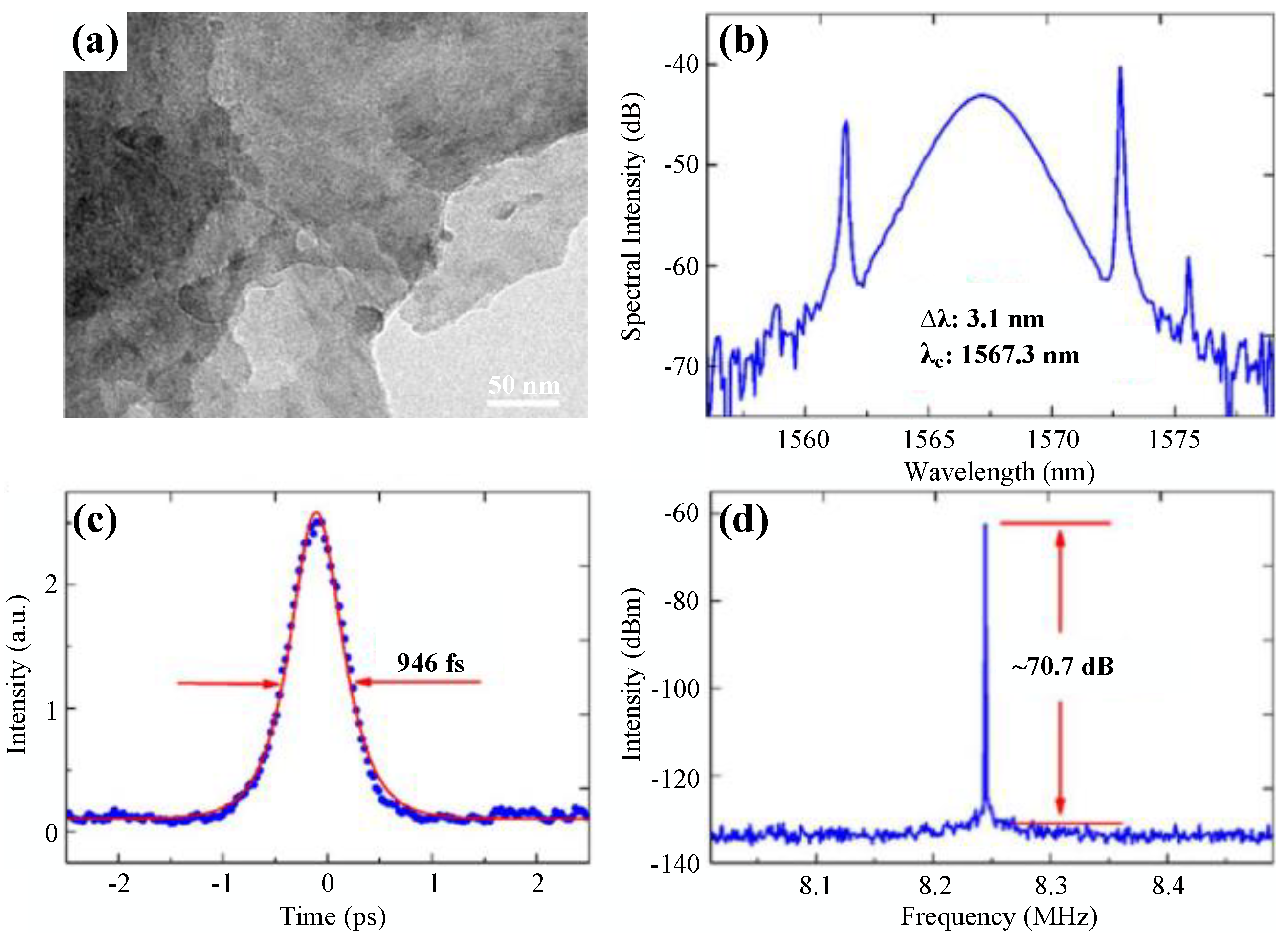
| WS/MoS/WS | MSD | Er | 1562.66 | 296 f | 36.46 M | 0.686 | 25 | 90.3 | [147] | |
| BiTe/Graphene | Solvothermal synthesis | Nd:YAG | 1980 | 238 n–1.22 | 46–108 k | 21.7 | 2340 | – | [344] | |
| MoS/Graphene | HI/E | Er:YSGG | 2797 | 355 n | 126 k | 0.889 | 112 | – | – | [346] |
4. Perspectives
5. Conclusions
Author Contributions
Funding
Institutional Review Board Statement
Informed Consent Statement
Data Availability Statement
Conflicts of Interest
References
- Martin, C.R. Nanomaterials: A membrane-based synthetic approach. Science 1994, 266, 1961–1966. [Google Scholar] [CrossRef]
- Gleiter, H. Nanostructured materials: Basic concepts and microstructure. Acta Mater. 2000, 48, 1–29. [Google Scholar] [CrossRef] [Green Version]
- Gajewicz, A.; Cronin, M.T.D.; Rasulev, B.; Leszczynski, J.; Puzyn, T. Novel approach for efficient predictions properties of large pool of nanomaterials based on limited set of species: Nano-read-across. Nanotechnology 2015, 26, 015701. [Google Scholar] [CrossRef]
- Salata, O. Applications of nanoparticles in biology and medicine. J. Nanobiotechnol. 2004, 2, 3. [Google Scholar] [CrossRef] [PubMed] [Green Version]
- Kumar, C.S.S.R.; Mohammad, F. Magnetic nanomaterials for hyperthermia-based therapy and controlled drug delivery. Adv. Drug Deliv. Rev. 2011, 63, 789–808. [Google Scholar] [CrossRef] [Green Version]
- Langhammer, C.; Larsson, E.M.; Kasemo, B.; Zoric, I. Indirect nanoplasmonic sensing: Ultrasensitive experimental platform for nanomaterials science and optical nanocalorimetry. Nano Lett. 2010, 10, 3529–3538. [Google Scholar] [CrossRef] [PubMed]
- Leonard, F.; Talin, A.A. Electrical contacts to one- and two-dimensional nanomaterials. Nat. Nanotechnol. 2011, 6, 773–783. [Google Scholar] [CrossRef] [PubMed]
- Goldstein, R.V.; Morozov, N.F. Mechanics of deformation and fracture of nanomaterials and nanotechnology. Phys. Mesomech. 2007, 10, 235–246. [Google Scholar] [CrossRef]
- Chen, W.Y.; Wang, Y.Z.; Kuo, S.W.; Huang, C.F.; Tung, P.H.; Chang, F.C. Thermal and dielectric properties and curing kinetics of nanomaterials formed from poss-epoxy and meta-phenylenediamine. Polymer 2004, 45, 6897–6908. [Google Scholar] [CrossRef]
- Huang, X.; Tan, C.L.; Yin, Z.Y.; Zhang, H. 25th anniversary article: Hybrid nanostructures based on two-dimensional nanomaterials. Adv. Mater. 2014, 26, 2185–2204. [Google Scholar] [CrossRef]
- You, J.; Bongu, S.; Bao, Q.; Panoiu, N. Nonlinear optical properties and applications of 2D materials: Theoretical and experimental aspects. Nanophotonics 2019, 8, 63–97. [Google Scholar] [CrossRef]
- Yu, S.L.; Wu, X.Q.; Wang, Y.P.; Guo, X.; Tong, L.M. 2D Materials for Optical Modulation: Challenges and Opportunities. Adv. Mater. 2017, 29, 1606128. [Google Scholar] [CrossRef] [PubMed]
- Woodward, R.I.; Kelleher, E.J.R. 2D saturable absorbers for fibre lasers. Appl. Sci. 2015, 5, 1440–1456. [Google Scholar] [CrossRef] [Green Version]
- Liu, X.; Guo, Q.; Qiu, J. Emerging low-dimensional materials for nonlinear optics and ultrafast photonics. Adv. Mater. 2017, 29, 1605886. [Google Scholar] [CrossRef] [PubMed]
- Wang, J.; Wang, X.; Lei, J.; Ma, M.; Wang, C.; Ge, Y.; Wei, Z. Recent advances in mode-locked fiber lasers based on two-dimensional materials. Nanophotonics 2020, 9, 2315–2340. [Google Scholar] [CrossRef]
- Demaria, A.J.; Glenn, W.H.; Brienza, M.J.; Mack, M.E. Picosecond laser pulses. Proc. IEEE 1969, 57, 2–25. [Google Scholar] [CrossRef]
- Hargrove, L.; Fork, R.L.; Pollack, M. Locking of He–Ne laser modes induced by synchronous intracavity modulation. Appl. Phys. Lett. 1964, 5, 4–5. [Google Scholar] [CrossRef]
- Mocker, H.W.; Collins, R.J. Mode competition and self-locking effects in a Q-switching ruby laser. Appl. Phys. Lett. 1965, 7, 270–273. [Google Scholar] [CrossRef]
- Matsas, V.; Newson, T.; Richardson, D.; Payne, D. Self-starting passively mode-locked fibre ring soliton laser exploiting nonlinear polarisation rotation. Electron. Lett. 1992, 28, 1391–1393. [Google Scholar] [CrossRef] [Green Version]
- Zhang, Z.; Sang, M.; Ye, Z.; Nie, Y. Passively Q-switched erbium-doped fiber laser based on nonlinear polarization rotation. Microw. Opt. Technol. Lett. 2008, 50, 694–696. [Google Scholar] [CrossRef]
- Doran, N.J.; Wood, D. Nonlinear-optical loop mirror. Opt. Lett. 1988, 13, 56–58. [Google Scholar] [CrossRef]
- Barnett, B.C.; Rahman, L.; Islam, M.N.; Chen, Y.C.; Bhattacharya, P.; Riha, W.; Reddy, K.V.; Howe, A.T.; Stair, K.A.; Iwamura, H.; et al. High-power erbium-doped fiber laser mode locked by a semiconductor saturable absorber. Opt. Lett. 1995, 20, 471–473. [Google Scholar] [CrossRef] [PubMed]
- Paschotta, R.; Häring, R.; Gini, E.; Melchior, H.; Keller, U.; Offerhaus, H.L.; Richardson, D.J. Passively Q-switched 0.1-mJ fiber laser system at 1.53 μm. Opt. Lett. 1999, 24, 388–390. [Google Scholar] [CrossRef] [PubMed]
- Okhotnikov, O.; Grudinin, A.; Pessa, M. Ultra-fast fibre laser systems based on SESAM technology: New horizons and applications. New J. Phys. 2004, 6, 177. [Google Scholar] [CrossRef]
- Wang, S.; Wang, W.H.; Lu, J.P.; Ni, Z.H. Chemical vapor deposition growth of large-areas two dimensional materials: Approaches and mechanisms. Acta Phys. Sin. 2021, 70, 026802. [Google Scholar] [CrossRef]
- Fu, B.; Popa, D.; Zhao, Z.; Hussain, S.A.; Flahaut, E.; Hasan, T.; Soavi, G.; Ferrari, A.C. Wavelength tunable soliton rains in a nanotube-mode locked Tm-doped fiber laser. Appl. Phys. Lett. 2018, 113, 193102. [Google Scholar] [CrossRef] [Green Version]
- Set, S.; Yaguchi, H.; Tanaka, Y.; Jablonski, M.; Sakakibara, Y.; Rozhin, A.; Tokumoto, M.; Kataura, H.; Achiba, Y.; Kikuchi, K. Mode-locked fiber lasers based on a saturable absorber incorporating carbon nanotubes. In Proceedings of the Optical Fiber Communication Conference, Optical Society of America, Atlanta, GA, USA, 28 March 2003; p. PD44. [Google Scholar] [CrossRef]
- Yao, J.D.; Zheng, Z.Q.; Yang, G.W. Production of large-area 2D materials for high-performance photodetectors by pulsed-laser deposition. Prog. Mater. Sci. 2019, 106, 100573. [Google Scholar] [CrossRef]
- Duan, W.; Nie, H.; Sun, X.; Zhang, B.; He, G.; Yang, Q.; Xia, H.; Wang, R.; Zhan, J.; He, J. Passively Q-switched mid-infrared laser pulse generation with gold nanospheres as a saturable absorber. Opt. Lett. 2018, 43, 1179–1182. [Google Scholar] [CrossRef]
- Yuan, J.; Bai, X.; Fan, D.; Gu, J.; Wang, S.; Zeng, X. Passively mode-locked erbium-doped fiber laser using gold-nanosphere based on double cladding fiber as saturable absorber. In Proceedings of the 2015 11th Conference on Lasers and Electro-Optics Pacific Rim (CLEO-PR), Busan, Korea, 24–28 August 2015; Volume 2, p. 7375961. [Google Scholar] [CrossRef]
- Meng, Y.; Zhu, C.; Li, Y.; Yuan, X.; Xiu, F.; Shi, Y.; Xu, Y.; Wang, F. Three-dimensional Dirac semimetal thin-film absorber for broadband pulse generation in the near-infrared. Opt. Lett. 2018, 43, 1503–1506. [Google Scholar] [CrossRef]
- Sun, Y.; Meng, Y.; Jiang, H.; Qin, S.; Yang, Y.; Xiu, F.; Shi, Y.; Zhu, S.; Wang, F. Dirac semimetal saturable absorber with actively tunable modulation depth. Opt. Lett. 2019, 44, 582–585. [Google Scholar] [CrossRef]
- Zhao, Q.Z.; Qiu, J.R.; Jiang, X.W.; Zhao, C.J.; Zhu, C.S. Controllable precipitation and dissolution of silver nanoparticles in ultrafast laser pulses irradiated Ag+-doped phosphate glass. Opt. Express 2004, 12, 4035–4040. [Google Scholar] [CrossRef]
- Lin, Y.H.; Chi, Y.C.; Lin, G.R. Nanoscale charcoal powder induced saturable absorption and mode-locking of a low-gain erbium-doped fiber-ring laser. Laser Phys. Lett. 2013, 10, 055105. [Google Scholar] [CrossRef]
- Li, W.; Hu, H.; Zhang, X.; Zhao, S.; Fu, K.; Dutta, N.K. High-speed ultrashort pulse fiber ring laser using charcoal nanoparticles. Appl. Opt. 2016, 55, 2149–2154. [Google Scholar] [CrossRef]
- Lin, Y.H.; Lo, J.Y.; Tseng, W.H.; Wu, C.I.; Lin, G.R. Self-amplitude and self-phase modulation of the charcoal mode-locked erbium-doped fiber lasers. Opt. Express 2013, 21, 25184–25196. [Google Scholar] [CrossRef]
- Guinea, F.; Katnelson, M.I.; Wehling, T.O. Two-dimensional materials: Electronic structure and many-body effects. Ann. Phys. 2014, 526, A81–A82. [Google Scholar] [CrossRef]
- Novoselov, K.S.; Geim, A.K.; Morozov, S.V.; Jiang, D.; Zhang, Y.; Dubonos, S.V.; Grigorieva, I.V.; Firsov, A.A. Electric field effect in atomically thin carbon films. Science 2004, 306, 666–669. [Google Scholar] [CrossRef] [PubMed] [Green Version]
- Luo, Z.; Zhou, M.; Weng, J.; Huang, G.; Xu, H.; Ye, C.; Cai, Z. Graphene-based passively Q-switched dual-wavelength erbium-doped fiber laser. Opt. Lett. 2010, 35, 3709–3711. [Google Scholar] [CrossRef] [Green Version]
- Hasan, T.; Sun, Z.; Wang, F.; Bonaccorso, F.; Tan, P.H.; Rozhin, A.G.; Ferrari, A.C. Nanotube polymer composites for ultrafast photonics. Adv. Mater. 2009, 21, 3874–3899. [Google Scholar] [CrossRef]
- Bao, Q.; Zhang, H.; Wang, Y.; Ni, Z.; Yan, Y.; Shen, Z.X.; Loh, K.P.; Tang, D.Y. Atomic-layer graphene as a saturable absorber for ultrafast pulsed lasers. Adv. Funct. Mater. 2009, 19, 3077–3083. [Google Scholar] [CrossRef]
- Wang, G.; Baker-Murray, A.A.; Blau, W.J. Saturable absorption in 2D nanomaterials and related photonic devices. Laser Photonics Rev. 2019, 13, 1800282. [Google Scholar] [CrossRef]
- Ma, C.; Wang, C.; Gao, B.; Adams, J.; Wu, G.; Zhang, H. Recent progress in ultrafast lasers based on 2D materials as a saturable absorber. Appl. Phys. Rev. 2019, 6, 041304. [Google Scholar] [CrossRef]
- Fu, B.; Gui, L.; Zhang, W.; Xiao, X.; Zhu, H.; Yang, C. Passive harmonic mode locking in erbium-doped fiber laser with graphene saturable absorber. Opt. Commun. 2013, 286, 304–308. [Google Scholar] [CrossRef]
- Bernard, F.; Zhang, H.; Gorza, S.P.; Emplit, P. Towards mode-locked fiber laser using topological insulators. In Proceedings of the Advanced Photonics Congress, Optical Society of America, Colorado Springs, CO, USA, 17–21 June 2012; OSA Technical Digest (online). p. NTh1A.5. [Google Scholar] [CrossRef] [Green Version]
- Pinghua, T.; Xiaoqi, Z.; Chujun, Z.; Yong, W.; Han, Z.; Deyuan, S.; Shuangchun, W.; Dingyuan, T.; Dianyuan, F. Topological insulator: Bi2Te3 saturable absorber for the passive Q-switching operation of an in-band pumped 1645-nm Er:YAG ceramic laser. IEEE Photonics J. 2013, 5, 1500707. [Google Scholar] [CrossRef]
- Zhang, H.; Lu, S.B.; Zheng, J.; Du, J.; Wen, S.C.; Tang, D.Y.; Loh, K.P. Molybdenum disulfide (MoS2) as a broadband saturable absorber for ultra-fast photonics. Opt. Express 2014, 22, 7249–7260. [Google Scholar] [CrossRef] [PubMed]
- Woodward, R.I.; Kelleher, E.J.R.; Runcorn, T.H.; Popov, S.V.; Torrisi, F.; Howe, R.C.T.; Hasan, T. Q-switched fiber laser with MoS2 saturable absorber. In Proceedings of the CLEO: Science and Innovations, Optical Society of America, San Jose, CA, USA, 8–13 June 2014; p. SM3H.6. [Google Scholar] [CrossRef]
- Chen, Y.; Jiang, G.; Chen, S.; Guo, Z.; Yu, X.; Zhao, C.; Zhang, H.; Bao, Q.; Wen, S.; Tang, D.; et al. Mechanically exfoliated black phosphorus as a new saturable absorber for both Q-switching and Mode-locking laser operation. Opt. Express 2015, 23, 12823–12833. [Google Scholar] [CrossRef] [PubMed] [Green Version]
- Li, D.; Jussila, H.; Karvonen, L.; Ye, G.; Lipsanen, H.; Chen, X.; Sun, Z. Polarization and thickness dependent absorption properties of black phosphorus: New saturable absorber for ultrafast pulse generation. Sci. Rep. 2015, 5, 15899. [Google Scholar] [CrossRef] [PubMed] [Green Version]
- Fu, B.; Sun, J.; Wang, C.; Shang, C.; Xu, L.; Li, J.; Zhang, H. MXenes: Synthesis, optical properties, and applications in ultrafast photonics. Small 2021, 17, 2006054. [Google Scholar] [CrossRef] [PubMed]
- Lu, L.; Liang, Z.M.; Wu, L.M.; Chen, Y.X.; Song, Y.F.; Dhanabalan, S.C.; Ponraj, J.S.; Dong, B.Q.; Xiang, Y.J.; Xing, F.; et al. Few-layer bismuthene: Sonochemical exfoliation, nonlinear optics and applications for ultrafast photonics with enhanced stability. Laser Photonics Rev. 2018, 12, 1700221. [Google Scholar] [CrossRef]
- Pumera, M.; Sofer, Z. 2D monoelemental arsenene, antimonene, and bismuthene: Beyond black phosphorus. Adv. Mater. 2017, 29, 1605299. [Google Scholar] [CrossRef]
- Zhang, Y.; Lu, D.; Yu, H.; Zhang, H. Low-dimensional saturable absorbers in the visible spectral region. Adv. Opt. Mater. 2019, 7, 1800886. [Google Scholar] [CrossRef] [Green Version]
- Fu, B.; Hua, Y.; Xiao, X.; Zhu, H.; Sun, Z.; Yang, C. Broadband graphene saturable absorber for pulsed fiber lasers at 1, 1.5, and 2 μm. IEEE J. Sel. Top. Quantum Electron. 2014, 20, 411–415. [Google Scholar] [CrossRef]
- Yi, J.; Du, L.; Li, J.; Yang, L.; Hu, L.; Huang, S.; Dong, Y.; Miao, L.; Wen, S.; Mochalin, V.N.; et al. Unleashing the potential of Ti2CTx MXene as a pulse modulator for mid-infrared fiber lasers. 2D Mater. 2019, 6, 045038. [Google Scholar] [CrossRef]
- Loiko, P.; Bora, T.; Serres, J.M.; Mateos, X.; Yu, H.H.; Baranov, A.; Aguilo, M.; Diaz, F.; Griebner, U.; Petrov, V.; et al. Oriented ZnO nanorods: A novel saturable absorber for lasers at 1–2 μm. In Proceedings of the European Conference on Lasers and Electro-Optics, Optical Society of America, Munich, Germany, 25–29 June 2017; p. CE_7_4. [Google Scholar] [CrossRef]
- Baranov, A.I.; Myasnikov, D.V.; Protasenya, D.V.; Demkin, A.S.; Gapontsev, V.P. High power ultrashort fiber laser system at 1.55 um. In Proceedings of the 2016 International Conference Laser Optics, Institute of Electrical and Electronics Engineers Inc., St. Petersburg, Russia, 27 June–1 July 2016; p. 7549939. [Google Scholar] [CrossRef]
- Cho, W.B.; Schmidt, A.; Yim, J.H.; Choi, S.Y.; Lee, S.; Rotermund, F.; Griebner, U.; Steinmeyer, G.; Petrov, V.; Mateos, X.; et al. Passive mode-locking of a Tm-doped bulk laser near 2 µm using a carbon nanotube saturable absorber. Opt. Express 2009, 17, 11007–11012. [Google Scholar] [CrossRef] [PubMed]
- Rotermund, F.; Petrov, V.; Noack, F.; Wittmann, M.; Korn, G. Laser-diode-seeded operation of a femtosecond optical parametric amplifier with MgO: LiNbO3 and generation of 5-cycle pulses near 3 µm. J. Opt. Soc. Am. B 1999, 16, 1539–1545. [Google Scholar] [CrossRef]
- Hernandez, Y.; Nicolosi, V.; Lotya, M.; Blighe, F.M.; Sun, Z.Y.; De, S.; McGovern, I.T.; Holland, B.; Byrne, M.; Gun’ko, Y.K.; et al. High-yield production of graphene by liquid-phase exfoliation of graphite. Nat. Nanotechnol. 2008, 3, 563–568. [Google Scholar] [CrossRef] [PubMed] [Green Version]
- Serna, M.I.; Yoo, S.H.; Moreno, S.; Xi, Y.; Oviedo, J.P.; Choi, H.; Alshareef, H.N.; Kim, M.J.; Minary-Jolandan, M.; Quevedo-Lopez, M.A. Large-area deposition of MoS2 by pulsed laser deposition with in situ thickness control. ACS Nano 2016, 10, 6054–6061. [Google Scholar] [CrossRef] [PubMed] [Green Version]
- He, J.; Tao, L.; Zhang, H.; Zhou, B.; Li, J. Emerging 2D materials beyond graphene for ultrashort pulse generation in fiber lasers. Nanoscale 2019, 11, 2577–2593. [Google Scholar] [CrossRef]
- Liu, H.; Neal, A.T.; Zhu, Z.; Luo, Z.; Xu, X.F.; Tomanek, D.; Ye, P.D. Phosphorene: An unexplored 2D semiconductor with a high hole mobility. ACS Nano 2014, 8, 4033–4041. [Google Scholar] [CrossRef] [Green Version]
- Yin, Z.Y.; Li, H.; Li, H.; Jiang, L.; Shi, Y.M.; Sun, Y.H.; Lu, G.; Zhang, Q.; Chen, X.D.; Zhang, H. Single-Layer MoS2 Phototransistors. ACS Nano 2012, 6, 74–80. [Google Scholar] [CrossRef] [Green Version]
- Teweldebrhan, D.; Goyal, V.; Balandin, A.A. Exfoliation and characterization of bismuth telluride atomic quintuples and quasi-two-dimensional crystals. Nano Lett. 2010, 10, 1209–1218. [Google Scholar] [CrossRef]
- Li, H.; Lu, G.; Wang, Y.L.; Yin, Z.Y.; Cong, C.X.; He, Q.Y.; Wang, L.; Ding, F.; Yu, T.; Zhang, H. Mechanical exfoliation and characterization of single- and few-layer nanosheets of WSe2, TaS2, and TaSe2. Small 2013, 9, 1974–1981. [Google Scholar] [CrossRef]
- Shahil, K.M.F.; Hossain, M.Z.; Goyal, V.; Balandin, A.A. Micro-Raman spectroscopy of mechanically exfoliated few-quintuple layers of Bi2Te3, Bi2Se3, and Sb2Te3 materials. J. Appl. Phys. 2012, 111, 054305. [Google Scholar] [CrossRef] [Green Version]
- Gkountaras, A.; Kim, Y.; Coraux, J.; Bouchiat, V.; Lisi, S.; Barsoum, M.W.; Ouisse, T. Mechanical exfoliation of select MAX phases and Mo4Ce4Al7C3 single crystals to produce MAXenes. Small 2020, 16, 1905784. [Google Scholar] [CrossRef] [PubMed]
- Fu, B.; Sun, J.; Wang, G.; Shang, C.; Ma, Y.; Ma, J.; Xu, L.; Scardaci, V. Solution-processed two-dimensional materials for ultrafast fiber lasers (invited). Nanophotonics 2020, 9, 2169–2189. [Google Scholar] [CrossRef] [Green Version]
- Joensen, P.; Frindt, R.; Morrison, S.R. Single-layer MoS2. Mater. Res. Bull. 1986, 21, 457–461. [Google Scholar] [CrossRef]
- Yang, D.; Frindt, R.F. Li-intercalation and exfoliation of WS2. J. Phys. Chem. Solids 1996, 57, 1113–1116. [Google Scholar] [CrossRef]
- Eda, G.; Yamaguchi, H.; Voiry, D.; Fujita, T.; Chen, M.W.; Chhowalla, M. Photoluminescence from Chemically Exfoliated MoS2. Nano Lett. 2011, 11, 5111–5116. [Google Scholar] [CrossRef] [PubMed]
- Ren, L.; Qi, X.; Liu, Y.D.; Hao, G.L.; Huang, Z.Y.; Zou, X.H.; Yang, L.W.; Li, J.; Zhong, J.X. Large-scale production of ultrathin topological insulator bismuth telluride nanosheets by a hydrothermal intercalation and exfoliation route. J. Mater. Chem. 2012, 22, 4921–4926. [Google Scholar] [CrossRef]
- Meng, Y.C.; Semaan, G.; Salhi, M.; Niang, A.; Guesmi, K.; Luo, Z.C.; Sanchez, F. High power L-band mode-locked fiber laser based on topological insulator saturable absorber. Opt. Express 2015, 23, 23053–23058. [Google Scholar] [CrossRef]
- Gao, L.; Huang, W.; Zhang, J.D.; Zhu, T.; Zhang, H.; Zhao, C.J.; Zhang, W.; Zhang, H. Q-switched mode-locked erbium-doped fiber laser based on topological insulator Bi2Se3 deposited fiber taper. Appl. Opt. 2014, 53, 5117–5122. [Google Scholar] [CrossRef]
- Lin, Y.H.; Yang, C.Y.; Liou, J.H.; Yu, C.P.; Lin, G.R. Using graphene nano-particle embedded in photonic crystal fiber for evanescent wave mode-locking of fiber laser. Opt. Express 2013, 21, 16763–16776. [Google Scholar] [CrossRef]
- Wang, T.; Zhang, W.C.; Shi, X.Y.; Wang, J.; Ding, X.G.; Zhang, K.; Peng, J.S.; Wu, J.; Zhou, P. Black phosphorus-enabled harmonic mode locking of dark pulses in a Yb-doped fiber laser. Laser Phys. Lett. 2019, 16, 85102. [Google Scholar] [CrossRef]
- Song, H.Q.; Wang, Q.; Zhang, Y.F.; Li, L. Mode-locked ytterbium-doped all-fiber lasers based on few-layer black phosphorus saturable absorbers. Opt. Commun. 2017, 394, 157–160. [Google Scholar] [CrossRef]
- Li, J.F.; Luo, H.Y.; Zhai, B.; Lu, R.G.; Guo, Z.N.; Zhang, H.; Liu, Y. Black phosphorus: A two-dimension saturable absorption material for mid-infrared Q-switched and mode-locked fiber lasers. Sci. Rep. 2016, 6, 30361. [Google Scholar] [CrossRef] [Green Version]
- Qin, Z.; Xie, G.; Zhang, H.; Zhao, C.; Yuan, P.; Wen, S.; Qian, L. Black phosphorus as saturable absorber for the Q-switched Er:ZBLAN fiber laser at 2.8 µm. Opt. Express 2015, 23, 24713–24718. [Google Scholar] [CrossRef] [PubMed]
- Lu, S.B.; Miao, L.L.; Guo, Z.N.; Qi, X.; Zhao, C.J.; Zhang, H.; Wen, S.C.; Tang, D.Y.; Fan, D.Y. Broadband nonlinear optical response in multi-layer black phosphorus: An emerging infrared and mid-infrared optical material. Opt. Express 2015, 23, 11183–11194. [Google Scholar] [CrossRef]
- Coleman, J.N.; Lotya, M.; O’Neill, A.; Bergin, S.D.; King, P.J.; Khan, U.; Young, K.; Gaucher, A.; De, S.; Smith, R.J.; et al. Two-dimensional nanosheets produced by liquid exfoliation of layered materials. Science 2011, 331, 568–571. [Google Scholar] [CrossRef] [PubMed] [Green Version]
- Smith, R.J.; King, P.J.; Lotya, M.; Wirtz, C.; Khan, U.; De, S.; O’Neill, A.; Duesberg, G.S.; Grunlan, J.C.; Moriarty, G.; et al. Large-scale exfoliation of inorganic layered compounds in aqueous surfactant solutions. Adv. Mater. 2011, 23, 3944–3948. [Google Scholar] [CrossRef]
- Liu, H.; Zheng, X.W.; Liu, M.; Zhao, N.; Luo, A.P.; Luo, Z.C.; Xu, W.C.; Zhang, H.; Zhao, C.J.; Wen, S.C. Femtosecond pulse generation from a topological insulator mode-locked fiber laser. Opt. Express 2014, 22, 6868–6873. [Google Scholar] [CrossRef] [PubMed] [Green Version]
- Chen, Y.; Zhao, C.; Huang, H.; Chen, S.; Tang, P.; Wang, Z.; Lu, S.; Zhang, H.; Wen, S.; Tang, D. Self-assembled topological insulator: Bi2Se3 membrane as a passive Q-switcher in an erbium-doped fiber laser. J. Light. Technol. 2013, 31, 2857–2863. [Google Scholar] [CrossRef]
- Zhao, C.; Zou, Y.; Chen, Y.; Wang, Z.; Lu, S.; Zhang, H.; Wen, S.; Tang, D. Wavelength-tunable picosecond soliton fiber laser with Topological Insulator: Bi2Se3 as a mode locker. Opt. Express 2012, 20, 27888–27895. [Google Scholar] [CrossRef] [PubMed]
- Dou, Z.Y.; Song, Y.R.; Tian, J.R.; Liu, J.H.; Yu, Z.H.; Fang, X.H. Mode-locked ytterbium-doped fiber laser based on topological insulator: Bi2Se3. Opt. Express 2014, 22, 24055–24061. [Google Scholar] [CrossRef] [PubMed]
- Sun, L.P.; Lin, Z.Q.; Peng, J.; Weng, J.; Huang, Y.Z.; Luo, Z.Q. Preparation of few-layer bismuth selenide by liquid-phase-exfoliation and its optical absorption properties. Sci. Rep. 2014, 4, 4794. [Google Scholar] [CrossRef] [Green Version]
- Bonaccorso, F.; Bartolotta, A.; Coleman, J.N.; Backes, C. 2D-crystal-based functional inks. Adv. Mater. 2016, 28, 6136–6166. [Google Scholar] [CrossRef] [PubMed]
- Coleman, J.N. Liquid exfoliation of defect-free graphene. Acc. Chem. Res. 2013, 46, 14–22. [Google Scholar] [CrossRef]
- Green, A.A.; Hersam, M.C. Solution phase production of graphene with controlled thickness via density differentiation. Nano Lett. 2009, 9, 4031–4036. [Google Scholar] [CrossRef]
- Kang, J.; Wood, J.D.; Wells, S.A.; Lee, J.H.; Liu, X.L.; Chen, K.S.; Hersam, M.C. Solvent exfoliation of electronic-grade, two-dimensional black phosphorus. ACS Nano 2015, 9, 3596–3604. [Google Scholar] [CrossRef] [PubMed] [Green Version]
- Nicolosi, V.; Chhowalla, M.; Kanatzidis, M.G.; Strano, M.S.; Coleman, J.N. Liquid exfoliation of layered materials. Science 2013, 340, 1226419. [Google Scholar] [CrossRef] [Green Version]
- Backes, C.; Smith, R.J.; McEvoy, N.; Berner, N.C.; McCloskey, D.; Nerl, H.C.; O’Neill, A.; King, P.J.; Higgins, T.; Hanlon, D.; et al. Edge and confinement effects allow in situ measurement of size and thickness of liquid-exfoliated nanosheets. Nat. Commun. 2014, 5, 4576. [Google Scholar] [CrossRef] [PubMed]
- Hassoun, J.; Bonaccorso, F.; Agostini, M.; Angelucci, M.; Betti, M.G.; Cingolani, R.; Gemmi, M.; Mariani, C.; Panero, S.; Pellegrini, V.; et al. An advanced lithium-ion battery based on a graphene anode and a lithium iron phosphate cathode. Nano Lett. 2014, 14, 4901–4906. [Google Scholar] [CrossRef] [PubMed] [Green Version]
- Knieke, C.; Berger, A.; Voigt, M.; Taylor, R.N.K.; Rohrl, J.; Peukert, W. Scalable production of graphene sheets by mechanical delamination. Carbon 2010, 48, 3196–3204. [Google Scholar] [CrossRef]
- Yao, Y.G.; Lin, Z.Y.; Li, Z.; Song, X.J.; Moon, K.S.; Wong, C.P. Large-scale production of two-dimensional nanosheets. J. Mater. Chem. 2012, 22, 13494–13499. [Google Scholar] [CrossRef]
- Ibrahem, M.A.; Lan, T.W.; Huang, J.K.; Chen, Y.Y.; Wei, K.H.; Li, L.J.; Chu, C.W. High quantity and quality few-layers transition metal disulfide nanosheets from wet-milling exfoliation. RSC Adv. 2013, 3, 13193–13202. [Google Scholar] [CrossRef]
- Paton, K.R.; Varrla, E.; Backes, C.; Smith, R.J.; Khan, U.; O’Neill, A.; Boland, C.; Lotya, M.; Istrate, O.M.; King, P.; et al. Scalable production of large quantities of defect-free few-layer graphene by shear exfoliation in liquids. Nat. Mater. 2014, 13, 624–630. [Google Scholar] [CrossRef]
- Cheng, P.W.; Tang, C.Y.; Wang, X.Y.; Ma, S.N.; Long, H.; Tsang, Y.E.H. Passively Q-switched ytterbium-doped fiber laser based on broadband multilayer platinum ditelluride (PtTe2) saturable absorber. Sci. Rep. 2019, 9, 10106. [Google Scholar] [CrossRef] [Green Version]
- Zhou, K.G.; Mao, N.N.; Wang, H.X.; Peng, Y.; Zhang, H.L. A mixed-solvent strategy for efficient exfoliation of inorganic graphene analogues. Angew. Chem. Int. Ed. 2011, 50, 10839–10842. [Google Scholar] [CrossRef]
- Halim, U.; Zheng, C.R.; Chen, Y.; Lin, Z.Y.; Jiang, S.; Cheng, R.; Huang, Y.; Duan, X.F. A rational design of cosolvent exfoliation of layered materials by directly probing liquid-solid interaction. Nat. Commun. 2013, 4, 2213. [Google Scholar] [CrossRef] [PubMed]
- Lotya, M.; Hernandez, Y.; King, P.J.; Smith, R.J.; Nicolosi, V.; Karlsson, L.S.; Blighe, F.M.; De, S.; Wang, Z.M.; McGovern, I.T.; et al. Liquid phase production of graphene by exfoliation of graphite in surfactant/water solutions. J. Am. Chem. Soc. 2009, 131, 3611–3620. [Google Scholar] [CrossRef] [PubMed] [Green Version]
- Niu, L.Y.; Coleman, J.N.; Zhang, H.; Shin, H.; Chhowalla, M.; Zheng, Z.J. Production of two-dimensional nanomaterials via liquid-based direct exfoliation. Small 2016, 12, 272–293. [Google Scholar] [CrossRef] [PubMed]
- Varrla, E.; Paton, K.R.; Backes, C.; Harvey, A.; Smith, R.J.; McCauley, J.; Coleman, J.N. Turbulence-assisted shear exfoliation of graphene using household detergent and a kitchen blender. Nanoscale 2014, 6, 11810–11819. [Google Scholar] [CrossRef] [Green Version]
- Ciesielski, A.; Samori, P. Graphene via sonication assisted liquid-phase exfoliation. Chem. Soc. Rev. 2014, 43, 381–398. [Google Scholar] [CrossRef]
- Zhu, J.; Kang, J.; Kang, J.M.; Jariwala, D.; Wood, J.D.; Seo, J.W.T.; Chen, K.S.; Marks, T.J.; Hersam, M.C. Solution-processed dielectrics based on thickness-sorted two-dimensional hexagonal boron nitride nanosheets. Nano Lett. 2015, 15, 7029–7036. [Google Scholar] [CrossRef] [PubMed]
- Kang, J.; Seo, J.W.T.; Alducin, D.; Ponce, A.; Yacaman, M.J.; Hersam, M.C. Thickness sorting of two-dimensional transition metal dichalcogenides via copolymer-assisted density gradient ultracentrifugation. Nat. Commun. 2014, 5, 5478. [Google Scholar] [CrossRef]
- May, P.; Khan, U.; Hughes, J.M.; Coleman, J.N. Role of solubility parameters in understanding the steric stabilization of exfoliated two-dimensional nanosheets by adsorbed polymers. J. Phys. Chem. C 2012, 116, 24390–24391. [Google Scholar] [CrossRef]
- Vega-Mayoral, V.; Backes, C.; Hanlon, D.; Khan, U.; Gholamvand, Z.; O’Brien, M.; Duesberg, G.S.; Gadermaier, C.; Coleman, J.N. Photoluminescence from Liquid-Exfoliated WS2 Monomers in Poly(Vinyl Alcohol) Polymer Composites. Adv. Funct. Mater. 2016, 26, 1028–1039. [Google Scholar] [CrossRef]
- Svedberg, T.; Pedersen, K.O. The Ultracentrifuge; Oxford University Press: Oxford, UK, 1940. [Google Scholar]
- O’Neill, A.; Khan, U.; Coleman, J.N. Preparation of high concentration dispersions of exfoliated MoS2 with increased flake size. Chem. Mater. 2012, 24, 2414–2421. [Google Scholar] [CrossRef]
- Williams, J.; Van Holde, K.E.; Baldwin, R.L.; Fujita, H. The theory of sedimentation analysis. Chem. Rev. 1958, 58, 715–744. [Google Scholar] [CrossRef]
- Ifft, J.B.; Vinograd, J. The buoyant behavior of bovine serum mercaptalbumin in salt solutions at equilibrium in the ultracentrifuge. II. net hydration, ion binding, and solvated molecular weight in various salt solutions. J. Phys. Chem. 1966, 70, 2814–2822. [Google Scholar] [CrossRef]
- Naguib, M.; Kurtoglu, M.; Presser, V.; Lu, J.; Niu, J.J.; Heon, M.; Hultman, L.; Gogotsi, Y.; Barsoum, M.W. Two-dimensional nanocrystals produced by exfoliation of Ti3AlC2. Adv. Mater. 2011, 23, 4248–4253. [Google Scholar] [CrossRef] [Green Version]
- Naguib, M.; Mashtalir, O.; Carle, J.; Presser, V.; Lu, J.; Hultman, L.; Gogotsi, Y.; Barsoum, M.W. Two-dimensional transition metal carbides. ACS Nano 2012, 6, 1322–1331. [Google Scholar] [CrossRef]
- Peng, C.; Wei, P.; Chen, X.; Zhang, Y.L.; Zhu, F.; Cao, Y.H.; Wang, H.J.; Yu, H.; Peng, F. A hydrothermal etching route to synthesis of 2D MXene (Ti3C2, Nb2C): Enhanced exfoliation and improved adsorption performance. Ceram. Int. 2018, 44, 18886–18893. [Google Scholar] [CrossRef]
- Naguib, M.; Halim, J.; Lu, J.; Cook, K.M.; Hultman, L.; Gogotsi, Y.; Barsoum, M.W. New two-dimensional niobium and vanadium carbides as promising materials for li-ion batteries. J. Am. Chem. Soc. 2013, 135, 15966–15969. [Google Scholar] [CrossRef] [PubMed]
- Chang, F.Y.; Li, C.S.; Yang, J.; Tang, H.; Xue, M.Q. Synthesis of a new graphene-like transition metal carbide by de-intercalating Ti3AlC2. Mater. Lett. 2013, 109, 295–298. [Google Scholar] [CrossRef]
- Anasori, B.; Shi, C.Y.; Moon, E.J.; Xie, Y.; Voigt, C.A.; Kent, P.R.C.; May, S.J.; Billinge, S.J.L.; Barsoum, M.W.; Gogotsi, Y. Control of electronic properties of 2D carbides (MXenes) by manipulating their transition metal layers. Nanoscale Horiz. 2016, 1, 227–234. [Google Scholar] [CrossRef] [PubMed]
- Halim, J.; Lukatskaya, M.R.; Cook, K.M.; Lu, J.; Smith, C.R.; Naslund, L.A.; May, S.J.; Hultman, L.; Gogotsi, Y.; Eklund, P.; et al. Transparent conductive two-dimensional titanium carbide epitaxial thin films. Chem. Mater. 2014, 26, 2374–2381. [Google Scholar] [CrossRef] [PubMed]
- Ghidiu, M.; Lukatskaya, M.R.; Zhao, M.Q.; Gogotsi, Y.; Barsoum, M.W. Conductive two-dimensional titanium carbide ’clay’ with high volumetric capacitance. Nature 2014, 516, 78–81. [Google Scholar] [CrossRef]
- Ying, G.B.; Dillon, A.D.; Fafarman, A.T.; Barsoum, M.W. Transparent, conductive solution processed spincast 2D Ti2CTx (MXene) films. Mater. Res. Lett. 2017, 5, 391–398. [Google Scholar] [CrossRef] [Green Version]
- Liu, F.F.; Zhou, A.G.; Chen, J.F.; Jin, J.; Zhou, W.J.; Wang, L.B.; Hu, Q.K. Preparation of Ti3C2 and Ti2C MXenes by fluoride salts etching and methane adsorptive properties. Appl. Surf. Sci. 2017, 416, 781–789. [Google Scholar] [CrossRef]
- Du, F.; Tang, H.; Pan, L.M.; Zhang, T.; Lu, H.M.; Xiong, J.; Yang, J.; Zhang, C. Environmental friendly scalable production of colloidal 2D titanium carbonitride MXene with minimized nanosheets restacking for excellent cycle life lithium-ion batteries. Electrochim. Acta 2017, 235, 690–699. [Google Scholar] [CrossRef]
- Castellanos-Gomez, A.; Barkelid, M.; Goossens, A.M.; Calado, V.E.; van der Zant, H.S.J.; Steele, G.A. Laser-thinning of MoS2: On demand generation of a single-layer semiconductor. Nano Lett. 2012, 12, 3187–3192. [Google Scholar] [CrossRef] [Green Version]
- Gu, E.Y.; Wang, Q.Y.; Zhang, Y.W.; Cong, C.X.; Hu, L.G.; Tian, P.F.; Liu, R.; Zhang, S.L.; Qiu, Z.J. A real-time raman spectroscopy study of the dynamics of laser-thinning of MoS2 flakes to monolayers. AIP Adv. 2017, 7, 125329. [Google Scholar] [CrossRef]
- Hu, L.L.; Shan, X.Y.; Wu, Y.L.; Zhao, J.M.; Lu, X.H. Laser thinning and patterning of MoS2 with layer-by-layer precision. Sci. Rep. 2017, 7, 15538. [Google Scholar] [CrossRef] [PubMed]
- Bala, L.; Lacinska, E.M.; Nogajewski, K.; Molas, M.R.; Wysmolek, A.; Potemski, M. Strong photoluminescence fluctuations in laser-thinned few-layer WS2. Acta Phys. Pol. A 2016, 130, 1176–1178. [Google Scholar] [CrossRef]
- Han, G.H.; Chae, S.J.; Kim, E.S.; Gunes, F.; Lee, I.H.; Lee, S.W.; Lee, S.Y.; Lim, S.C.; Jeong, H.K.; Jeong, M.S.; et al. Laser thinning for monolayer graphene formation: Heat sink and interference effect. ACS Nano 2011, 5, 263–268. [Google Scholar] [CrossRef] [PubMed]
- Li, D.W.; Zhou, Y.S.; Huang, X.; Jiang, L.; Silvain, J.F.; Lu, Y.F. In situ imaging and control of layer-by-layer femtosecond laser thinning of graphene. Nanoscale 2015, 7, 3651–3659. [Google Scholar] [CrossRef]
- Lin, Z.; Ye, X.H.; Han, J.P.; Chen, Q.; Fan, P.X.; Zhang, H.J.; Xie, D.; Zhu, H.W.; Zhong, M.L. Precise control of the number of layers of graphene by picosecond laser thinning. Sci. Rep. 2015, 5, 11662. [Google Scholar] [CrossRef] [PubMed]
- Li, X.S.; Cai, W.W.; An, J.H.; Kim, S.; Nah, J.; Yang, D.X.; Piner, R.; Velamakanni, A.; Jung, I.; Tutuc, E.; et al. Large-area synthesis of high-quality and uniform graphene films on copper foils. Science 2009, 324, 1312–1314. [Google Scholar] [CrossRef] [PubMed] [Green Version]
- Khazaeinezhad, R.; Kassani, S.H.; Jeong, H.; Yeom, D.I.; Oh, K. Femtosecond soliton pulse generation using evanescent field interaction through Tungsten disulfide (WS2) film. J. Light. Technol. 2015, 33, 3550–3557. [Google Scholar] [CrossRef]
- Yu, Q.K.; Lian, J.; Siriponglert, S.; Li, H.; Chen, Y.P.; Pei, S.S. Graphene segregated on Ni surfaces and transferred to insulators. Appl. Phys. Lett. 2008, 93, 113103. [Google Scholar] [CrossRef] [Green Version]
- Chang, Y.H.; Zhang, W.; Zhu, Y.; Han, Y.; Pu, J.; Chang, J.K.; Hsu, W.T.; Huang, J.K.; Hsu, C.L.; Chiu, M.H.; et al. Monolayer MoSe2 grown by chemical vapor deposition for fast photodetection. ACS Nano 2014, 8, 8582–8590. [Google Scholar] [CrossRef] [Green Version]
- Xu, C.; Wang, L.B.; Liu, Z.B.; Chen, L.; Guo, J.K.; Kang, N.; Ma, X.L.; Cheng, H.M.; Ren, W.C. Large-area high-quality 2D ultrathin Mo2C superconducting crystals. Nat. Mater. 2015, 14, 1135–1141. [Google Scholar] [CrossRef] [PubMed]
- Liu, W.J.; Liu, M.L.; Yin, J.D.; Chen, H.; Lu, W.; Fang, S.B.; Teng, H.; Lei, M.; Yan, P.G.; Wei, Z.Y. Tungsten diselenide for all-fiber lasers with the chemical vapor deposition method. Nanoscale 2018, 10, 7971–7977. [Google Scholar] [CrossRef] [PubMed]
- Sutter, P.; Lahiri, J.; Zahl, P.; Wang, B.; Sutter, E. Scalable synthesis of uniform few-layer hexagonal boron nitride dielectric films. Nano Lett. 2013, 13, 276–281. [Google Scholar] [CrossRef] [PubMed]
- Ullah, F.; Nguyen, T.K.; Le, C.T.; Kim, Y.S. Pulsed laser deposition assisted grown continuous monolayer MoSe2. Crystengcomm 2016, 18, 6992–6996. [Google Scholar] [CrossRef]
- Shi, Y.M.; Hamsen, C.; Jia, X.T.; Kim, K.K.; Reina, A.; Hofmann, M.; Hsu, A.L.; Zhang, K.; Li, H.N.; Juang, Z.Y.; et al. Synthesis of few-layer hexagonal boron nitride thin film by chemical vapor deposition. Nano Lett. 2010, 10, 4134–4139. [Google Scholar] [CrossRef] [PubMed]
- Zhang, C.; Liu, M.; Man, B.Y.; Jiang, S.Z.; Yang, C.; Chen, C.S.; Feng, D.J.; Bi, D.; Liu, F.Y.; Qiu, H.W.; et al. Facile fabrication of graphene-topological insulator Bi2Se3 hybrid Dirac materials via chemical vapor deposition in Se-rich conditions. Crystengcomm 2014, 16, 8941–8945. [Google Scholar] [CrossRef]
- Gu, Y.; Cai, H.; Dong, J.; Yu, Y.; Hoffman, A.N.; Liu, C.; Oyedele, A.D.; Lin, Y.C.; Ge, Z.; Puretzky, A.A.; et al. Two-dimensional palladium diselenide with strong in-plane optical anisotropy and high mobility grown by chemical vapor deposition. Adv. Mater. 2020, 32, e1906238. [Google Scholar] [CrossRef]
- Cai, Z.Y.; Liu, B.L.; Zou, X.L.; Cheng, H.M. Chemical vapor deposition growth and applications of two-dimensional materials and their heterostructures. Chem. Rev. 2018, 118, 6091–6133. [Google Scholar] [CrossRef]
- Tang, L.; Li, T.; Luo, Y.; Feng, S.; Cai, Z.; Zhang, H.; Liu, B.; Cheng, H.M. Vertical chemical vapor deposition growth of highly uniform 2D transition metal dichalcogenides. ACS Nano 2020, 14, 4646–4653. [Google Scholar] [CrossRef]
- Chen, H.; Yin, J.D.; Yang, J.W.; Zhang, X.J.; Liu, M.L.; Jiang, Z.K.; Wang, J.Z.; Sun, Z.P.; Guo, T.; Liu, W.J.; et al. Transition-metal dichalcogenides heterostructure saturable absorbers for ultrafast photonics. Opt. Lett. 2017, 42, 4279–4282. [Google Scholar] [CrossRef]
- Mao, D.; She, X.Y.; Du, B.B.; Yang, D.X.; Zhang, W.D.; Song, K.; Cui, X.Q.; Jiang, B.Q.; Peng, T.; Zhao, J.L. Erbium-doped fiber laser passively mode locked with few-layer WSe2/MoSe2 nanosheets. Sci. Rep. 2016, 6, 23583. [Google Scholar] [CrossRef]
- Khazaeinezhad, R.; Kassani, S.H.; Jeong, H.; Nazari, T.; Yeom, D.I.; Oh, K. Mode-locked all-fiber lasers at both anomalous and normal dispersion regimes based on spin-coated MoS2 nano-sheets on a side-polished fiber. IEEE Photonics J. 2015, 7, 1–9. [Google Scholar] [CrossRef]
- Li, S.S.; Yan, Y.; Zhang, Y.; Ou, Y.F.; Ji, Y.X.; Liu, L.; Yan, C.P.; Zhao, Y.; Yu, Z. Monophase gamma-In2Se3 thin film deposited by magnetron radio-frequency sputtering. Vacuum 2014, 99, 228–232. [Google Scholar] [CrossRef]
- Ling, Z.P.; Yang, R.; Chai, J.W.; Wang, S.J.; Leong, W.S.; Tong, Y.; Lei, D.; Zhou, Q.; Gong, X.; Chi, D.Z.; et al. Large-scale two-dimensional MoS2 photodetectors by magnetron sputtering. Opt. Express 2015, 23, 13580–13586. [Google Scholar] [CrossRef]
- Tao, J.G.; Chai, J.W.; Lu, X.; Wong, L.M.; Wong, T.I.; Pan, J.S.; Xiong, Q.H.; Chi, D.Z.; Wang, S.J. Growth of wafer-scale MoS2 monolayer by magnetron sputtering. Nanoscale 2015, 7, 2497–2503. [Google Scholar] [CrossRef]
- Zhang, M.; Wei, Z.T.; Jin, R.; Ji, Y.X.; Yan, Y.; Pu, X.Y.; Yang, X.S.; Zhao, Y. Electrical transport properties and morphology of topological insulator Bi2Se3 thin films with different thickness prepared by magnetron sputtering. Thin Solid Film. 2016, 603, 289–293. [Google Scholar] [CrossRef]
- Dijkkamp, D.; Venkatesan, T.; Wu, X.; Shaheen, S.; Jisrawi, N.; Min-Lee, Y.; McLean, W.; Croft, M. Preparation of Y-Ba-Cu oxide superconductor thin films using pulsed laser evaporation from high T c bulk material. Appl. Phys. Lett. 1987, 51, 619–621. [Google Scholar] [CrossRef]
- Lowndes, D.H.; Geohegan, D.; Puretzky, A.; Norton, D.; Rouleau, C. Synthesis of novel thin-film materials by pulsed laser deposition. Science 1996, 273, 898–903. [Google Scholar] [CrossRef] [PubMed] [Green Version]
- Wang, K.; Tai, G.; Wong, K.H.; Lau, S.P.; Guo, W. Ni induced few-layer graphene growth at low temperature by pulsed laser deposition. AIP Adv. 2011, 1, 183. [Google Scholar] [CrossRef]
- Onose, Y.; Yoshimi, R.; Tsukazaki, A.; Yuan, H.T.; Hidaka, T.; Iwasa, Y.; Kawasaki, M.; Tokura, Y. Pulsed laser deposition and ionic liquid gate control of epitaxial Bi2Se3 thin films. Appl. Phys. Express 2011, 4, 083001. [Google Scholar] [CrossRef]
- Lee, Y.F.; Punugupati, S.; Wu, F.; Jin, Z.; Narayan, J.; Schwartz, J. Evidence for topological surface states in epitaxial Bi2Se3 thin film grown by pulsed laser deposition through magneto-transport measurements. Curr. Opin. Solid State Mater. Sci. 2014, 18, 279–285. [Google Scholar] [CrossRef]
- Yang, Z.B.; Hao, J.H.; Yuan, S.G.; Lin, S.H.; Yau, H.M.; Dai, J.Y.; Lau, S.P. Field-effect transistors based on amorphous black phosphorus ultrathin films by pulsed laser deposition. Adv. Mater. 2015, 27, 3748–3754. [Google Scholar] [CrossRef]
- Chen, M.W.; Ovchinnikov, D.; Lazar, S.; Pizzochero, M.; Whitwick, M.B.; Surrente, A.; Baranowski, M.; Sanchez, O.L.; Gillet, P.; Plochocka, P.; et al. Highly oriented atomically thin ambipolar MoSe2 grown by molecular beam epitaxy. ACS Nano 2017, 11, 6355–6361. [Google Scholar] [CrossRef] [Green Version]
- Mishra, P.; Tangi, M.; Ng, T.K.; Hedhili, M.N.; Anjum, D.H.; Alias, M.S.; Tseng, C.C.; Li, L.J.; Ooi, B.S. Impact of N-plasma and Ga-irradiation on MoS2 layer in molecular beam epitaxy. Appl. Phys. Lett. 2017, 110, 012101. [Google Scholar] [CrossRef] [Green Version]
- Zhang, X.P.; Zeng, Z.G.; Shen, C.; Zhang, Z.Q.; Wang, Z.C.; Lin, C.; Hu, Z.Y. Investigation on the electrical transport properties of highly (001)-textured Sb2Te3 films deposited by molecular beam epitaxy. J. Appl. Phys. 2014, 115, 554. [Google Scholar] [CrossRef]
- Zhu, F.F.; Chen, W.J.; Xu, Y.; Gao, C.L.; Guan, D.D.; Liu, C.H.; Qian, D.; Zhang, S.C.; Jia, J.F. Epitaxial growth of two-dimensional stanene. Nat. Mater. 2015, 14, 1020–1025. [Google Scholar] [CrossRef]
- Yang, W.; Chen, G.R.; Shi, Z.W.; Liu, C.C.; Zhang, L.C.; Xie, G.B.; Cheng, M.; Wang, D.M.; Yang, R.; Shi, D.X.; et al. Epitaxial growth of single-domain graphene on hexagonal boron nitride. Nat. Mater. 2013, 12, 792–797. [Google Scholar] [CrossRef] [PubMed]
- Kong, D.S.; Dang, W.H.; Cha, J.J.; Li, H.; Meister, S.; Peng, H.L.; Liu, Z.F.; Cui, Y. Few-layer nanoplates of Bi2Se3 and Bi2Te3 with highly tunable chemical potential. Nano Lett. 2010, 10, 2245–2250. [Google Scholar] [CrossRef] [PubMed] [Green Version]
- Xiao, X.; Yu, H.M.; Jin, H.Y.; Wu, M.H.; Fang, Y.S.; Sun, J.Y.; Hu, Z.M.; Li, T.Q.; Wu, J.B.; Huang, L.; et al. Salt-templated synthesis of 2D metallic MoN and other nitrides. ACS Nano 2017, 11, 2180–2186. [Google Scholar] [CrossRef]
- Yu, Y.Y.; Wang, G.; Qin, S.Q.; Wu, N.N.; Wang, Z.Y.; He, K.; Zhang, X.A. Molecular beam epitaxy growth of atomically ultrathin MoTe2 lateral heterophase homojunctions on graphene substrates. Carbon 2017, 115, 526–531. [Google Scholar] [CrossRef]
- Walsh, L.A.; Yue, R.Y.; Wang, Q.X.; Barton, A.T.; Addoua, R.; Smyth, C.M.; Zhu, H.; Kim, J.; Colombo, L.; Kim, M.J.; et al. WTe2 thin films grown by beam-interrupted molecular beam epitaxy. 2D Mater. 2017, 4, 025044. [Google Scholar] [CrossRef]
- Harrison, S.E.; Li, S.; Huo, Y.; Zhou, B.; Chen, Y.L.; Harris, J.S. Two-step growth of high quality Bi2Te3 thin films on Al2O3 (0001) by molecular beam epitaxy. Appl. Phys. Lett. 2013, 102, 171906. [Google Scholar] [CrossRef]
- Song, C.L.; Wang, Y.L.; Jiang, Y.P.; Zhang, Y.; Chang, C.Z.; Wang, L.L.; He, K.; Chen, X.; Jia, J.F.; Wang, Y.Y.; et al. Topological insulator Bi2Se3 thin films grown on double-layer graphene by molecular beam epitaxy. Appl. Phys. Lett. 2010, 97, 143118. [Google Scholar] [CrossRef] [Green Version]
- Roy, A.; Movva, H.C.P.; Satpati, B.; Kim, K.; Dey, R.; Rai, A.; Pramanik, T.; Guchhait, S.; Tutuc, E.; Banerjee, S.K. Structural and electrical properties of MoTe2 and MoSe2 grown by molecular beam epitaxy. ACS Appl. Mater. Interfaces 2016, 8, 7396–7402. [Google Scholar] [CrossRef] [PubMed] [Green Version]
- Nakano, M.; Wang, Y.; Kashiwabara, Y.; Matsuoka, H.; Iwasa, Y. Layer-by-layer epitaxial growth of scalable WSe2 on sapphire by molecular beam epitaxy. Nano Lett. 2017, 17, 5595–5599. [Google Scholar] [CrossRef] [PubMed] [Green Version]
- Khan, U.; Luo, Y.T.; Tang, L.; Teng, C.J.; Liu, J.M.; Liu, B.L.; Cheng, H.M. Controlled vapor solid deposition of millimeter-size single crystal 2D Bi2O2Se for high-performance phototransistors. Adv. Funct. Mater. 2019, 29, 1807979. [Google Scholar] [CrossRef]
- Xiao, X.; Song, H.B.; Lin, S.Z.; Zhou, Y.; Zhan, X.J.; Hu, Z.M.; Zhang, Q.; Sun, J.Y.; Yang, B.; Li, T.Q.; et al. Scalable salt-templated synthesis of two-dimensional transition metal oxides. Nat. Commun. 2016, 7, 112960. [Google Scholar] [CrossRef]
- Gattass, R.R.; Mazur, E. Femtosecond laser micromachining in transparent materials. Nat. Photonics 2008, 2, 219–225. [Google Scholar] [CrossRef]
- Li, Z.; Heidt, A.M.; Simakov, N.; Jung, Y.; Daniel, J.M.O.; Alam, S.U.; Richardson, D.J. Diode-pumped wideband thulium-doped fiber amplifiers for optical communications in the 1800–2050 nm window. Opt. Express 2013, 21, 26450–26455. [Google Scholar] [CrossRef] [Green Version]
- Scholle, K.; Lamrini, S.; Koopmann, P.; Fuhrberg, P. 2 µm laser sources and their possible applications. In Frontiers in Guided Wave Optics and Optoelectronics; IntechOpen: London, UK, 2010. [Google Scholar] [CrossRef] [Green Version]
- Marcinkevičius, A.; Juodkazis, S.; Watanabe, M.; Miwa, M.; Matsuo, S.; Misawa, H.; Nishii, J. Femtosecond laser-assisted three-dimensional microfabrication in silica. Opt. Lett. 2001, 26, 277–279. [Google Scholar] [CrossRef]
- Fu, B.; Zhang, C.; Lyu, W.; Sun, J.; Shang, C.; Cheng, Y.; Xu, L. Recent progress on laser absorption spectroscopy for determination of gaseous chemical species. Appl. Spectrosc. Rev. 2020. [Google Scholar] [CrossRef]
- Ghelfi, P.; Laghezza, F.; Scotti, F.; Serafino, G.; Capria, A.; Pinna, S.; Onori, D.; Porzi, C.; Scaffardi, M.; Malacarne, A.; et al. A fully photonics-based coherent radar system. Nature 2014, 507, 341–345. [Google Scholar] [CrossRef] [PubMed]
- Sotor, J.; Sobon, G.; Kowalczyk, M.; Macherzynski, W.; Paletko, P.; Abramski, K.M. Ultrafast thulium-doped fiber laser mode locked with black phosphorus. Opt. Lett. 2015, 40, 3885–3888. [Google Scholar] [CrossRef] [PubMed]
- Mary, R.; Brown, G.; Beecher, S.J.; Torrisi, F.; Milana, S.; Popa, D.; Hasan, T.; Sun, Z.; Lidorikis, E.; Ohara, S. 1.5 GHz picosecond pulse generation from a monolithic waveguide laser with a graphene-film saturable output coupler. Opt. Express 2013, 21, 7943–7950. [Google Scholar] [CrossRef]
- Li, P.; Zhang, G.; Zhang, H.; Zhao, C.; Chi, J.; Zhao, Z.; Yang, C.; Hu, H.; Yao, Y. Q-switched mode-locked Nd:YVO4 laser by topological insulator Bi2Te3 saturable absorber. IEEE Photonics Technol. Lett. 2014, 26, 1912–1915. [Google Scholar] [CrossRef]
- Guo, B. 2D noncarbon materials-based nonlinear optical devices for ultrafast photonics [Invited]. Chin. Opt. Lett. 2018, 16, 020004. [Google Scholar] [CrossRef]
- Bonaccorso, F.; Sun, Z.; Hasan, T.; Ferrari, A.C. Graphene photonics and optoelectronics. Nat. Photonics 2010, 4, 611–622. [Google Scholar] [CrossRef] [Green Version]
- Zhang, H.; Bao, Q.; Tang, D.; Zhao, L.; Loh, K. Large energy soliton erbium-doped fiber laser with a graphene-polymer composite mode locker. Appl. Phys. Lett. 2009, 95, 141103. [Google Scholar] [CrossRef]
- Wang, C.; Liu, J.; Zhang, H. Ultrafast pulse lasers based on two-dimensinal nanomaterials. Acta Phys. Sin. 2019, 68, 188101. [Google Scholar] [CrossRef]
- Sun, Z.; Popa, D.; Hasan, T.; Torrisi, F.; Wang, F.; Kelleher, E.J.R.; Travers, J.C.; Nicolosi, V.; Ferrari, A.C. A stable, wideband tunable, near transform-limited, graphene-mode-locked, ultrafast laser. Nano Res. 2010, 3, 653–660. [Google Scholar] [CrossRef] [Green Version]
- Shang, C.; Zhang, Y.; Qin, H.; He, B.; Zhang, C.; Sun, J.; Li, J.; Ma, J.; Ji, X.; Xu, L.; et al. Review on wavelength-tunable pulsed fiber lasers based on 2D materials. Opt. Laser Technol. 2020, 131, 106375. [Google Scholar] [CrossRef]
- Guo, B.; Xiao, Q.L.; Wang, S.H.; Zhang, H. 2D layered materials: Synthesis, nonlinear optical properties, and device applications. Laser Photonics Rev. 2019, 13, 1800327. [Google Scholar] [CrossRef]
- Popa, D.; Sun, Z.; Hasan, T.; Torrisi, F.; Wang, F.; Ferrari, A.C. Graphene Q-switched, tunable fiber laser. Appl. Phys. Lett. 2011, 98, 073106. [Google Scholar] [CrossRef] [Green Version]
- Duarte, F.J. Tunable Laser Applications; CRC Press: Boca Raton, FL, USA, 2008; Volume 150. [Google Scholar]
- Olesberg, J.T.; Arnold, M.A.; Mermelstein, C.; Schmitz, J.; Wagner, J. Tunable laser diode system for noninvasive blood glucose measurements. Appl. Spectrosc. 2005, 59, 1480–1484. [Google Scholar] [CrossRef] [PubMed]
- Besson, J.P.; Schilt, S.; Thévenaz, L. Multi-gas sensing based on photoacoustic spectroscopy using tunable laser diodes. Spectrochim. Acta Part A 2004, 60, 3449–3456. [Google Scholar] [CrossRef]
- Gao, C.; Wang, R.; Zhu, L.; Gao, M.; Wang, Q.; Zhang, Z.; Wei, Z.; Lin, J.; Guo, L. Resonantly pumped 1.645 µm high repetition rate Er:YAG laser Q-switched by a graphene as a saturable absorber. Opt. Lett. 2012, 37, 632–634. [Google Scholar] [CrossRef] [Green Version]
- Sobon, G.; Sotor, J.; Abramski, K.M. Passive harmonic mode-locking in Er-doped fiber laser based on graphene saturable absorber with repetition rates scalable to 2.22 GHz. Appl. Phys. Lett. 2012, 100, 161109. [Google Scholar] [CrossRef]
- Di Dio Cafiso, D.S.; Ugolotti, E.; Schmidt, A.; Petrov, V.; Griebner, U.; Agnesi, A.; Cho, W.B.; Jung, B.H.; Rotermund, F.; Bae, S.; et al. Sub-100-fs Cr:YAG laser mode-locked by monolayer graphene saturable absorber. Opt. Lett. 2013, 38, 1745–1747. [Google Scholar] [CrossRef]
- Sotor, J.; Pasternak, I.; Krajewska, A.; Strupinski, W.; Sobon, G. Sub-90 fs a stretched-pulse mode-locked fiber laser based on a graphene saturable absorber. Opt. Express 2015, 23, 27503–27508. [Google Scholar] [CrossRef]
- Fu, B.; Li, J.; Cao, Z.; Popa, D. Bound states of solitons in a harmonic graphene-mode-locked fiber laser. Photon. Res. 2019, 7, 116–120. [Google Scholar] [CrossRef]
- Yu, H.; Chen, X.; Zhang, H.; Xu, X.; Hu, X.; Wang, Z.; Wang, J.; Zhuang, S.; Jiang, M. Large energy pulse generation modulated by graphene epitaxially grown on silicon carbide. ACS Nano 2010, 4, 7582–7586. [Google Scholar] [CrossRef] [PubMed]
- Zhao, L.M.; Tang, D.Y.; Zhang, H.; Wu, X.; Bao, Q.; Loh, K.P. Dissipative soliton operation of an ytterbium-doped fiber laser mode locked with atomic multilayer graphene. Opt. Lett. 2010, 35, 3622–3624. [Google Scholar] [CrossRef] [PubMed]
- Liu, J.; Wu, S.; Yang, Q.H.; Wang, P. Stable nanosecond pulse generation from a graphene-based passively Q-switched Yb-doped fiber laser. Opt. Lett. 2011, 36, 4008–4010. [Google Scholar] [CrossRef] [PubMed]
- Cho, W.B.; Kim, J.W.; Lee, H.W.; Bae, S.; Hong, B.H.; Choi, S.Y.; Baek, I.H.; Kim, K.; Yeom, D.I.; Rotermund, F. High-quality, large-area monolayer graphene for efficient bulk laser mode-locking near 1.25 μm. Opt. Lett. 2011, 36, 4089–4091. [Google Scholar] [CrossRef] [PubMed]
- Zhao, N.; Liu, M.; Liu, H.; Zheng, X.W.; Ning, Q.Y.; Luo, A.P.; Luo, Z.C.; Xu, W.C. Dual-wavelength rectangular pulse Yb-doped fiber laser using a microfiber-based graphene saturable absorber. Opt. Express 2014, 22, 10906–10913. [Google Scholar] [CrossRef] [PubMed]
- Wang, Q.; Teng, H.; Zou, Y.; Zhang, Z.; Li, D.; Wang, R.; Gao, C.; Lin, J.; Guo, L.; Wei, Z. Graphene on SiC as a Q-switcher for a 2 µm laser. Opt. Lett. 2012, 37, 395–397. [Google Scholar] [CrossRef] [PubMed]
- Ma, J.; Xie, G.Q.; Lv, P.; Gao, W.L.; Yuan, P.; Qian, L.J.; Yu, H.H.; Zhang, H.J.; Wang, J.Y.; Tang, D.Y. Graphene mode-locked femtosecond laser at 2 µm wavelength. Opt. Lett. 2012, 37, 2085–2087. [Google Scholar] [CrossRef]
- Zhang, M.; Kelleher, E.; Torrisi, F.; Sun, Z.; Hasan, T.; Popa, D.; Wang, F.; Ferrari, A.; Popov, S.; Taylor, J. Tm-doped fiber laser mode-locked by graphene-polymer composite. Opt. Express 2012, 20, 25077–25084. [Google Scholar] [CrossRef] [Green Version]
- Liu, J.; Xu, J.; Wang, P. Graphene-based passively Q-switched 2µm thulium-doped fiber laser. Opt. Commun. 2012, 285, 5319–5322. [Google Scholar] [CrossRef]
- Fu, B.; Gui, L.; Li, X.; Xiao, X.; Zhu, H.; Yang, C. Generation of 35-nJ nanosecond pulse from a passively mode-locked Tm, Ho-codoped fiber laser With graphene saturable absorber. IEEE Photonics Technol. Lett. 2013, 25, 1447–1449. [Google Scholar] [CrossRef]
- Jiang, M.; Ma, H.F.; Ren, Z.Y.; Chen, X.M.; Long, J.Y.; Qi, M.; Shen, D.Y.; Wang, Y.S.; Bai, J.T. A graphene Q-switched nanosecond Tm-doped fiber laser at 2 µm. Laser Phys. Lett. 2013, 10, 79–83. [Google Scholar] [CrossRef]
- Zhao, T.; Wang, Y.; Chen, H.; Shen, D. Graphene passively Q-switched Ho:YAG ceramic laser. Appl. Phys. B 2014, 116, 947–950. [Google Scholar] [CrossRef]
- Cizmeciyan, M.N.; Kim, J.W.; Bae, S.; Hong, B.H.; Rotermund, F.; Sennaroglu, A. Graphene mode-locked femtosecond Cr:ZnSe laser at 2500 nm. Opt. Lett. 2013, 38, 341–343. [Google Scholar] [CrossRef]
- Tokita, S.; Murakami, M.; Shimizu, S.; Hashida, M.; Sakabe, S. Graphene Q-switching of a 3 μm Er:ZBLAN fiber laser. In Proceedings of the Advanced Solid State Lasers, Optical Society of America, Paris, France, 27 October–1 November 2013; p. AF2A.9. [Google Scholar] [CrossRef]
- Zhu, G.; Zhu, X.; Wang, F.; Xu, S.; Li, Y.; Guo, X.; Balakrishnan, K.; Norwood, R.A.; Peyghambarian, N. Graphene mode-locked fiber laser at 2.8 µm. IEEE Photonics Technol. Lett. 2016, 28, 7–10. [Google Scholar] [CrossRef]
- Pushkin, A.V.; Migal, E.A.; Tokita, S.; Korostelin, Y.V.; Potemkin, F.V. Femtosecond graphene mode-locked Fe:ZnSe laser at 4.4 microm. Opt. Lett. 2020, 45, 738–741. [Google Scholar] [CrossRef]
- Xu, J.; Liu, J.; Wu, S.; Yang, Q.H.; Wang, P. Graphene oxide mode-locked femtosecond erbium-doped fiber lasers. Opt. Express 2012, 20, 15474–15480. [Google Scholar] [CrossRef] [PubMed]
- Zhao, C.; Zhang, H.; Qi, X.; Chen, Y.; Wang, Z.; Wen, S.; Tang, D. Ultra-short pulse generation by a topological insulator based saturable absorber. Appl. Phys. Lett. 2012, 101, 211106. [Google Scholar] [CrossRef]
- Zhang, H.; Liu, C.X.; Qi, X.L.; Dai, X.; Fang, Z.; Zhang, S.C. Topological insulators in Bi2Se3, Bi2Te3 and Sb2Te3 with a single Dirac cone on the surface. Nat. Phys. 2009, 5, 438–442. [Google Scholar] [CrossRef]
- Lee, J.; Koo, J.; Jhon, Y.M.; Lee, J.H. A femtosecond pulse erbium fiber laser incorporating a saturable absorber based on bulk-structured Bi2Te3 topological insulator. Opt. Express 2014, 22, 6165–6173. [Google Scholar] [CrossRef]
- Sotor, J.; Sobon, G.; Abramski, K.M. Sub-130 fs mode-locked Er-doped fiber laser based on topological insulator. Opt. Express 2014, 22, 13244–13249. [Google Scholar] [CrossRef]
- Yan, P.; Lin, R.; Ruan, S.; Liu, A.; Chen, H. A 2.95 GHz, femtosecond passive harmonic mode-locked fiber laser based on evanescent field interaction with topological insulator film. Opt. Express 2015, 23, 154–164. [Google Scholar] [CrossRef]
- Boguslawski, J.; Sobon, G.; Zybala, R.; Sotor, J. Dissipative soliton generation in Er-doped fiber laser mode-locked by Sb2Te3 topological insulator. Opt. Lett. 2015, 40, 2786–2789. [Google Scholar] [CrossRef]
- Wei, Q.; Niu, K.; Han, X.; Zhang, H.; Zhang, C.; Yang, C.; Man, B. Large energy pulses generation in a mode-locked Er-doped fiber laser based on CVD-grown Bi2Te3 saturable absorber. Opt. Mater. Express 2019, 9, 3535–3545. [Google Scholar] [CrossRef]
- Guo, Q.; Pan, J.; Liu, Y.; Si, H.; Lu, Z.; Han, X.; Gao, J.; Zuo, Z.; Zhang, H.; Jiang, S. Output energy enhancement in a mode-locked Er-doped fiber laser using CVD-Bi2Se3 as a saturable absorber. Opt. Express 2019, 27, 24670–24681. [Google Scholar] [CrossRef] [PubMed]
- Guo, Q.; Fan, X.; Gao, J.; Han, X.; Zhang, H.; Han, Y.; Jiang, S. Bi2Se3/mica optical modulator for high-energy mode-locked Er-doped fiber laser. Infrared Phys. Technol. 2020, 111, 103453. [Google Scholar] [CrossRef]
- Luo, Z.; Huang, Y.; Weng, J.; Cheng, H.; Lin, Z.; Xu, B.; Cai, Z.; Xu, H. 1.06 µm Q-switched ytterbium-doped fiber laser using few-layer topological insulator Bi2Se3 as a saturable absorber. Opt. Express 2013, 21, 29516–29522. [Google Scholar] [CrossRef] [PubMed]
- Chi, C.; Lee, J.; Koo, J.; Han Lee, J. All-normal-dispersion dissipative-soliton fiber laser at 1.06 µm using a bulk-structured Bi2Te3 topological insulator-deposited side-polished fiber. Laser Phys. 2014, 24, 105106. [Google Scholar] [CrossRef]
- Xu, B.; Wang, Y.; Peng, J.; Luo, Z.; Xu, H.; Cai, Z.; Weng, J. Topological insulator Bi2Se3 based Q-switched Nd:LiYF4 nanosecond laser at 1313 nm. Opt. Express 2015, 23, 7674–7680. [Google Scholar] [CrossRef]
- Xu, J.L.; Sun, Y.J.; He, J.L.; Wang, Y.; Zhu, Z.J.; You, Z.Y.; Li, J.F.; Chou, M.M.; Lee, C.K.; Tu, C.Y. Ultrasensitive nonlinear absorption response of large-size topological insulator and application in low-threshold bulk pulsed lasers. Sci. Rep. 2015, 5, 14856. [Google Scholar] [CrossRef] [Green Version]
- Wang, Y.R.; He, J.L.; Lee, C.K.; Sung, W.H.; Su, X.C.; Zhao, Y.; Zhang, B.T.; Wu, C.L.; He, G.B.; Lin, Y.Y.; et al. Ultralow saturation intensity topological insulator saturable absorber for gigahertz mode-locked solid-state lasers. IEEE Photonics J. 2018, 10, 1–10. [Google Scholar] [CrossRef]
- Luo, Z.; Liu, C.; Huang, Y.; Wu, D.; Wu, J.; Xu, H.; Cai, Z.; Lin, Z.; Sun, L.; Weng, J. Topological-insulator passively Q-switched double-clad fiber laser at 2 µm wavelength. IEEE J. Sel. Top. Quantum Electron. 2014, 20, 6739071. [Google Scholar] [CrossRef]
- Jung, M.; Lee, J.; Koo, J.; Park, J.; Song, Y.W.; Lee, K.; Lee, S.; Lee, J.H. A femtosecond pulse fiber laser at 1935 nm using a bulk-structured Bi2Te3 topological insulator. Opt. Express 2014, 22, 7865–7874. [Google Scholar] [CrossRef] [PubMed]
- Yin, K.; Zhang, B.; Li, L.; Jiang, T.; Zhou, X.; Hou, J. Soliton mode-locked fiber laser based on topological insulator Bi2Te3 nanosheets at 2 µm. Photonics Res. 2015, 3, 72–76. [Google Scholar] [CrossRef] [Green Version]
- Lee, J.; Ju, H.L. Femtosecond Tm–Ho co-doped fiber laser using a bulk-structured Bi2Se3 topological insulator. Chin. Phys. B 2018, 27, 152–159. [Google Scholar] [CrossRef]
- Loiko, P.; Bogusławski, J.; Serres, J.M.; Kifle, E.; Kowalczyk, M.; Mateos, X.; Sotor, J.; Zybała, R.; Mars, K.; MikuŁa, A.; et al. Sb2Te3 thin film for the passive Q-switching of a Tm:GdVO4 laser. Opt. Mater. Express 2018, 8, 1723. [Google Scholar] [CrossRef]
- Yin, K.; Jiang, T.; Zheng, X.; Yu, H.; Cheng, X.; Hou, J. Mid-infrared ultra-short mode-locked fiber laser utilizing topological insulator Bi2Te3 nano-sheets as the saturable absorber. arXiv 2015, arXiv:1505.06322. [Google Scholar]
- Li, J.; Luo, H.; Wang, L.; Zhao, C.; Zhang, H.; Li, H.; Liu, Y. 3-µm Mid-infrared pulse generation using topological insulator as the saturable absorber. Opt. Lett. 2015, 40, 3659–3662. [Google Scholar] [CrossRef]
- Tang, P.; Wu, M.; Wang, Q.; Miao, L.; Huang, B.; Liu, J.; Zhao, C.; Wen, S. 2.8-μm pulsed Er3+: ZBLAN fiber laser modulated by topological insulator. IEEE Photonics Technol. Lett. 2016, 28, 1573–1576. [Google Scholar] [CrossRef]
- Li, W.; Wang, K.; Du, T.; Zou, J.; Li, Y.; Luo, Z. Miniaturized mid-Infrared all-fiber laser passively Q-switched by topological insulator Bi2Se3. In Proceedings of the 2018 Asia Communications and Photonics Conference (ACP), Hangzhou, China, 26–29 October 2018; pp. 1–3. [Google Scholar] [CrossRef]
- Chen, S.; Zhao, C.; Li, Y.; Huang, H.; Lu, S.; Zhang, H.; Wen, S. Broadband optical and microwave nonlinear response in topological insulator. Opt. Mater. Express 2014, 4, 587–596. [Google Scholar] [CrossRef]
- Lu, S.; Zhao, C.; Zou, Y.; Chen, S.; Chen, Y.; Li, Y.; Zhang, H.; Wen, S.; Tang, D. Third order nonlinear optical property of Bi2Se3. Opt. Express 2013, 21, 2072–2082. [Google Scholar] [CrossRef]
- Yu, H.; Zhang, H.; Wang, Y.; Zhao, C.; Wang, B.; Wen, S.; Zhang, H.; Wang, J. Topological insulator as an optical modulator for pulsed solid-state lasers. Laser Photonics Rev. 2013, 7, L77–L83. [Google Scholar] [CrossRef]
- Wu, D.; Cai, Z.; Zhong, Y.; Peng, J.; Weng, J.; Luo, Z.; Chen, N.; Xu, H. 635-nm visible Pr3+-doped ZBLAN fiber lasers Q-switched by topological insulators SAs. IEEE Photonics Technol. Lett. 2015, 27, 2379–2382. [Google Scholar] [CrossRef]
- Lin, H.Y.; Li, W.S.; Lan, J.L.; Guan, X.F.; Xu, H.Y.; Cai, Z.P. All-fiber passively Q-switched 604 nm praseodymium laser with a Bi2Se3 saturable absorber. Appl. Opt. 2017, 56, 802–805. [Google Scholar] [CrossRef] [PubMed]
- Glinka, Y.D.; Babakiray, S.; Johnson, T.A.; Bristow, A.D.; Holcomb, M.B.; Lederman, D. Ultrafast carrier dynamics in thin-films of the topological insulator Bi2Se3. Appl. Phys. Lett. 2013, 103, 151903. [Google Scholar] [CrossRef] [Green Version]
- Boguslawski, J.; Sotor, J.; Sobon, G.; Tarka, J.; Jagiello, J.; Macherzynski, W.; Lipinska, L.; Abramski, K.M. Mode-locked Er-doped fiber laser based on liquid phase exfoliated Sb2Te3 topological insulator. Laser Phys. 2014, 24, 105111. [Google Scholar] [CrossRef]
- Sotor, J.; Sobon, G.; Boguslawski, J.; Tarka, J.; Abramski, K. Sb2Te3 topological insulator based saturable absorber for Er-doped mode-locked fiber lasers. In Proceedings of the SPIE LASE, San Francisco, CA, USA, 9–12 February 2015; Volume 9344. [Google Scholar] [CrossRef]
- Wang, K.; Wang, J.; Fan, J.; Lotya, M.; O’Neill, A.; Fox, D.; Feng, Y.; Zhang, X.; Jiang, B.; Zhao, Q.; et al. Ultrafast saturable absorption of two-dimensional MoS2 nanosheets. ACS Nano 2013, 7, 9260–9267. [Google Scholar] [CrossRef]
- Xu, B.; Cheng, Y.; Wang, Y.; Huang, Y.; Peng, J.; Luo, Z.; Xu, H.; Cai, Z.; Weng, J.; Moncorge, R. Passively Q-switched Nd:YAlO3nanosecond laser using MoS2 as saturable absorber. Opt. Express 2014, 22, 28934–28940. [Google Scholar] [CrossRef] [PubMed]
- Zhao, G.; Han, S.; Wang, A.; Wu, Y.; Zhao, M.; Wang, Z.; Hao, X. “Chemical Weathering” exfoliation of atom-thick transition metal dichalcogenides and their ultrafast saturable absorption properties. Adv. Funct. Mater. 2015, 25, 5292–5299. [Google Scholar] [CrossRef]
- Hou, J.; Zhao, G.; Wu, Y.; He, J.; Hao, X. Femtosecond solid-state laser based on tungsten disulfide saturable absorber. Opt. Express 2015, 23, 27292–27298. [Google Scholar] [CrossRef]
- Lin, J.; Hu, Y.; Chen, C.; Gu, C.; Xu, L. Wavelength-tunable Yb-doped passively Q-switching fiber laser based on WS2 saturable absorber. Opt. Express 2015, 23, 29059–29064. [Google Scholar] [CrossRef] [PubMed]
- Cheng, C.; Liu, H.; Tan, Y.; Vazquez de Aldana, J.R.; Chen, F. Passively Q-switched waveguide lasers based on two-dimensional transition metal diselenide. Opt. Express 2016, 24, 10385–10390. [Google Scholar] [CrossRef] [PubMed]
- Wang, X.; Wang, Y.; Duan, L.; Li, L.; Sun, H. Passively Q-switched Nd:YAG laser via a WS2 saturable absorber. Opt. Commun. 2016, 367, 234–238. [Google Scholar] [CrossRef]
- Liu, H.; Luo, A.P.; Wang, F.Z.; Tang, R.; Liu, M.; Luo, Z.C.; Xu, W.C.; Zhao, C.J.; Zhang, H. Femtosecond pulse erbium-doped fiber laser by a few-layer MoS2 saturable absorber. Opt. Lett. 2014, 39, 4591–4594. [Google Scholar] [CrossRef] [PubMed]
- Liu, M.; Zheng, X.W.; Qi, Y.L.; Liu, H.; Luo, A.P.; Luo, Z.C.; Xu, W.C.; Zhao, C.J.; Zhang, H. Microfiber-based few-layer MoS2 saturable absorber for 2.5 GHz passively harmonic mode-locked fiber laser. Opt. Express 2014, 22, 22841–22846. [Google Scholar] [CrossRef]
- Huang, Y.; Luo, Z.; Li, Y.; Zhong, M.; Xu, B.; Che, K.; Xu, H.; Cai, Z.; Peng, J.; Weng, J. Widely-tunable, passively Q-switched erbium-doped fiber laser with few-layer MoS2 saturable absorber. Opt. Express 2014, 22, 25258–25266. [Google Scholar] [CrossRef] [PubMed]
- Khazaeizhad, R.; Kassani, S.H.; Jeong, H.; Yeom, D.I.; Oh, K. Mode-locking of Er-doped fiber laser using a multilayer MoS2 thin film as a saturable absorber in both anomalous and normal dispersion regimes. Opt. Express 2014, 22, 23732–23742. [Google Scholar] [CrossRef]
- Mao, D.; Wang, Y.; Ma, C.; Han, L.; Jiang, B.; Gan, X.; Hua, S.; Zhang, W.; Mei, T.; Zhao, J. WS2 mode-locked ultrafast fiber laser. Sci. Rep. 2015, 5, 7965. [Google Scholar] [CrossRef] [PubMed] [Green Version]
- Khazaeinezhad, R.; Kassani, S.H.; Hwanseong, J.; Kyung Jun, P.; Byoung Yoon, K.; Dong-Il, Y.; Kyunghwan, O. Ultrafast pulsed all-fiber laser based on tapered fiber enclosed by few-layer WS2 nanosheets. IEEE Photonics Technol. Lett. 2015, 27, 1581–1584. [Google Scholar] [CrossRef]
- Kassani, S.H.; Khazaeinezhad, R.; Jeong, H.; Nazari, T.; Yeom, D.I.; Oh, K. All-fiber Er-doped Q-Switched laser based on Tungsten Disulfide saturable absorber. Opt. Mater. Express 2015, 5, 373–379. [Google Scholar] [CrossRef]
- Ferrari, A.C.; Bonaccorso, F.; Fal’ko, V.; Novoselov, K.S.; Roche, S.; Boggild, P.; Borini, S.; Koppens, F.H.; Palermo, V.; Pugno, N.; et al. Science and technology roadmap for graphene, related two-dimensional crystals, and hybrid systems. Nanoscale 2015, 7, 4598–4810. [Google Scholar] [CrossRef] [Green Version]
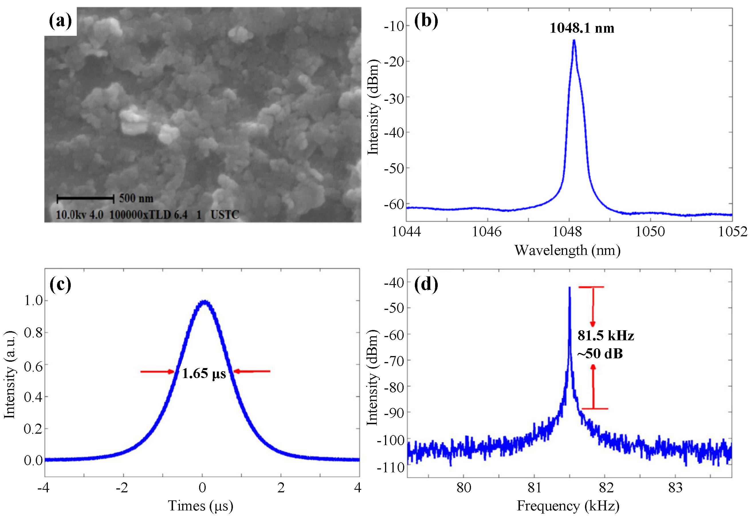
- Luo, Z.; Li, Y.; Zhong, M.; Huang, Y.; Wan, X.; Peng, J.; Weng, J. Nonlinear optical absorption of few-layer molybdenum diselenide (MoSe2) for passively mode-locked soliton fiber laser [Invited]. Photonics Res. 2015, 3, A79–A86. [Google Scholar] [CrossRef]
- Koo, J.; Park, J.; Lee, J.; Jhon, Y.M.; Lee, J.H. Femtosecond harmonic mode-locking of a fiber laser at 3.27 GHz using a bulk-like, MoSe2-based saturable absorber. Opt. Express 2016, 24, 10575–10589. [Google Scholar] [CrossRef]
- Liu, W.; Pang, L.; Han, H.; Liu, M.; Lei, M.; Fang, S.; Teng, H.; Wei, Z. Tungsten disulfide saturable absorbers for 67 fs mode-locked erbium-doped fiber lasers. Opt. Express 2017, 25, 2950–2959. [Google Scholar] [CrossRef] [PubMed] [Green Version]
- Liu, W.; Liu, M.; OuYang, Y.; Hou, H.; Lei, M.; Wei, Z. CVD-grown MoSe2 with high modulation depth for ultrafast mode-locked erbium-doped fiber laser. Nanotechnology 2018, 29, 394002. [Google Scholar] [CrossRef] [PubMed]
- Wang, S.; Yu, H.; Zhang, H.; Wang, A.; Zhao, M.; Chen, Y.; Mei, L.; Wang, J. Broadband few-layer MoS2 saturable absorbers. Adv. Mater. 2014, 26, 3538–3544. [Google Scholar] [CrossRef]
- Luo, Z.; Huang, Y.; Zhong, M.; Li, Y.; Wu, J.; Xu, B.; Xu, H.; Cai, Z.; Peng, J.; Weng, J. 1-, 1.5-, and 2-µm fiber lasers Q-switched by a broadband few-layer MoS2 saturable absorber. J. Light. Technol. 2014, 32, 4679–4686. [Google Scholar] [CrossRef]
- Kong, L.; Xie, G.; Yuan, P.; Qian, L.; Wang, S.; Yu, H.; Zhang, H. Passive Q-switching and Q-switched mode-locking operations of 2 µm Tm: CLNGG laser with MoS2 saturable absorber mirror. Photonics Res. 2015, 3, A47–A50. [Google Scholar] [CrossRef] [Green Version]
- Tian, Z.; Wu, K.; Kong, L.; Yang, N.; Wang, Y.; Chen, R.; Hu, W.; Xu, J.; Tang, Y. Mode-locked thulium fiber laser with MoS2. Laser Phys. Lett. 2015, 12, 065104. [Google Scholar] [CrossRef]
- Jung, M.; Lee, J.; Park, J.; Koo, J.; Jhon, Y.M.; Lee, J.H. Mode-locked, 1.94-µm, all-fiberized laser using WS2 based evanescent field interaction. Opt. Express 2015, 23, 19996–20006. [Google Scholar] [CrossRef]
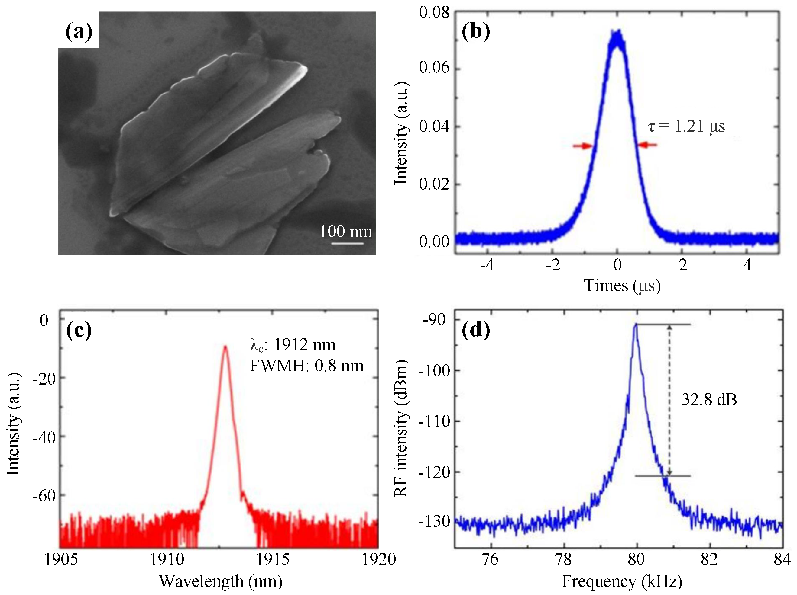
- Lee, J.; Koo, J.; Lee, J.; Jhon, Y.M.; Lee, J.H. All-fiberized, femtosecond laser at 1912 nm using a bulk-like MoSe2 saturable absorber. Opt. Mater. Express 2017, 7, 2968–2979. [Google Scholar] [CrossRef]
- Wang, J.; Xu, Z.; Liu, W.; Yan, P.; Lu, W.; Li, J.; Chen, H.; Jiang, Z.; Wang, J.; Zhang, W.; et al. Ultrafast thulium-doped fiber laser mode locked by monolayer WSe2. IEEE J. Sel. Top. Quantum Electron. 2018, 24, 1–6. [Google Scholar] [CrossRef]
- Fan, M.; Li, T.; Zhao, S.; Li, G.; Ma, H.; Gao, X.; Krankel, C.; Huber, G. Watt-level passively Q-switched Er:Lu2O3 laser at 2.84 µm using MoS2. Opt. Lett. 2016, 41, 540–543. [Google Scholar] [CrossRef]
- Wei, C.; Luo, H.; Zhang, H.; Li, C.; Xie, J.; Li, J.; Liu, Y. Passively Q-switched mid-infrared fluoride fiber laser around 3 µm using a tungsten disulfide (WS2) saturable absorber. Laser Phys. Lett. 2016, 13, 105108. [Google Scholar] [CrossRef]
- Liu, X.; Zhang, S.; Yan, Z.; Guo, L.; Fan, X.; Lou, F.; Wang, M.; Gao, P.; Guo, G.; Li, T.; et al. WSe2 as a saturable absorber for a passively Q-switched Ho,Pr:LLF laser at 295 μm. Opt. Mater. Express 2018, 8, 1213. [Google Scholar] [CrossRef]
- Zhang, S.; Liu, X.; Guo, L.; Fan, M.; Lou, F.; Gao, P.; Guo, G.; Yang, J.; Liu, J.; Li, T.; et al. Passively Q-switched Ho,Pr:LLF bulk slab laser at 2.95μm based on MoS2 saturable absorber. IEEE Photonics Technol. Lett. 2017, 29, 2258–2261. [Google Scholar] [CrossRef]
- Guo, C.; Wei, J.; Yan, P.; Luo, R.; Ruan, S.; Wang, J.; Guo, B.; Hua, P.; Lue, Q. Mode-locked fiber laser at 2.8 µm using a chemical-vapor-deposited WSe2 saturable absorber mirror. Appl. Phys. Express 2020, 13, 012013. [Google Scholar] [CrossRef]
- Chen, B.; Zhang, X.; Wu, K.; Wang, H.; Wang, J.; Chen, J. Q-switched fiber laser based on transition metal dichalcogenides MoS2, MoSe2, WS2, and WSe2. Opt. Express 2015, 23, 26723–26737. [Google Scholar] [CrossRef] [PubMed]
- Du, J.; Wang, Q.; Jiang, G.; Xu, C.; Zhao, C.; Xiang, Y.; Chen, Y.; Wen, S.; Zhang, H. Ytterbium-doped fiber laser passively mode locked by few-layer Molybdenum Disulfide (MoS2) saturable absorber functioned with evanescent field interaction. Sci. Rep. 2014, 4, 6346. [Google Scholar] [CrossRef]
- Liu, S.; Lv, R.; Wang, Y.; Wang, J.; Wang, Y.; Wang, H. Passively mode-locked fiber laser with WS2/SiO2 saturable absorber fabricated by Sol-Gel technique. ACS Appl. Mater. Interfaces 2020, 12, 29625–29630. [Google Scholar] [CrossRef] [PubMed]
- Cheng, C.; Li, Z.; Dong, N.; Wang, J.; Chen, F. Tin diselenide as a new saturable absorber for generation of laser pulses at 1 μm. Opt. Express 2017, 25, 6132–6140. [Google Scholar] [CrossRef]
- Li, J.; Zhao, Y.; Chen, Q.; Niu, K.; Sun, R.; Zhang, H. Passively mode-locked ytterbium-doped fiber laser based on SnS2 as saturable absorber. IEEE Photonics J. 2017, 9, 1–7. [Google Scholar] [CrossRef]
- Niu, K.; Chen, Q.; Sun, R.; Man, B.; Zhang, H. Passively Q-switched erbium-doped fiber laser based on SnS2 saturable absorber. Opt. Mater. Express 2017, 7, 3934–3943. [Google Scholar] [CrossRef]
- Niu, K.; Sun, R.; Chen, Q.; Man, B.; Zhang, H. Passively mode-locked Er-doped fiber laser based on SnS2 nanosheets as a saturable absorber. Photonics Res. 2018, 6, 72–76. [Google Scholar] [CrossRef]
- Yao, Y.; Zhang, F.; Chen, B.; Zhao, Y.; Cui, N.; Sun, D.; Liu, S.; Zhang, Y.; Zhang, H.; Zhang, H. Nonlinear optical property and mid-infrared Q-switched laser application at 2.8 µm of PtSe2 material. Opt. Laser Technol. 2021, 139, 106983. [Google Scholar] [CrossRef]
- Chen, Y.; Chen, S.; Liu, J.; Gao, Y.; Zhang, W. Sub-300 femtosecond soliton tunable fiber laser with all-anomalous dispersion passively mode locked by black phosphorus. Opt. Express 2016, 24, 13316–13324. [Google Scholar] [CrossRef]
- Song, Y.; Chen, S.; Zhang, Q.; Li, L.; Zhao, L.; Zhang, H.; Tang, D. Vector soliton fiber laser passively mode locked by few layer black phosphorus-based optical saturable absorber. Opt. Express 2016, 24, 25933–25942. [Google Scholar] [CrossRef]
- Yun, L. Black phosphorus saturable absorber for dual-wavelength polarization-locked vector soliton generation. Opt. Express 2017, 25, 32380–32385. [Google Scholar] [CrossRef]
- Jin, X.; Hu, G.; Zhang, M.; Hu, Y.; Albrow-Owen, T.; Howe, R.C.T.; Wu, T.C.; Wu, Q.; Zheng, Z.; Hasan, T. 102 fs pulse generation from a long-term stable, inkjet-printed black phosphorus-mode-locked fiber laser. Opt. Express 2018, 26, 12506–12513. [Google Scholar] [CrossRef]
- Zhang, B.; Lou, F.; Zhao, R.; He, J.; Li, J.; Su, X.; Ning, J.; Yang, K. Exfoliated layers of black phosphorus as saturable absorber for ultrafast solid-state laser. Opt. Lett. 2015, 40, 3691–3694. [Google Scholar] [CrossRef]
- Ma, J.; Lu, S.; Guo, Z.; Xu, X.; Zhang, H.; Tang, D.; Fan, D. Few-layer black phosphorus based saturable absorber mirror for pulsed solid-state lasers. Opt. Express 2015, 23, 22643–22648. [Google Scholar] [CrossRef]
- Al-Masoodi, A.H.H.; Ahmed, M.H.M.; Latiff, A.A.; Arof, H.; Harun, S.W. Q-switched ytterbium-doped fiber laser using black phosphorus as saturable absorber. Chin. Phys. Lett. 2016, 33, 054206. [Google Scholar] [CrossRef] [Green Version]
- Su, X.; Wang, Y.; Zhang, B.; Zhao, R.; Yang, K.; He, J.; Hu, Q.; Jia, Z.; Tao, X. Femtosecond solid-state laser based on a few-layered black phosphorus saturable absorber. Opt. Lett. 2016, 41, 1945–1948. [Google Scholar] [CrossRef]
- Rashid, F.A.A.; Azzuhri, S.R.; Salim, M.A.M.; Shaharuddin, R.A.; Ismail, M.A.; Ismail, M.F.; Razak, M.Z.A.; Ahmad, H. Using a black phosphorus saturable absorber to generate dual wavelengths in a Q-switched ytterbium-doped fiber laser. Laser Phys. Lett. 2016, 13, 085102. [Google Scholar] [CrossRef] [Green Version]
- Ahmad, H.; Salim, M.A.M.; Thambiratnam, K.; Norizan, S.F.; Harun, S.W. A black phosphorus-based tunable Q-switched ytterbium fiber laser. Laser Phys. Lett. 2016, 13, 095103. [Google Scholar] [CrossRef]
- Huang, K.X.; Lu, B.L.; Li, D.; Qi, X.Y.; Chen, H.W.; Wang, N.; Wen, Z.R.; Bai, J.T. Black phosphorus flakes covered microfiber for Q-switched ytterbium-doped fiber laser. Appl. Opt. 2017, 56, 6427–6431. [Google Scholar] [CrossRef]
- Wang, D.; Song, H.; Long, X.; Li, L. Switchable and tunable multi-wavelength emissions in pulsed ytterbium fiber lasers with black phosphorus saturable absorbers and polarization-maintaining fiber Bragg gratings. Opt. Commun. 2019, 452, 373–379. [Google Scholar] [CrossRef]
- Yu, H.; Zheng, X.; Yin, K.; Cheng, X.; Jiang, T. Nanosecond passively Q-switched thulium/holmium-doped fiber laser based on black phosphorus nanoplatelets. Opt. Mater. Express 2016, 6, 603–609. [Google Scholar] [CrossRef]
- Chu, Z.Z.; Liu, J.; Guo, Z.N.; Zhang, H. 2 µm passively Q-switched laser based on black phosphorus. Opt. Mater. Express 2016, 6, 2374–2379. [Google Scholar] [CrossRef]
- Zhang, H.; He, J.; Wang, Z.; Hou, J.; Zhang, B.; Zhao, R.; Han, K.; Yang, K.; Nie, H.; Sun, X. Dual-wavelength, passively Q-switched Tm:YAP laser with black phosphorus saturable absorber. Opt. Mater. Express 2016, 6, 2328–2335. [Google Scholar] [CrossRef]
- Pawliszewska, M.; Ge, Y.; Li, Z.; Zhang, H.; Sotor, J. Fundamental and harmonic mode-locking at 2.1 µm with black phosphorus saturable absorber. Opt. Express 2017, 25, 16916–16921. [Google Scholar] [CrossRef]
- Qin, Z.; Xie, G.; Zhao, C.; Wen, S.; Yuan, P.; Qian, L. Mid-infrared mode-locked pulse generation with multilayer black phosphorus as saturable absorber. Opt. Lett. 2016, 41, 56–59. [Google Scholar] [CrossRef]
- Kong, L.; Qin, Z.; Xie, G.; Guo, Z.; Zhang, H.; Yuan, P.; Qian, L. Black phosphorus as broadband saturable absorber for pulsed lasers from 1 µm to 2.7 µm wavelength. Laser Phys. Lett. 2016, 13, 045801. [Google Scholar] [CrossRef] [Green Version]
- Liu, J.; Liu, J.; Guo, Z.; Zhang, H.; Ma, W.; Wang, J.; Su, L. Dual-wavelength Q-switched Er:SrF2 laser with a black phosphorus absorber in the mid-infrared region. Opt. Express 2016, 24, 30289–30295. [Google Scholar] [CrossRef]
- Woodward, R.I.; Majewski, M.R.; Macadam, N.; Hu, G.; Albrow-Owen, T.; Hasan, T.; Jackson, S.D. Q-switched Dy:ZBLAN fiber lasers beyond 3 µm: Comparison of pulse generation using acousto-optic modulation and inkjet-printed black phosphorus. Opt. Express 2019, 27, 15032–15045. [Google Scholar] [CrossRef]
- Guo, Z.; Zhang, H.; Lu, S.; Wang, Z.; Tang, S.; Shao, J.; Sun, Z.; Xie, H.; Wang, H.; Yu, X.F.; et al. From black phosphorus to phosphorene: Basic solvent exfoliation, evolution of raman scattering, and applications to ultrafast photonics. Adv. Funct. Mater. 2015, 25, 6996–7002. [Google Scholar] [CrossRef]
- Morita, A. Semiconducting black phosphorus. Appl. Phys. A 1986, 39, 227–242. [Google Scholar] [CrossRef]
- Tran, V.; Soklaski, R.; Liang, Y.; Yang, L. Layer-controlled band gap and anisotropic excitons in few-layer black phosphorus. Phys. Rev. B 2014, 89, 235319. [Google Scholar] [CrossRef] [Green Version]
- Island, J.O.; Steele, G.A.; van der Zant, H.S.; Castellanos-Gomez, A. Environmental instability of few-layer black phosphorus. 2D Mater. 2015, 2, 011002. [Google Scholar] [CrossRef] [Green Version]
- Wang, X.; Jones, A.M.; Seyler, K.L.; Tran, V.; Jia, Y.; Zhao, H.; Wang, H.; Yang, L.; Xu, X.; Xia, F. Highly anisotropic and robust excitons in monolayer black phosphorus. Nat. Nanotechnol. 2015, 10, 517–521. [Google Scholar] [CrossRef] [Green Version]
- Castellanos-Gomez, A.; Vicarelli, L.; Prada, E.; Island, J.O.; Narasimha-Acharya, K.; Blanter, S.I.; Groenendijk, D.J.; Buscema, M.; Steele, G.A.; Alvarez, J. Isolation and characterization of few-layer black phosphorus. 2D Mater. 2014, 1, 025001. [Google Scholar] [CrossRef]
- Mikulla, B.; Leng, L.; Sears, S.; Collings, B.C.; Arend, M.; Bergman, K. Broad-band high-repetition-rate source for spectrally sliced WDM. IEEE Photonics Technol. Lett. 1999, 11, 418–420. [Google Scholar] [CrossRef]
- McFerran, J.J. Échelle spectrograph calibration with a frequency comb based on a harmonically mode-locked fiber laser: A proposal. Appl. Opt. 2009, 48, 2752–2759. [Google Scholar] [CrossRef]
- Jhon, Y.I.; Koo, J.; Anasori, B.; Seo, M.; Lee, J.H.; Gogotsi, Y.; Jhon, Y.M. Metallic MXene saturable absorber for femtosecond mode-locked lasers. Adv. Mater. 2017, 29, 1702496. [Google Scholar] [CrossRef]
- Jiang, X.; Liu, S.; Liang, W.; Luo, S.; He, Z.; Ge, Y.; Wang, H.; Cao, R.; Zhang, F.; Wen, Q.; et al. Broadband nonlinear photonics in few-layer MXene Ti3C2Tx (T = F, O, or OH). Laser Photonics Rev. 2018, 12, 1700229. [Google Scholar] [CrossRef]
- Kim, J.J.; Kim, H.; Koo, C.M.; Lee, J.H.; Lee, S.B.; Lee, K. Femtosecond mode-locked fiber laser Using an etched optical fiber immersed in liquid Mxene as a saturable absorber. In Proceedings of the 23rd Opto-Electronics and Communications Conference, Institute of Electrical and Electronics Engineers Inc., Jeju, Korea, 2–6 July 2018; p. 8730133. [Google Scholar] [CrossRef]
- Li, J.; Zhang, Z.; Du, L.; Miao, L.; Yi, J.; Huang, B.; Zou, Y.; Zhao, C.; Wen, S. Highly stable femtosecond pulse generation from a MXene Ti3C2Tx (T = F, O, or OH) mode-locked fiber laser. Photonics Res. 2019, 7, 260–264. [Google Scholar] [CrossRef]
- Feng, J.; Li, X.; Feng, T.; Wang, Y.; Liu, J.; Zhang, H. Harmonic mode-locked Er-doped fiber laser by evanescent field-based MXene Ti3C2Tx (T = F, O, or OH) saturable absorber. Ann. Phys. 2020, 532, 1900437. [Google Scholar] [CrossRef]
- Wu, Q.; Jin, X.; Chen, S.; Jiang, X.; Hu, Y.; Jiang, Q.; Wu, L.; Li, J.; Zheng, Z.; Zhang, M.; et al. MXene-based saturable absorber for femtosecond mode-locked fiber lasers. Opt. Express 2019, 27, 10159–10170. [Google Scholar] [CrossRef] [PubMed]
- Huang, W.; Ma, C.; Li, C.; Zhang, Y.; Hu, L.; Chen, T.; Tang, Y.; Ju, J.; Zhang, H. Highly stable MXene (V2CTx)-based harmonic pulse generation. Nanophotonics 2020, 9, 2577–2585. [Google Scholar] [CrossRef]
- Li, G.; Yang, L.; Zhao, R.; Wang, F.; Nie, H.; Wang, R.; Yang, K.; Zhang, B.; He, J. Generation of a square-shaped pulse in mode-locked fiber lasers with a microfiber-based few-layer Nb2C saturable absorber. Appl. Opt. 2020, 59, 11240–11245. [Google Scholar] [CrossRef] [PubMed]
- Jafry, A.A.A.; Muhammad, A.R.; Kasim, N.; Rosol, A.H.A.; Rusdi, M.F.M.; Ab Alim, N.N.N.; Harun, S.W.; Yupapin, P. Ultrashort pulse generation with MXene Ti3C2Tx embedded in PVA and deposited onto D-shaped fiber. Opt. Laser Technol. 2021, 136, 106780. [Google Scholar] [CrossRef]
- Feng, X.Y.; Ding, B.Y.; Liang, W.Y.; Zhang, F.; Ning, T.Y.; Liu, J.; Zhang, H. MXene Ti3C2Tx absorber for a 1.06 μm passively Q-switched ceramic laser. Laser Phys. Lett. 2018, 15, 085805. [Google Scholar] [CrossRef]
- Sun, X.; Zhang, B.; Yan, B.; Li, G.; Nie, H.; Yang, K.; Zhang, C.; He, J. Few-layer Ti3C2Tx (T = O, OH, or F) saturable absorber for a femtosecond bulk laser. Opt. Lett. 2018, 43, 3862–3865. [Google Scholar] [CrossRef]
- Shi, Y.; Xu, N.; Wen, Q. Ti2CTx (T = O, OH or F) nanosheets as new broadband saturable absorber for ultrafast photonics. J. Light. Technol. 2020, 38, 1975–1980. [Google Scholar] [CrossRef]
- Ma, C.; Huang, W.; Wang, Y.; Adams, J.; Wang, Z.; Liu, J.; Song, Y.; Ge, Y.; Guo, Z.; Hu, L.; et al. MXene saturable absorber enabled hybrid mode-locking technology: A new routine of advancing femtosecond fiber lasers performance. Nanophotonics 2020, 9, 2451–2458. [Google Scholar] [CrossRef]
- Zu, Y.; Zhang, C.; Guo, X.; Liang, W.; Liu, J.; Su, L.; Zhang, H. A solid-state passively Q-switched Tm,Gd:CaF2laser with a Ti3C2TxMXene absorber near 2 µm. Laser Phys. Lett. 2019, 16, 015803. [Google Scholar] [CrossRef]
- Jiang, Q.; Zhang, M.; Zhang, Q.; Jin, X.; Wu, Q.; Jiang, X.; Zhang, H.; Zheng, Z. Thulium-doped mode-locked fiber laser with MXene saturable absorber. In Proceedings of the CLEO: Science and Innovations, Optical Society of America, San Jose, CA, USA, 5–10 May 2019; p. SF3O.3. [Google Scholar] [CrossRef]
- Wang, S.; Li, L.; Song, Y.F.; Tang, D.Y.; Shen, D.Y.; Zhao, L.M. Vector soliton and noise-like pulse generation using a Ti3C2 MXene material in a fiber laser. Front. Inf. Technol. Electron. Eng. 2020, 22, 318–324. [Google Scholar] [CrossRef]
- Ahmad, H.; Ramli, R.; Yusoff, N.; Samion, M.Z.; Ismail, M.F.; Bayang, L.; Aidit, S.N.; Zamzuri, A.K.; Thambiratnam, K. 155 nm-wideband and tunable q-switched fiber laser using an MXene Ti3C2Tx coated microfiber based saturable absorber. Laser Phys. Lett. 2020, 17, 085103. [Google Scholar] [CrossRef]
- Gao, L.; Ma, C.; Wei, S.; Kuklin, A.V.; Zhang, H.; Agren, H. Applications of Few-Layer Nb2C MXene: Narrow-Band Photodetectors and Femtosecond Mode-Locked Fiber Lasers. ACS Nano 2021, 15, 954–965. [Google Scholar] [CrossRef]
- Niu, Z.; Feng, T.; Yang, K.; Li, T.; Zhao, J.; Li, G.; Li, D.; Zhao, S.; Jiang, X.; Zhang, H.; et al. MXene Ti3C2Tx (T = F, O, or OH) saturable absorber for a 2 µm doubly Q-switched laser with AOM. Opt. Laser Technol. 2021, 134, 106642. [Google Scholar] [CrossRef]
- Zhou, L.; Wei, C.; Wang, D.; Chi, H.; Li, Q.; Zhang, H.; Liu, Y. Q-switched mid-infrared Er3+: ZBLAN fiber laser at 2.8 µm with a MXene-based Saturable Absorber. In Proceedings of the 2019 Asia Communications and Photonics Conference, Optical Society of America, No. 1736 Tianfu Avenue North, OSA Technical Digest, Chengdu, China, 2–5 November 2019; p. S4A.2. [Google Scholar]
- Gayathri, B.; Xiantao, J.; Han, Z.; Feng, C.; Ziqi, L.; Stuart, D.J.; Alex, F. Mode-locked mid-IR fibre laser based on 2D nanomaterials. In AOS Australian Conference on Optical Fibre Technology (ACOFT) and Australian Conference on Optics, Lasers, and Spectroscopy (ACOLS) 2019; International Society for Optics and Photonics: Bellingham, WA, USA, 2019; Volume 11200. [Google Scholar] [CrossRef]
- Wei, C.; Zhou, L.; Wang, D.; Chi, H.; Huang, H.; Zhang, H.; Liu, Y. MXene-Ti3C2Tx for watt-level high-efficiency pulse generation in a 2.8 µm mid-infrared fiber laser. Photonics Res. 2020, 8, 972–977. [Google Scholar] [CrossRef]
- Feng, C.; Qiao, W.; Liu, Y.; Huang, J.; Liang, Y.; Zhao, Y.; Song, Y.; Li, T. Modulation of MXene Nb2CTx saturable absorber for passively Q-switched 2.85 microm Er:Lu2O3 laser. Opt. Lett. 2021, 46, 1385–1388. [Google Scholar] [CrossRef] [PubMed]
- Dong, Y.; Chertopalov, S.; Maleski, K.; Anasori, B.; Hu, L.; Bhattacharya, S.; Rao, A.M.; Gogotsi, Y.; Mochalin, V.N.; Podila, R. Saturable absorption in 2D Ti3C2 MXene thin films for passive photonic diodes. Adv. Mater. 2018, 30, 1705714. [Google Scholar] [CrossRef] [PubMed]
- Geim, A.K.; Grigorieva, I.V. Van der Waals heterostructures. Nature 2013, 499, 419–425. [Google Scholar] [CrossRef] [PubMed]
- Mu, H.; Wang, Z.; Yuan, J.; Xiao, S.; Chen, C.; Chen, Y.; Chen, Y.; Song, J.; Wang, Y.; Xue, Y.; et al. Graphene-Bi2Te3 heterostructure as saturable absorber for short pulse generation. ACS Photonics 2015, 2, 832–841. [Google Scholar] [CrossRef]
- Jiang, Y.; Miao, L.; Jiang, G.; Chen, Y.; Qi, X.; Jiang, X.f.; Zhang, H.; Wen, S. Broadband and enhanced nonlinear optical response of MoS2/graphene nanocomposites for ultrafast photonics applications. Sci. Rep. 2015, 5, 1–12. [Google Scholar] [CrossRef] [Green Version]
- Liu, S.; Li, Z.; Ge, Y.; Wang, H.; Yue, R.; Jiang, X.; Li, J.; Wen, Q.; Zhang, H. Graphene/phosphorene nano-heterojunction: Facile synthesis, nonlinear optics, and ultrafast photonics applications with enhanced performance. Photonics Res. 2017, 5, 662–668. [Google Scholar] [CrossRef]
- Li, Z.; Cheng, C.; Dong, N.; Romero, C.; Lu, Q.; Wang, J.; de Aldana, J.R.V.; Tan, Y.; Chen, F. Q-switching of waveguide lasers based on graphene/WS2 van der Waals heterostructure. Photonics Res. 2017, 5, 406–410. [Google Scholar] [CrossRef]
- Tan, Y.; Liu, X.; He, Z.; Liu, Y.; Zhao, M.; Zhang, H.; Chen, F. Tuning of interlayer coupling in large-area graphene/WSe2 van der Waals heterostructure via ion irradiation: Optical evidences and photonic applications. ACS Photonics 2017, 4, 1531–1538. [Google Scholar] [CrossRef] [Green Version]
- You, Z.Y.; Sun, Y.J.; Sun, D.L.; Zhu, Z.J.; Wang, Y.; Li, J.F.; Tu, C.Y.; Xu, J.L. High performance of a passively Q-switched mid-infrared laser with Bi2Te3/graphene composite SA. Opt. Lett. 2017, 42, 871–874. [Google Scholar] [CrossRef]
- Zhao, G.; Lv, X.; Xie, Z.; Xu, J. 2.8 µm Passively Q-switched solid state pulse laser based on MoS2/Graphene heterojunction. In Proceedings of the 2017 Conference on Lasers and Electro-Optics Pacific Rim (CLEO-PR), Singapore, 31 July–4 August 2017; p. s1175. [Google Scholar] [CrossRef]
- Liu, W.; Zhu, Y.N.; Liu, M.; Wen, B.; Fang, S.; Teng, H.; Lei, M.; Liu, L.M.; Wei, Z. Optical properties and applications for MoS2-Sb2Te3-MoS2 heterostructure materials. Photonics Res. 2018, 6, 220–227. [Google Scholar] [CrossRef]
- Xue, Y.; Xie, Z.; Ye, Z.; Hu, X.; Xu, J.; Zhang, H. Enhanced saturable absorption of MoS2 black phosphorus composite in 2 µm passively Q-switched Tm:YAP laser. Chin. Opt. Lett. 2018, 16, 020018. [Google Scholar] [CrossRef] [Green Version]
- Liu, W.; Liu, M.; Liu, B.; Quhe, R.; Lei, M.; Fang, S.; Teng, H.; Wei, Z. Nonlinear optical properties of MoS2-WS2 heterostructure in fiber lasers. Opt. Express 2019, 27, 6689–6699. [Google Scholar] [CrossRef] [PubMed]
- Xia, X.; Ma, C.; Chen, H.; Khan, K.; Tateen, A.K.; Xiao, Q. Nonlinear optical properties and ultrafast photonics of 2D BP/Ti3C2 heterostructures. Opt. Mater. 2021, 112, 110809. [Google Scholar] [CrossRef]
- Du, W.; Li, H.; Lan, C.; Li, C.; Li, J.; Wang, Z.; Liu, Y. Graphene/WS2 heterostructure saturable absorbers for ultrashort pulse generation in L-band passively mode-locked fiber lasers. Opt. Express 2020, 28, 11514–11523. [Google Scholar] [CrossRef]
- Wang, Z.; Zhang, B.; Liu, J.; Song, Y.; Zhang, H. Recent developments in mid-infrared fiber lasers: Status and challenges. Opt. Laser Technol. 2020, 132, 106497. [Google Scholar] [CrossRef]
- Zhang, W.; Wang, Q.; Chen, Y.; Wang, Z.; Wee, A.T. Van der Waals stacked 2D layered materials for optoelectronics. 2D Mater. 2016, 3, 022001. [Google Scholar] [CrossRef]
- Jiang, T.; Yin, K.; Wang, C.; You, J.; Ouyang, H.; Miao, R.; Zhang, C.; Wei, K.; Li, H.; Chen, H.; et al. Ultrafast fiber lasers mode-locked by two-dimensional materials: Review and prospect. Photonics Res. 2020, 8, 78–90. [Google Scholar] [CrossRef]
- Ye, L.; Li, H.; Chen, Z.; Xu, J. Near-infrared photodetector based on MoS2/black phosphorus heterojunction. ACS Photonics 2016, 3, 692–699. [Google Scholar] [CrossRef]
- Qiao, H.; Yuan, J.; Xu, Z.; Chen, C.; Lin, S.; Wang, Y.; Song, J.; Liu, Y.; Khan, Q.; Hoh, H.Y.; et al. Broadband photodetectors based on graphene-Bi2Te3 heterostructure. ACS Nano 2015, 9, 1886–1894. [Google Scholar] [CrossRef]
- Chen, C.; Xie, X.; Anasori, B.; Sarycheva, A.; Makaryan, T.; Zhao, M.; Urbankowski, P.; Miao, L.; Jiang, J.; Gogotsi, Y. MoS2-on-MXene heterostructures as highly reversible anode materials for lithium-ion batteries. Angew. Chem. Int. Ed. 2018, 57, 1846–1850. [Google Scholar] [CrossRef]
- Du, Y.T.; Kan, X.; Yang, F.; Gan, L.Y.; Schwingenschlögl, U. MXene/graphene heterostructures as high-performance electrodes for Li-ion batteries. ACS Appl. Mater. Interfaces 2018, 10, 32867–32873. [Google Scholar] [CrossRef]
- Georgiou, T.; Jalil, R.; Belle, B.D.; Britnell, L.; Gorbachev, R.V.; Morozov, S.V.; Kim, Y.J.; Gholinia, A.; Haigh, S.J.; Makarovsky, O.; et al. Vertical field-effect transistor based on graphene-WS2 heterostructures for flexible and transparent electronics. Nat. Nanotechnol. 2013, 8, 100–103. [Google Scholar] [CrossRef]
- Yan, P.; Liu, A.; Chen, Y.; Chen, H.; Ruan, S.; Guo, C.; Chen, S.; Li, I.L.; Yang, H.; Hu, J.; et al. Microfiber-based WS2-film saturable absorber for ultra-fast photonics. Opt. Mater. Express 2015, 5, 479–489. [Google Scholar] [CrossRef]
- Wei, C.; Zhu, X.; Wang, F.; Xu, Y.; Balakrishnan, K.; Song, F.; Norwood, R.A.; Peyghambarian, N. Graphene Q-switched 2.78 µm Er3+-doped fluoride fiber laser. Opt. Lett. 2013, 38, 3233–3236. [Google Scholar] [CrossRef] [PubMed]
- Wang, S.; Tang, Y.; Yang, J.; Zhong, H.; Fan, D. MoS2 Q-switched 2.8 µm Er:ZBLAN fiber laser. Laser Phys. 2019, 29, 025101. [Google Scholar] [CrossRef]
- Li, Y.; He, Y.; Cai, Y.; Chen, S.; Liu, J.; Chen, Y.; Yuanjiang, X. Black phosphorus: Broadband nonlinear optical absorption and application. Laser Phys. Lett. 2018, 15, 025301. [Google Scholar] [CrossRef]
- Cihan, C.; Kocabas, C.; Demirbas, U.; Sennaroglu, A. Graphene mode-locked femtosecond Alexandrite laser. Opt. Lett. 2018, 43, 3969–3972. [Google Scholar] [CrossRef]
- Komsa, H.P.; Krasheninnikov, A.V. Electronic structures and optical properties of realistic transition metal dichalcogenide heterostructures from first principles. Phys. Rev. B 2013, 88, 085318. [Google Scholar] [CrossRef] [Green Version]
- Zhao, W.; Ribeiro, R.M.; Toh, M.; Carvalho, A.; Kloc, C.; Castro Neto, A.; Eda, G. Origin of indirect optical transitions in few-layer MoS2, WS2, and WSe2. Nano Lett. 2013, 13, 5627–5634. [Google Scholar] [CrossRef] [Green Version]
- Qin, Z.; Hai, T.; Xie, G.; Ma, J.; Yuan, P.; Qian, L.; Li, L.; Zhao, L.; Shen, D. Black phosphorus Q-switched and mode-locked mid-infrared Er:ZBLAN fiber laser at 3.5 µm wavelength. Opt. Express 2018, 26, 8224–8231. [Google Scholar] [CrossRef]
- Purdie, D.G.; Popa, D.; Wittwer, V.J.; Jiang, Z.; Bonacchini, G.; Torrisi, F.; Milana, S.; Lidorikis, E.; Ferrari, A.C. Few-cycle pulses from a graphene mode-locked all-fiber laser. Appl. Phys. Lett. 2015, 106, 253101. [Google Scholar] [CrossRef] [Green Version]
- Yu, C.; Chujun, Z.; Shuqing, C.; Juan, D.; Pinghua, T.; Guobao, J.; Han, Z.; Shuangchun, W.; Dingyuan, T. Large energy, wavelength widely tunable, topological insulator Q-switched erbium-doped fiber laser. IEEE J. Sel. Top. Quantum Electron. 2014, 20, 315–322. [Google Scholar] [CrossRef]
- Lee, J.; Kim, Y.; Lee, K.; Lee, J.H. Femtosecond mode-locking of a fiber laser using a CoSb3-skutterudite-based saturable absorber. Photonics Res. 2018, 6, C36–C43. [Google Scholar] [CrossRef] [Green Version]
- Liu, W.J.; Liu, M.L.; OuYang, Y.Y.; Hou, H.R.; Ma, G.L.; Lei, M.; Wei, Z.Y. Tungsten diselenide for mode-locked erbium-doped fiber lasers with short pulse duration. Nanotechnology 2018, 29, 174002. [Google Scholar] [CrossRef]
- Wei, C.; Chi, H.; Jiang, S.; Zheng, L.; Zhang, H.; Liu, Y. Long-term stable platinum diselenide for nanosecond pulse generation in a 3-μm mid-infrared fiber laser. Opt. Express 2020, 28, 33758–33766. [Google Scholar] [CrossRef]
- Yan, X.; Jiang, M.; Li, E.; Kang, X.; Ren, Z.; Li, D.; Wang, T.; Lu, B. Tunable high-order harmonic and dual-wavelength mode-locking in Er-doped fiber laser based on Ti3C2Tx-MXene. Appl. Phys. Express 2021, 14, 012009. [Google Scholar] [CrossRef]
- Zhang, C.; Zhang, F.; Fan, X.; Yang, J.; Liu, J.; Zhang, H. Passively Q-switched operation of in-band pumped Ho:YLF based on Ti3C2Tx MXene. Infrared Phys. Technol. 2019, 103, 103076. [Google Scholar] [CrossRef]
- Li, G.; Liu, J.; Wang, F.; Nie, H.; Wang, R.; Yang, K.; Zhang, B.; He, J. Third-order nonlinear optical response of few-layer MXene Nb2C and applications for square-wave laser pulse generation. Adv. Mater. Interfaces 2021, 8, 2001805. [Google Scholar] [CrossRef]
- Tuo, M.; Xu, C.; Mu, H.; Bao, X.; Wang, Y.; Xiao, S.; Ma, W.; Li, L.; Tang, D.; Zhang, H.; et al. Ultrathin 2D transition metal carbides for ultrafast pulsed fiber lasers. ACS Photonics 2018, 5, 1808–1816. [Google Scholar] [CrossRef]
- Sun, X.; Zhang, B.; Li, Y.; Luo, X.; Li, G.; Chen, Y.; Zhang, C.; He, J. Tunable ultrafast nonlinear optical properties of graphene/MoS2 van der Waals heterostructures and their application in solid-state bulk lasers. ACS Nano 2018, 12, 11376–11385. [Google Scholar] [CrossRef]
- Meng, S.; Kong, T.; Ma, W.; Wang, H.; Zhang, H. 2D Crystal–Based Fibers: Status and Challenges. Small 2019, 15, 1902691. [Google Scholar] [CrossRef] [PubMed]
- Zhang, H. Ultrathin two-dimensional nanomaterials. ACS Nano 2015, 9, 9451–9469. [Google Scholar] [CrossRef] [PubMed]
- Liu, Y.; Xiao, C.; Li, Z.; Xie, Y. Vacancy engineering for tuning electron and phonon structures of two-dimensional materials. Adv. Energy Mater. 2016, 6, 1600436. [Google Scholar] [CrossRef]
- Jung, N.; Kim, B.; Crowther, A.C.; Kim, N.; Nuckolls, C.; Brus, L. Optical reflectivity and raman scattering in few-layer-thick graphene highly doped by K and Rb. ACS Nano 2011, 5, 5708–5716. [Google Scholar] [CrossRef]
- Hartmann, S.J.; Iurchenkova, A.A.; Kallio, T.; Fedorovskaya, E.O. Electrochemical properties of nitrogen and oxygen doped reduced graphene oxide. Energies 2020, 13, 312. [Google Scholar] [CrossRef] [Green Version]
- Shao, L.S.; Li, J.J.; Guang, Y.; Zhang, Y.L.; Zhang, H.; Che, X.Y.; Wang, Y.H. PVA/polyethyleneimine-functionalized graphene composites with optimized properties. Mater. Des. 2016, 99, 235–242. [Google Scholar] [CrossRef]
- Sun, Z.; Hasan, T.; Torrisi, F.; Popa, D.; Privitera, G.; Wang, F.; Bonaccorso, F.; Basko, D.M.; Ferrari, A.C. Graphene mode-locked ultrafast laser. ACS Nano 2010, 4, 803–810. [Google Scholar] [CrossRef] [Green Version]
- Xia, H.; Li, H.; Lan, C.; Li, C.; Zhang, X.; Zhang, S.; Liu, Y. Ultrafast erbium-doped fiber laser mode-locked by a CVD-grown molybdenum disulfide (MoS2) saturable absorber. Opt. Express 2014, 22, 17341–17348. [Google Scholar] [CrossRef]
- Novoselov, K.S.; Mishchenko, A.; Carvalho, A.; Neto, A.H.C. 2D materials and van der Waals heterostructures. Science 2016, 353, aac9439. [Google Scholar] [CrossRef] [Green Version]
- Zhou, K.G.; Withers, F.; Cao, Y.; Hu, S.; Yu, G.L.; Casiraghi, C. Raman modes of MoS2 Used as fingerprint of van der waals interactions in 2-D crystal-based heterostructures. ACS Nano 2014, 8, 9914–9924. [Google Scholar] [CrossRef]
- Sakakura, M.; Lei, Y.H.; Wang, L.; Yu, Y.H.; Kazansky, P.G. Ultralow-loss geometric phase and polarization shaping by ultrafast laser writing in silica glass. Light. Sci. Appl. 2020, 9, 15. [Google Scholar] [CrossRef] [Green Version]
- Baig, Z.; Mamat, O.; Mustapha, M.; Mumtaz, A.; Munir, K.S.; Sarfraz, M. Investigation of tip sonication effects on structural quality of graphene nanoplatelets (GNPs) for superior solvent dispersion. Ultrason. Sonochem. 2018, 45, 133–149. [Google Scholar] [CrossRef]
- Lee, X.J.; Hiew, B.Y.Z.; Lai, K.C.; Lee, L.Y.; Gan, S.; Thangalazhy-Gopakumar, S.; Rigby, S. Review on graphene and its derivatives: Synthesis methods and potential industrial implementation. J. Taiwan Inst. Chem. Eng. 2019, 98, 163–180. [Google Scholar] [CrossRef]
- Xu, J.; Hu, J.; Li, Q.; Wang, R.; Li, W.; Guo, Y.; Zhu, Y.; Liu, F.; Ullah, Z.; Dong, G.; et al. Fast batch production of high-quality graphene films in a sealed thermal molecular movement system. Small 2017, 13, 1700651. [Google Scholar] [CrossRef] [PubMed]
- Goyal, V.; Teweldebrhan, D.; Balandin, A.A. Mechanically-exfoliated stacks of thin films of Bi2Te3 topological insulators with enhanced thermoelectric performance. Appl. Phys. Lett. 2010, 97, 133117. [Google Scholar] [CrossRef] [Green Version]
- Krumrain, J.; Mussler, G.; Borisova, S.; Stoica, T.; Plucinski, L.; Schneider, C.; Grützmacher, D. MBE growth optimization of topological insulator Bi2Te3 films. J. Cryst. Growth 2011, 324, 115–118. [Google Scholar] [CrossRef]
- Aabdin, Z.; Peranio, N.; Winkler, M.; Bessas, D.; König, J.; Hermann, R.; Böttner, H.; Eibl, O. Sb2Te3 and Bi2Te3 thin films grown by room-temperature MBE. J. Electron. Mater. 2012, 41, 1493–1497. [Google Scholar] [CrossRef]
- Fei, F.; Wei, Z.; Wang, Q.; Lu, P.; Wang, S.; Qin, Y.; Pan, D.; Zhao, B.; Wang, X.; Sun, J.; et al. Solvothermal synthesis of lateral heterojunction Sb2Te3/Bi2Te3 nanoplates. Nano Lett. 2015, 15, 5905–5911. [Google Scholar] [CrossRef]
- Tian, W.; Yu, W.; Shi, J.; Wang, Y. The property, preparation and application of topological insulators: A review. Materials 2017, 10, 814. [Google Scholar] [CrossRef] [Green Version]
- Brom, J.E.; Weiss, L.; Choudhury, T.H.; Redwing, J.M. Hybrid physical–chemical vapor deposition of Bi2Se3 films. J. Cryst. Growth 2016, 452, 230–234. [Google Scholar] [CrossRef] [Green Version]
- Manzeli, S.; Ovchinnikov, D.; Pasquier, D.; Yazyev, O.V.; Kis, A. 2D transition metal dichalcogenides. Nat. Rev. Mater. 2017, 2, 1–15. [Google Scholar] [CrossRef]
- Radisavljevic, B.; Radenovic, A.; Brivio, J.; Giacometti, V.; Kis, A. Single-layer MoS2 transistors. Nat. Nanotechnol. 2011, 6, 147–150. [Google Scholar] [CrossRef]
- Jia, J.; Jang, S.K.; Lai, S.; Xu, J.; Choi, Y.J.; Park, J.H.; Lee, S. Plasma-treated thickness-controlled two-dimensional black phosphorus and its electronic transport properties. ACS Nano 2015, 9, 8729–8736. [Google Scholar] [CrossRef] [PubMed]
- Wang, Z.; Kochat, V.; Pandey, P.; Kashyap, S.; Chattopadhyay, S.; Samanta, A.; Sarkar, S.; Manimunda, P.; Zhang, X.; Asif, S.; et al. Metal immiscibility route to synthesis of ultrathin carbides, borides, and nitrides. Adv. Mater. 2017, 29, 1700364. [Google Scholar] [CrossRef] [PubMed]
- Zhang, F.; Zhang, Z.; Wang, H.; Chan, C.H.; Chan, N.Y.; Chen, X.X.; Dai, J.Y. Plasma-enhanced pulsed-laser deposition of single-crystalline Mo2C ultrathin superconducting films. Phys. Rev. Mater. 2017, 1, 034002. [Google Scholar] [CrossRef]


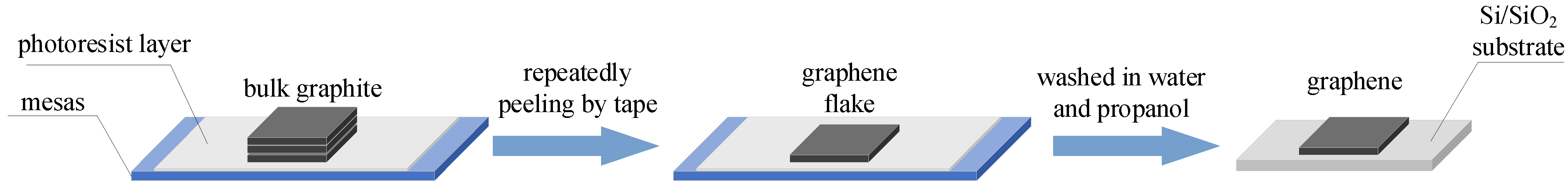

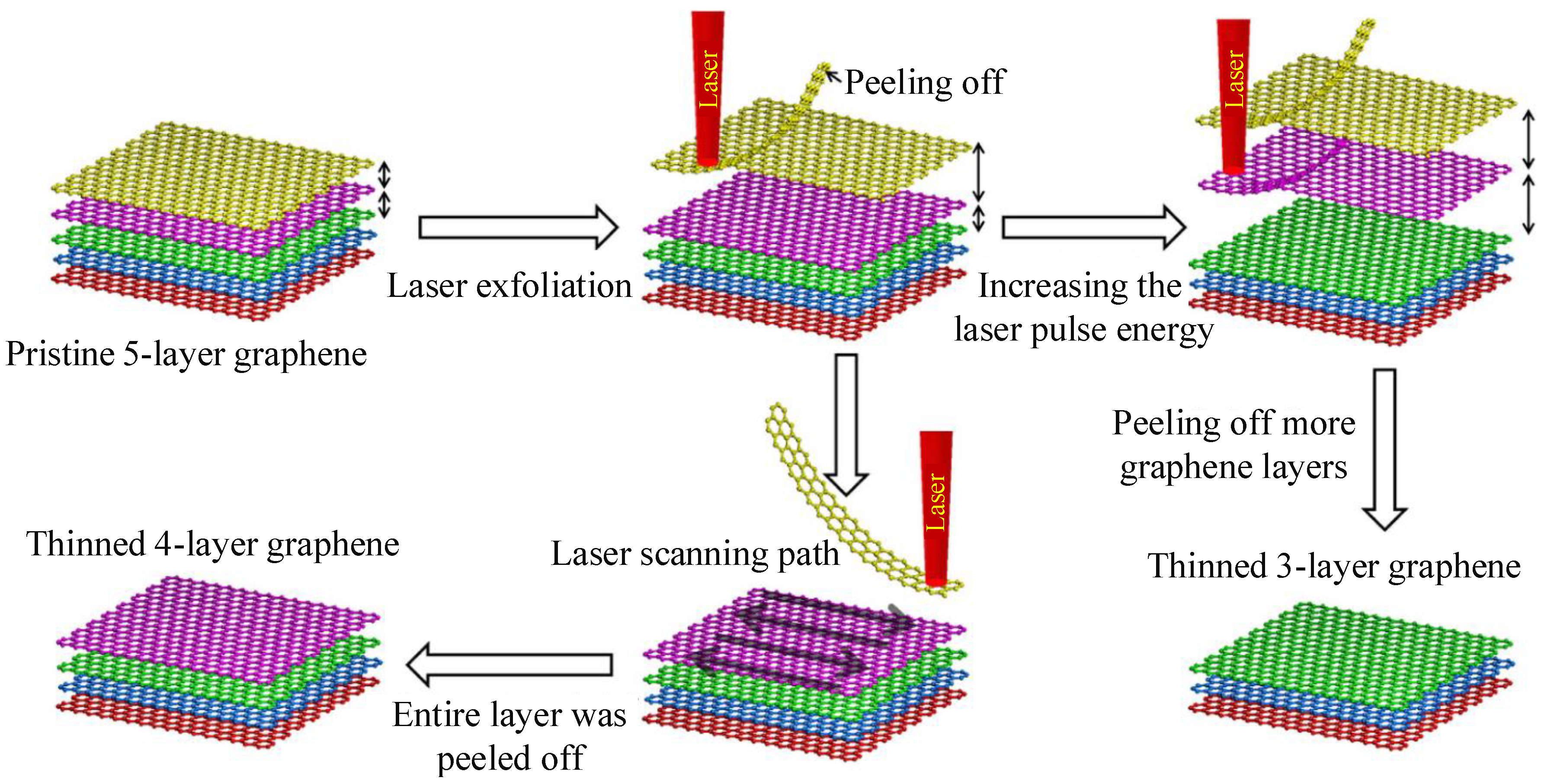


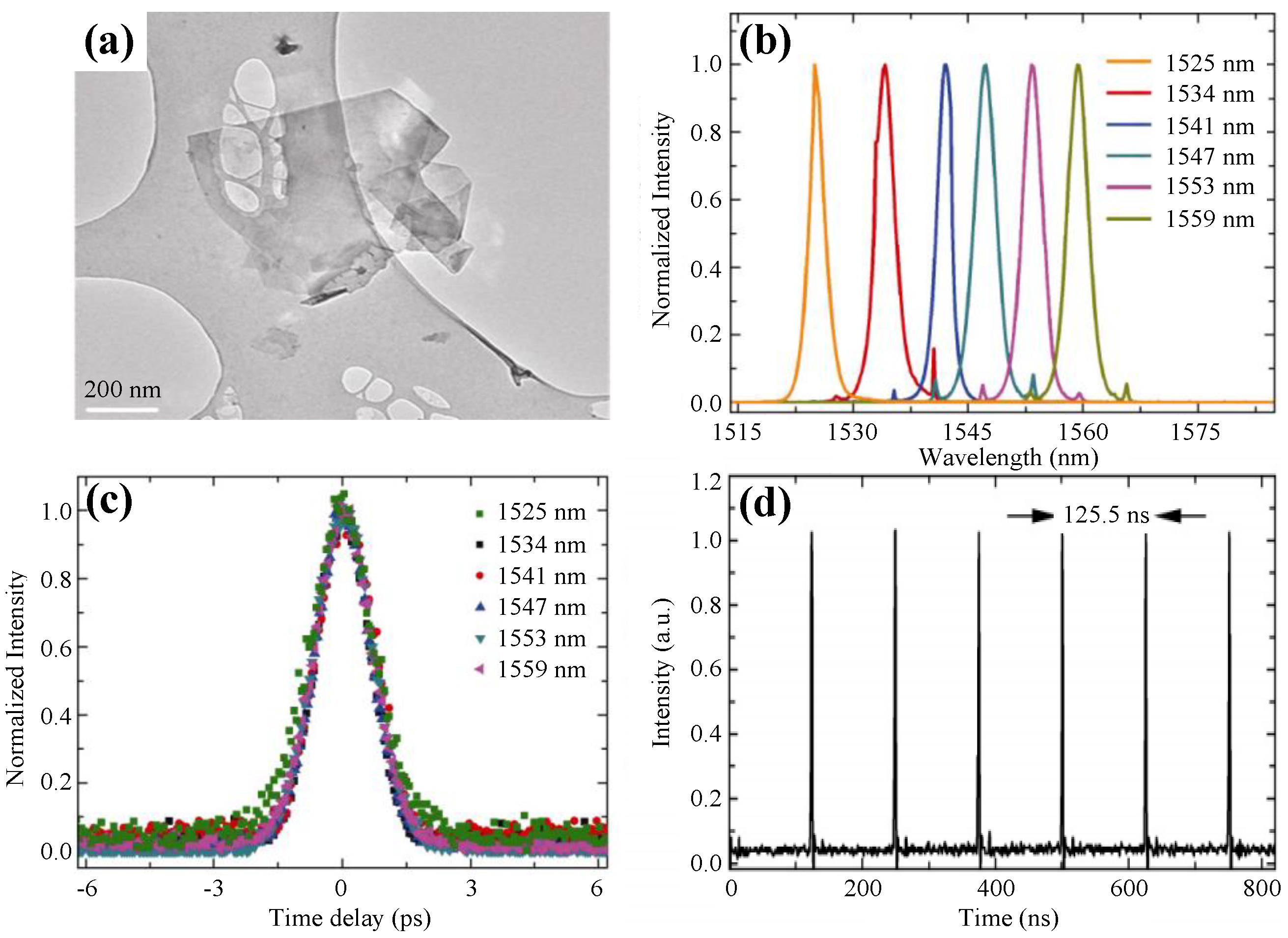
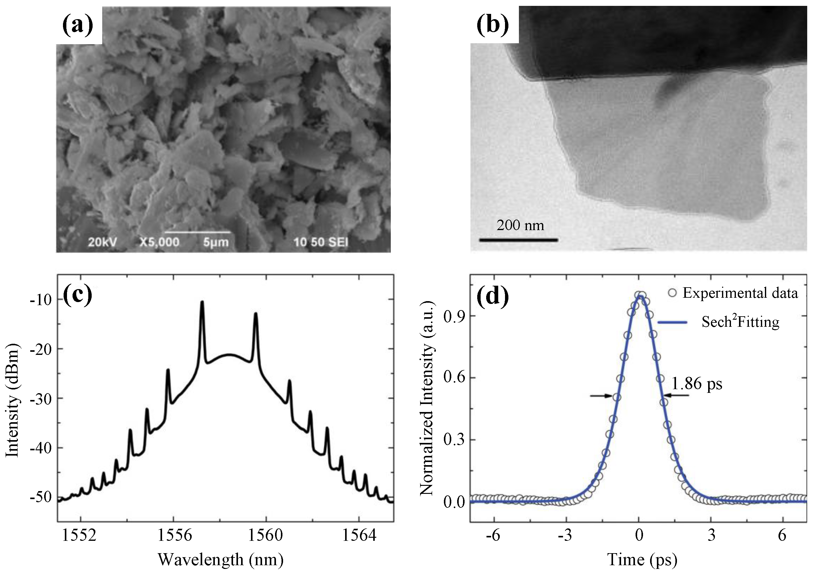


Publisher’s Note: MDPI stays neutral with regard to jurisdictional claims in published maps and institutional affiliations. |
© 2021 by the authors. Licensee MDPI, Basel, Switzerland. This article is an open access article distributed under the terms and conditions of the Creative Commons Attribution (CC BY) license (https://creativecommons.org/licenses/by/4.0/).
Share and Cite
Zhang, A.; Wang, Z.; Ouyang, H.; Lyu, W.; Sun, J.; Cheng, Y.; Fu, B. Recent Progress of Two-Dimensional Materials for Ultrafast Photonics. Nanomaterials 2021, 11, 1778. https://doi.org/10.3390/nano11071778
Zhang A, Wang Z, Ouyang H, Lyu W, Sun J, Cheng Y, Fu B. Recent Progress of Two-Dimensional Materials for Ultrafast Photonics. Nanomaterials. 2021; 11(7):1778. https://doi.org/10.3390/nano11071778
Chicago/Turabian StyleZhang, Aojie, Zihao Wang, Hao Ouyang, Wenhao Lyu, Jingxuan Sun, Yuan Cheng, and Bo Fu. 2021. "Recent Progress of Two-Dimensional Materials for Ultrafast Photonics" Nanomaterials 11, no. 7: 1778. https://doi.org/10.3390/nano11071778
APA StyleZhang, A., Wang, Z., Ouyang, H., Lyu, W., Sun, J., Cheng, Y., & Fu, B. (2021). Recent Progress of Two-Dimensional Materials for Ultrafast Photonics. Nanomaterials, 11(7), 1778. https://doi.org/10.3390/nano11071778