Abstract
A new, transparent, metal-free absorber, based on the use of multilayer graphene/dielectric laminates (GLs), is proposed for applications in the low-terahertz frequency range. The designed absorber has a total thickness of around 70 µm and consists of a front matching dielectric layer followed by a GL, a dielectric spacer and a back GL. The laminates are periodic structures constituted of graphene sheets separated by 50-nm-thick polyethylene terephthalate (PET) interlayers, while the matching layer and the spacer are one-quarter-wavelength thick and made of PET. The GLs are modeled as homogeneous-equivalent single layers (ESLs) characterized by their sheet resistances Rs. An innovative analytical method is proposed in order to select Rs values optimizing the electromagnetic wave absorption either in low-gigahertz or low-terahertz frequency range. The frequency spectra of the absorption, reflection and transmission coefficients are computed in the range up to 4 THz by using different values of Rs. Then, realistic Rs values of chemically doped graphene monolayers over PET substrates are considered. The designed absorbers are characterized by an absorption coefficient with a peak value of about 0.8 at the first resonant frequency of 1.1 THz, and a 1.4 THz bandwidth centered at 1.5 THz with reflection coefficient below - 10 dB. Moreover, the optical transmittance of the proposed absorbers are computed by means of the optical matrix theory and it is found to be greater than 86% in all the visible ranges.
1. Introduction
In the last decade, the exponential growth of wireless communications and data traffic has fueled the research in technologies operating at terahertz (THz) and low-THz frequency ranges [1]. Moreover, these technologies are attracting ever-growing interest in many other industrial and research fields, such as biomedical imaging and signal detection, as well as stealth materials and sensing [2]. Therefore, intensive efforts have been made to fabricate novel, transparent and multi-functional devices operating at such frequency regimes. In particular, the development of new absorbers operating in the low-THz and THz frequency range is generally recognized as an urgent challenge to be addressed, since high absorption is crucial for several applications such as modulators, sensors and solar cells [3,4]. Recently, resonance-based metamaterial absorbers have aroused intensive interest [5,6], since they can offer near unity absorption. However, the complexity of these structures leads to difficulties in fabrication because most of them employ metals, classified as critical raw materials and characterized by electrical and electromagnetic properties hardly tunable, especially when thin films are required [4,7]. Furthermore, most of these structures are not transparent in the visible frequency range, reducing their applications.
In this context, graphene, which is a two-dimensional honeycomb structure of carbon atoms, has gained a lot of interest due to its exceptional electrical, thermal, mechanical and optical properties [8]. Currently, two-dimensional graphene layers are characterized by optical transmittance greater than 90% (as a comparison, the Indium tin oxide transmittance is around 81%) and their conductivity can be tuned through electrical or chemical doping.
For instance, single-frequency, dual-frequency and wide-band absorbers made of graphene-based metasurfaces and characterized by large angle tolerance properties in the THz spectrum up to 4 THz are proposed in [3]. A tunable THz absorber employing a 5-nm-thick interlayer of Al2O3 is presented in [9] and an accurate procedure for the design of multilayer THz absorbers employing tunable graphene metamaterials has been developed in [10], with the aim of obtaining high absorption over a wide-THz frequency band. Moreover, in [11] tunable double-layer graphene wires are combined with metamaterials having unit cells of cross-shaped metallic resonator in order to realize a polarization-independent absorber with spectral tuning at THz frequency. Then, a hyperbolic metamaterial consisting of a multilayer structure of alternating graphene and Al2O3 layers on a CaF2 substrate is realized and characterized in [12]. More recently, a tunable ultra-broadband THz absorber based on two layers of graphene ribbons and two different kinds of substrate materials is proposed in [13] while an extensive study on broadband near-perfect absorbers consisting of single-layered and non-structured graphene loaded with periodical arrays of dielectric bricks is presented in [14]. Finally, in [15] a reliable method to extract the electromagnetic constitutive tensors of complex synthesized multilayer graphene-dielectric stacks in the terahertz band is derived.
Nevertheless, the realization of periodic graphene nanostructures is still not an easy task. Recently, Salisbury absorber screens, consisting of a thin resistive film, a dielectric spacer and a backside reflector, have attracted growing interest for the realization of graphene-based THz absorbers [7,13,14,15,16,17,18]. In fact, graphene films can act as resistive films [7] and, in addition, their conductivity can be tuned in order to obtain optimum absorption. For instance, numerical studies show that graphene ribbon arrays coupled with a graphene sheet can achieve a near unity absorption in a wide-THz bandwidth by changing graphene electrical properties through electrical doping due to an applied voltage [14,16]. A similar electrical doping has been investigated in [4,17]. Moreover, a new adaptive Salisbury absorbing screen providing a reflection coefficient lower than -10 dB in the frequency range 0.6–2.2 THz and with total thickness around 70 μm is proposed in [18]. The designed screen, backed by a perfect electrical conducting plate, consists of firstly a graphene layer acting as a lossy sheet and two spacers made of polyethylene terephthalate (PET), separated by an electrically tunable graphene/dielectric laminate (GL). Numerical analyses have been performed on the basis of the equivalent models and the results described in [19,20,21,22].
The objective of this paper is the design of new two-periods transparent metal-free absorbers made of multilayer graphene-PET laminates. The materials are chosen in order to obtain an optically transparent screen, and to avoid the use of metals or other critical raw materials, also for the backside reflector, which is usually made of a thin gold layer. The GLs are modelled as homogeneous-equivalent single layers (ESLs) characterized by proper sheet resistances, whose values are obtained analytically in order to achieve good absorption performances. The developed analytical method is innovative since it provides a simple and immediate tool that can be applied to design electromagnetic absorbers in the low-THz frequency range. Finally, the optical transmittances of the backside reflector and of the overall proposed absorbers are computed by means of the well-known matrix theory for the analysis of multilayer systems [23]. It results that the optical transmittance of the designed absorber is greater than 88% in all the visible ranges.
2. Absorber Structure
The schematic structure of the proposed graphene-based absorber is represented in Figure 1. The absorber consists of a front matching PET layer followed by a graphene/PET laminate L1, a PET spacer and a back graphene/PET laminate L2. The matching layer and the spacer have a one-quarter-wavelength thickness tsp; t1 and t2 are the thicknesses of the laminates L1 and L2, respectively.
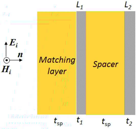
Figure 1.
Schematic structure of the cross-section of the planar absorber illuminated by a plane wave.
The absorber is assumed to have infinite transverse dimensions, and to be illuminated by a plane wave with normal incidence.
PET is selected for the realization of the spacer and matching layer due to its mechanical properties, optical transparency and cost-effectiveness. Moreover, graphene films over PET substrates are nowadays commercially available and they are characterized by outstanding electrical and mechanical properties [24]. Another polymer commonly used as substrate for graphene is polymethylmethacrylate (PMMA). However, PMMA films are characterized by worse mechanical properties than PET ones.
The ith laminate Li of Figure 2a consists of a periodic structure constituted of Ni bilayers made of a graphene sheet separated by a PET interlayer having thickness tint. Thus, the thickness of each graphene-PET bilayer is tb = δ + tint, δ being the graphene thickness, conventionally assumed equal to 0.34 nm. It results tb ≅ tint and the total thickness of the ith laminate, ti, is equal to Nitint.
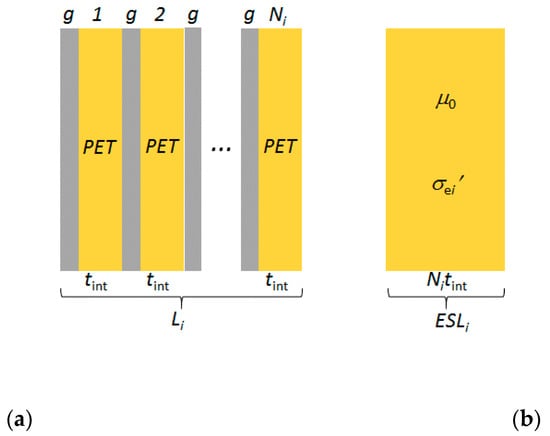
Figure 2.
Schematic structure of (a) graphene-polyethylene terephthalate (PET) laminate Li and (b) its equivalent single layer (ESLi).
3. Graphene and Polymer Modeling
3.1. Graphene Conductivity
The frequency-dependent conductivity σ(ω) of an isolated graphene sheet can be represented by Kubo’s formalism, which takes into account the intraband and the interband contributions [25].
In the low-THz frequency band only the intraband conductivity term is considered, since the interband one is negligible. In fact it results , i.e., , where μc is the chemical potential in eV, the reduced Planck’s constant (with h = 6.6262 × 10⁻³⁴ Js) and ω the angular frequency. It yields [25]:
in which e = 1.602 × 10⁻¹⁹ C is the elementary electron charge, kB = 1.38064 × 10⁻²³ J/K is the Boltzmann’s constant, T is the temperature in Kelvin and τ is the relaxation time of graphene.
It is worth noticing that if , i.e., if at T = 300 K, the exponential term in (1) becomes negligible and the intraband conductivity can be approximated by the following semi-classical Drude model:
where σ is the dc conductivity:
The scattering time can be expressed as a function of μc and of the carrier mobility μ in the following form [22]:
in which vF = 106 m/s is the Fermi velocity. Therefore, Equation (3) can be rewritten as:
The graphene dc conductivity σ at zero-field and zero-charge density is estimated to be close to the conductivity quantum 0.38 × 10⁻⁴ S and can reach the value of a few mS by increasing the chemical potential μc through chemical or electrical doping [24].
The graphene layers composing the GL are assumed to be decoupled electronically thanks to the presence of dielectric interlayers with a thickness in the order of some tens of nanometers. Moreover, due to the infinite planar dimensions of the homogeneous graphene monolayers, plasmonic surface waves are neglected [26,27].
3.2. Polymer Permittivity
The PET-frequency-dependent relative permittivity can be predicted by using the Havriliak–Negami model [28]:
where is the high-frequency value, the relaxation strength, the relaxation time and α and β fitting parameters. According to [29], the best fit with experimental data is obtained when = 2.54, = 0.46, = 0.05 ps, α = 2.9 and β = 0.9.
Thus, in the low-THz frequency range, the PET permittivity is a complex number, with a real part and an imaginary part , that are frequency-dependent quantities. It yields:
The frequency spectra of and are shown in Figure 3a,b in the range from 0.01 THz up to 4 THz.

Figure 3.
Frequency spectra of the (a) real and (b) imaginary part of the relative permittivity of PET polymer substrate.
3.3. Optical Transmittance of Graphene and PET Laminate
According to [30,31], the optical transmittance Topt λ = 550 nm at the light wavelength λ equal to 550 nm of stacked graphene monolayers is given by:
where N is number of suspended graphene layers and γ is the fine structure constant, equal to 1/137 [32]. Thus, for a single layer the optical transmittance is 97%, whereas for N = 4 or N = 5 it is 90% or 88%. However, such transmittance values do not consider the substrate effects that may not be neglected in case of graphene-based structures, like the ones sketched in Figure 1 and Figure 2a.
Indeed, the optical transmittance of GLs can be computed through the standard thin-film optics approach, based on the Fresnel equations [23]. For such calculations, a complex refractive index is typically assumed for graphene [33], with real part corresponding to the graphene refractive index and imaginary part representing the graphene extinction coefficient. It yields:
Very recent experiments have shown that in the visible range, is constant and equal to 3, while the graphene extinction coefficient is given by:
with ζ being a constant equal to 5.446 μm−1 and λ the incident light wavelength expressed in micrometers [34].
Concerning the dielectric layers, for a typical PET sample the complex refractive index is equal to the refractive index (a real number), since the PET extinction coefficient is zero in the visible range [35].
The graphene and PET refractive indices and extinction coefficients are reported in Figure 4a,b, respectively, for wavelengths ranging between 400 nm and 700 nm.
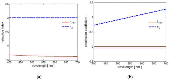
Figure 4.
Refractive index (a) and extinction coefficient (b) of graphene (- - -) and PET (―) in the visible range.
4. Transmission Wave Modeling
4.1. Multilayer Model
The overall transfer matrix [Φ] of the absorber structure sketched in Figure 1 is [19]:
in which [ΦLi] and [Φsp] are the transfer matrices of the ith laminate Li and of the PET layers (either the spacer or the front matching layer).
The transfer matrix [ΦLi] is given by:
where [Φgi] is the short-line transfer matrix of the ith single graphene layer with conductivity σi(ω):
and [Φint] is the transfer matrix of the PET dielectric interlayer:
The attenuation constant αint, the wavelength λS and the characteristic impedance ηS of the PET layers are respectively:
The transfer matrix [Φsp] of the PET spacer and matching layer is given by Equation (14) replacing αint with αsp = 2 πtsp/λS.
4.2. Equivalent Single-Layer Model of the Graphene-PET Laminate
In the low-THz frequency range, the PET interlayers with tint = 50 nm behave as short lines (SLs), since it results (tint/λs) << 1. Thus, the condition required to apply the homogenization procedure to the periodic structure given by the graphene-PET laminate of Figure 2a is satisfied [36]. Consequently, each multilayer laminate Li can be represented by the corresponding ESLi having thickness ti = Nitint, as shown in Figure 2b. The homogeneous ESLi is characterized by permeability μ0 and effective conductivity expressed in s/m [36], given by:
that can be rewritten as:
where the real and imaginary components, respectively and , are:
The transfer matrix [] of the homogeneous ESLi is:
where mi and ηi are the ESLi propagation constant and wave impedance, respectively given by:
Note that the ESLi behaves as an SL since (ti/λESLi) << 0.1 in the considered frequency range. The wavelength λESLi assumes the following new expression:
Thus, in the case of SL hypothesis, the ESLi transfer matrix expressed in Equation (22) becomes:
where σei(ω) is the equivalent effective conductivity, expressed in Siemens and computed as:
Considering Equation (18), the equivalent effective conductivity can be rewritten as:
4.3. Reflection, Transmission and Absorption Coefficients
The reflection R and transmission T coefficients of a multilayer absorber are given by the following expressions [18]:
in which Yin is the absorber input admittance:
and Φ11, Φ22, Φ12, Φ21 are the coefficients of the absorber overall transfer matrix (11). If the SL hypothesis (ti/λESLi ) << 0.1 is satisfied, the overall transfer matrix [Φ] can be computed using matrices [ΦESLi]SL instead of matrices [ΦLi] without losing accuracy.
Finally, the reflection coefficient in decibel RdB and the absorption coefficient A are obtained from R and T as:
5. Sheet Resistances of Graphene-PET Laminates
The absorption performances of the proposed transparent screens depend strongly on the laminate-sheet resistances that are functions of the number Ni and dc conductivity σi of the graphene layers. In order to obtain the optimum values of the sheet resistances, a new analytical formulation is developed on the basis of previously obtained results [37].
Each laminate Li is modeled as the corresponding homogeneous ESLi represented by the SL transfer matrix [ ΦESLi]SL expressed in Equation (26), in which the off-diagonal coefficients are and . Assuming the low-frequency hypothesis, the term can be neglected, being the total thickness of the ESLi in nanometric scale. Moreover, the equivalent effective conductivity in Equation (28) can be approximated with the term Niσi. Therefore, the transfer matrix [ ΦESLi]SL assumes the following simplified form.
where the sheet conductance Gsi can be written as:
The thickness of the spacer and matching layer sketched in Figure 1 is assumed equal to tsp = λsr/4 in which is the wavelength at the resonant frequency fr, being , the low-frequency PET permittivity. Therefore, the transfer matrix [Φsp]r at the resonance frequency assumes the following form:
in which . Thus, the overall transfer matrix at the resonant frequency [Φ]r is computed as:
The coefficients of matrix (37) are used to evaluate the corresponding input admittance Yinr and the transmission coefficient Tr. These quantities are expressed as functions of the sheet conductances Gs1 and Gs2. It yields:
Setting Yinr and Tr respectively equal to 1/η0 and T*, where T* is a target value of the transmission coefficient at frequency fr, it is possible to obtain the optimum laminate-sheet conductances. It yields:
with T* < 0.5. Notice that the latter equations can be used also in the low-gigahertz frequency range, as discussed in [37].
Considering a perfect electric conductor (PEC) back plate (i.e., Gs2 →∞) instead of a graphene-dielectric laminate, Equation (38) and Equation (39) become respectively:
Moreover, setting Yinr equal to 1/η0, the sheet conductance of the first laminate is obtained from Equation (42) as:
With the spacer thickness tsp being equal to λs/4, the peak values of the absorption coefficient occur at the following resonant frequency:
It should be noted that the low-frequency graphene conductivity and PET permittivity considered in the previous equations decrease in the low-THz frequency band. Thus, the values of sheet conductances given by Equations (40), (41) or (44) cannot be considered as the ones that optimize the absorption performances, but as initial reference values in the design process.
6. Optical Transmittance Modeling
The optical transmittance Topt of a material is defined as the ratio between the light intensity transmitted by the material to that incident upon it. The most general approach to compute Topt is based on a matrix formulation of the boundary conditions at the layer surfaces [23].
In case of a normally incident beam of light on a multilayer structure placed in air, the optical transmittance Topt can be computed as [38]:
where n0 is the air effective refractive index, conventionally equal to 1, and B and C are the normalized total tangential electric and magnetic fields at the front interface of the absorbing structure sketched in Figure 1 [23]. According to the optical matrix formulation, B and C are given by:
with [M] being the overall ray transfer matrix of the considered structure [23].
The ray transfer matrix [MLi] of the graphene laminate sketched in Figure 2a consisting of Ni graphene sheets separated by Ni PET interlayers is computed as:
where [Mg] and [Mint] are the ray transfer matrices of the graphene layer and of the PET interlayer. In particular, [Mg] is
With
being tg and () the conventional and the effective optical thickness of a graphene layer. Then, matrix [Mint] is obtained from Equations (49) and (50) replacing the graphene complex refractive index and thickness tg with the PET complex refractive index and thickness tint.
Finally, the overall ray transfer matrix [M] of the absorber structure sketched in Figure 1, is:
where matrix [Msp] of the PET spacer and matching layer is obtained from matrix [Mint] replacing tint with tsp.
7. Absorber Performance
The sheet conductances of the laminates L1 and L2 are computed by means of Equations (40) and (41) assuming εr = 3 and T* equal to 0.1, 0.07 and 0.05. The obtained values of the corresponding sheet resistances Rsi = 1/Gsi are reported in Table 1.

Table 1.
Sheet Resistances of Graphene-PET Laminates.
The reflection, transmission and absorption coefficients of the absorbers are computed in the frequency range 0.01–4 THz using Equations (29), (30), (32) and (33) combined with Equation (11). Each laminate Li is modeled through the ESLi-short-line transfer matrix of Equation (26) in which σei(ω) is given by Equation (28) where Niσi is the sheet conductance Gsi of the ith laminate. The scattering time τ and the spacer thickness tsp are assumed equal to 0.1 ps and 0.035 mm, respectively. The computed frequency spectra of R, T, A and RdB are represented in Figure 5 for different values of T*.
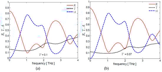
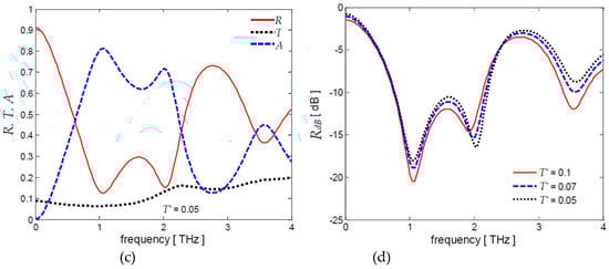
Figure 5.
Frequency spectra of (a–c) coefficients R, T, A and (d) RdB for τ = 0.1 ps, tsp = 0.035 mm and different values of T*.
It is worth noticing that the absorption coefficient A increases slowly as T* decreases and shows a peak value at 1.1 THz, i.e., the first resonant frequency, pretty close to 1.24 THz given by Equation (45) considering εr = 3. Furthermore, the transmission coefficient T at the resonant frequency assumes values close to the target values T*, i.e., 0.1, 0.07 and 0.05.
The previous calculations are carried out considering the laminate L2 as backside reflector. If the backside reflector is made of a PEC layer, i.e., if T* = 0 and Rs2 = 0, it yields Rs1 = 125 Ω/sq. The computed frequency spectra of coefficients R, T, A and of RdB are reported in Figure 6a,b. It is noticed that they are very similar to the ones shown in Figure 5 except for the increased peak value at second resonant frequency.
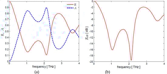
Figure 6.
Frequency spectra of coefficients (a) R,T,A and (b) RdB for τ = 0.1 ps, tsp = 0.035 mm in case of a perfect electric conductor (PEC) mirror layer, i.e., T* = 0.
For the sake of completeness, the input admittance Yin of the multilayer screen is computed by using Equation (31) with τ = 0.1 ps and tsp = 0.035 mm. The obtained frequency spectra of the real and imaginary parts of Yin are shown in Figure 7a,b for different values of T*.
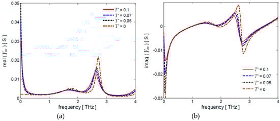
Figure 7.
Frequency spectra of the (a) real and (b) imaginary parts of the input admittance Yin for τ = 0.1 ps, tsp = 0.035 mm and different values of T*.
At a first resonance frequency of 1.1 THz the real and imaginary parts of Yin are equal to (1/η0) = 2.65 ms and zero, respectively, according to the optimal absorbance conditions assumed to obtain the analytical expressions of the sheet conductances.
It is interesting to compare the reflection coefficient computed when a PEC is considered as a backside reflector with the absorbance performance of the adaptive absorber described in [18]. This absorbing screen has a total thickness of 70 μm, it is backed by a PEC plate and it is made firstly of a graphene lossy sheet and of a multilayer graphene-silicon dioxide (SiO2) laminate, sandwiched between two PET dielectric layers. A reflection coefficient of -18 dB was obtained at about 1.1 THz when the graphene-SiO2 laminate was electrically doped by a 0.02 V/nm electrostatic field bias, giving rise to a laminate-sheet resistance of about 123 Ω/sq [18]. This value is very close to the one resulting from Equation (44) when the laminate L2 is replaced by a PEC layer.
The design of a feasible absorber requires the choice of doped graphene layers characterized by suitable values of sheet resistances in order to obtain laminates having effective sheet resistances close to the ones reported in Table 1. With this purpose, HNO3 chemically doped graphene layers, characterized by a dc conductivity of 8.33 ms and a sheet resistance of 120 Ω/sq [24], should be selected. In fact, values close to Rs1 = 135 ms and Rs2 = 31 ms corresponding to T* = 0.07 in Table 1 can be obtained using a single doped graphene layer in the first laminate L1 and four doped graphene layers in the back laminate L2.
The coefficients R, T, A and RdB of the designed absorber are computed assuming τ = 0.1 ps and tsp = 0.035 mm, as in the previous applications, and using the overall transfer matrix Equation (11) in which each laminate is represented by the multilayer (ML) matrix of Equation (12) or by the ESL-short-line matrix of Equation (26) obtained considering the sheet resistances of the doped graphene layers and the theoretical ones evaluated in the case T* = 0.07 (Table 1). The obtained results are shown in Figure 8a,b.
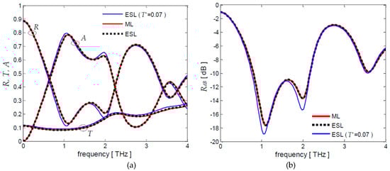
Figure 8.
Frequency spectra of coefficients (a) R, T, A and (b) RdB for the designed screen obtained using ML- and ESL-short-line models. As a comparison, the (a) R, T, A and (b) RdB frequency spectra obtained considering the theoretical sheet resistances obtained for T* = 0.07 (Table 1) are reported.
It can be noticed that the ML- and ESL-short-line spectra are practically coinciding and they are very close to the ones computed by using the theoretical sheet resistance values. Furthermore, the designed absorber has a 1.4 THz bandwidth centered at 1.5 THz with a reflection coefficient below −10 dB.
Finally, a sensitivity analysis of the absorption coefficient A is carried out for T* = 0.07 with respect to different values of tsp and of τ, setting respectively τ = 0.1 ps or tsp = 0.035 mm. The obtained frequency spectra are represented in Figure 9a,b.
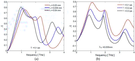
Figure 9.
Frequency spectra of absorber coefficient A for T* = 0.07 setting (a) τ = 0.1 ps and (b) tsp = 0.035 mm.
The first resonance frequency in Figure 9a is between 0.9 THz and 1.28 THz, depending on the spacer thickness ranging between 0.03 mm and 0.04 mm. The influence of the scattering time on the frequency spectra is noticeable in Figure 9b, showing very different peak values and resonance frequencies for small changes of τ. In fact, the frequency dependence of graphene conductivity is more evident as the scattering time increases. These results highlight the importance of an accurate estimation of the scattering time, that is indicative of the graphene quality since it is strictly related to the carrier mobility and chemical potential [21].
8. Absorber Transparency
The optical transmittance Topt of the absorber structure sketched in Figure 1 is computed by means of Equation (46), considering the back laminate transfer matrix [ML2] or the overall matrix [M], respectively given by Equations (48) and (51). In particular, a sensitivity analysis of Topt with respect to the number of graphene layers N2 of the back laminate L2 and to the interlayer thickness tint is carried out. Figure 10a shows Topt spectra of the back laminate having tint = 50 nm and N2 ranging between 2 and 5, while Figure 10b reports Topt spectra of the corresponding overall structures, i.e., also considering the matching layer, the laminate L1 and the spacer. On the other hand, Figure 10c reports Topt spectra of the back laminate consisting of five doped graphene layers (N2 = 5) and interlayer thickness tint varying from 50 nm to 200 nm. Similarly, Figure 10d shows Topt of the corresponding overall structures, i.e., also considering the matching layer, the laminate L1 and the spacer.
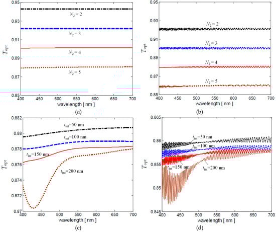
Figure 10.
Optical transmittance Topt of the (a,c) back laminate L2 and (b,d) of the overall absorbing structure. The spectra are computed in the visible range considering tint = 50 mm and N2 ranges between 2 and 5 (a,b) or N2 = 5 and tint varying from 50 nm to 200 nm (c,d).
It can be noticed that Topt is always greater than 85%. Moreover, when the PET interlayer thickness is one order of magnitude lower than the considered wavelength, Topt can be easily computed by means of the approximated expression Equation (8). As the PET interlayer thickness increases, Topt cannot be computed by means of Equation (8), as shown in Figure 10c. In fact, mutual reflections inside the interlayer are no more than negligible.
Finally, from Figure 10b it results that Topt of the designed screen (with N2 = 4) is around 88% in all the visible ranges.
9. Conclusions
The proposed absorber structure consists of a front matching PET layer followed by a graphene/PET laminate, a PET spacer and a back graphene/PET laminate. The matching layer and the spacer have one-quarter-wavelength thickness. The structure is extremely simple since it does not include complex frequency-selective surfaces or metamaterials. Moreover, the designed absorbers have a total thickness of 70 µm and they are transparent and metal free, since no metal is used, also for the backside reflector.
The absorption performances are evaluated through numerical calculations in the low-terahertz frequency range and both graphene conductivity and PET permittivity are considered as frequency-dependent quantities. A homogenization procedure is applied to represent the periodic graphene-PET structures as equivalent short-line single layers.
The optimum sheet resistances of the laminates are obtained analytically as functions of the interlayer relative permittivity and of the target transmission coefficient at the first resonance frequency. It is worth noticing that the analytical expressions of the optimum laminate-sheet resistances can be applied to both low-gigahertz or low-terahertz frequency ranges. Then, HNO3 chemically doped graphene layers are considered in order to design feasible absorbing screens with laminate-sheet resistances comparable with the theoretical ones. The computed frequency spectra of the absorption, reflection and transmission coefficients in the frequency range up to 4 THz prove the good performance of the designed absorbers and the utility of the proposed design method. In particular, the proposed screen has a 1.4 THz bandwidth centered at 1.5 THz with reflection coefficients below - 10 dB and an absorption coefficient with peak values around 0.8 at the first resonant frequency of 1.1 THz. Then, a sensitivity analysis is carried out to highlight the strong influence of the estimated scattering time on the screen performances.
Finally, the optical transmittance of the proposed absorber is computed by means of the optical matrix theory and we conclude that such transmittance is greater than 88% in all the visible ranges.
Author Contributions
Conceptualization, methodology, validation, formal analysis, investigation, writing, review and editing, A.G.D., M.D., M.S.S.; software, A.G.D. All authors have read and agreed to the published version of the manuscript.
Funding
This research received no external funding.
Acknowledgments
The authors thank Francesca Sarto (ENEA) for technical discussions about optical transmittance calculations.
Conflicts of Interest
The authors declare no conflict of interest.
References
- Nagatsuma, T.; Ducournau, G.; Renaud, C.C. Advances in terahertz communications accelerated by photonics. Nat. Photonics 2016, 10, 371. [Google Scholar] [CrossRef]
- Song, H.J.; Nagatsuma, T. Present and future of terahertz communications. IEEE Trans. Terahertz Sci. Technol. 2011, 1, 256–263. [Google Scholar] [CrossRef]
- Chen, M.; Sun, W.; Cai, J.; Chang, L.; Xiao, X. Frequency-tunable terahertz absorbers based on graphene metasurface. Opt. Commun. 2017, 382, 144–150. [Google Scholar] [CrossRef]
- Wang, Y.; Song, M.; Pu, M.; Gu, Y.; Hu, C.; Zhao, Z.; Wang, C.; Yu, H.; Luo, X. Staked graphene for tunable terahertz absorber with customized bandwidth. Plasmonics 2016, 11, 1201–1206. [Google Scholar] [CrossRef]
- Landy, N.I.; Sajuyigbe, S.; Mock, J.J.; Smith, D.R.; Padilla, W.J. Perfect metamaterial absorber. Phys. Rev. Lett. 2008, 100, 207402. [Google Scholar] [CrossRef]
- Watts, C.M.; Liu, X.; Padilla, W.J. Metamaterial electromagnetic wave absorbers. Adv. Mater. 2012, 24, OP98–OP120. [Google Scholar] [CrossRef]
- Min Woo, J.; Kim, M.S.; Woong Kim, H.; Jang, J.H. Graphene based salisbury screen for terahertz absorber. Appl. Phys. Lett. 2014, 104, 081106. [Google Scholar] [CrossRef]
- Baringhaus, J.; Ruan, M.; Edler, F.; Tejeda, A.; Sicot, M.; Taleb-Ibrahimi, A.; Li, A.-P.; Jiang, Z.; Conrad, E.H.; Tegenkamp, C.; et al. Exceptional ballistic transport in epitaxial graphene nanoribbons. Nature 2014, 506, 349–354. [Google Scholar] [CrossRef]
- Faraji, M.; Moravvej-Farshi, M.K.; Yousefi, L. Tunable THz perfect absorber using graphene-based metamaterials. Opt. Commun. 2015, 355, 352–355. [Google Scholar] [CrossRef]
- Fardoost, A.; Vanani, F.G.; Amirhosseini, A.A.; Safian, R. Design of a multilayer graphene-based ultrawideband terahertz absorber. IEEE Trans. Nanotechnol. 2016, 16, 68–74. [Google Scholar]
- Zhang, Y.; Feng, Y.; Zhu, B.; Zhao, J.; Jiang, T. Graphene based tunable metamaterial absorber and polarization modulation in terahertz frequency. Opt. Express 2014, 22, 22743–22752. [Google Scholar] [CrossRef] [PubMed]
- Chang, Y.C.; Liu, C.H.; Liu, C.H.; Zhang, S.; Marder, S.R.; Narimanov, E.E.; Zhong, Z.; Norris, T.B. Realization of mid-infrared graphene hyperbolic metamaterials. Nat. Commun. 2016, 7, 1–7. [Google Scholar] [CrossRef] [PubMed]
- Daraei, O.M.; Goudarzi, K.; Bemani, M. A tunable ultra-broadband terahertz absorber based on two layers of graphene ribbons. Opt. Laser Technol. 2020, 122, 105853. [Google Scholar] [CrossRef]
- Soleymani, A.; Meymand, R.E.; Granpayeh, N. Broadband near-perfect terahertz absorber in single-layered and non-structured graphene loaded with dielectrics. Appl. Opt. 2020, 59, 2839–2848. [Google Scholar] [CrossRef]
- Aladadi, Y.T.; Alkanhal, M.A.S. Extraction of the terahertz constitutive tensors of multilayer graphene-dielectric stacks. Opt. Commun. 2020, 464, 125487. [Google Scholar] [CrossRef]
- Xing, R.; Dong, C.; Zhu, B.; Gao, Y.; Jian, S. Numerical analysis on ribbon-array-sheet coupled graphene terahertz absorber. IEEE Photonics Technol. Lett. 2016, 28, 2207–2210. [Google Scholar] [CrossRef]
- Dong, Y.; Liu, P.; Yu, D.; Li, G.; Yang, L. A tunable ultrabroadband ultrathin terahertz absorber using graphene stacks. IEEE Antennas Wirel. Propag. Lett. 2016, 16, 1115–1118. [Google Scholar] [CrossRef]
- D’Aloia, A.G.; D’Amore, M.; Sarto, M.S. Adaptive terahertz absorber based on tunable graphene multilayer. In Proceedings of the 2017 International Symposium on Electromagnetic Compatibility-EMC EUROPE, Angers, France, 4–7 September 2017; pp. 1–6. [Google Scholar]
- D’Aloia, A.G.; D’Amore, M.; Sarto, M.S. Terahertz Shielding Prediction of Id-Periodic N Anolayered Coatings by an Effective Homogeneous Model. In Proceedings of the 2018 International Symposium on Electromagnetic Compatibility (EMC EUROPE), Amsterdam, The Netherlands, 27–30 August 2018; pp. 772–777. [Google Scholar]
- D’Amore, M.; D’Aloia, A.G.; Sarto, M.S. Terahertz shielding effectiveness and optical transmittance of graphene multilayer thin sheets. In Proceedings of the 2014 International Symposium on Electromagnetic Compatibility, Gothenburg, Sweden, 1–4 September 2014; pp. 482–487. [Google Scholar]
- D’Aloia, A.G.; D’Amore, M.; Sarto, M.S. Terahertz shielding effectiveness of graphene-based multilayer screens controlled by electric field bias in a reverberating environment. IEEE Trans. Terahertz Sci. Technol. 2015, 5, 628–636. [Google Scholar] [CrossRef]
- D’Aloia, A.G.; D’Amore, M.; Sarto, M.S. Optimal terahertz shielding performances of flexible multilayer screens based on chemically doped graphene on polymer substrate. In Proceedings of the 2015 IEEE International Symposium on Electromagnetic Compatibility (EMC), Gothenburg, Sweden, 1–4 September 2014; pp. 1030–1035. [Google Scholar]
- Macleod, H.A. Thin-Film Optical Filters; CRC press: Boca Raton, FL, USA, 2010. [Google Scholar]
- Bae, S.; Kim, H.; Lee, Y.; Xu, X.; Park, J.S.; Zheng, Y.; Lei, T.; Kim, H.R.; Kim, K.S.; Kim, Y.J.; et al. Roll-to-roll production of 30-inch graphene films for transparent electrodes. Nat. Nanotechnol. 2010, 5, 574. [Google Scholar] [CrossRef]
- Hanson, G.W. Dyadic Green’s functions for an anisotropic, non-local model of biased graphene. IEEE Trans. Antennas Propag. 2008, 56, 747–757. [Google Scholar] [CrossRef]
- Ju, L.; Geng, B.; Horng, J.; Girit, C.; Martin, M.; Hao, Z.; Bechtel, H.A.; Liang, X.; Zettle, A.; Wang, F.; et al. Graphene plasmonics for tunable terahertz metamaterials. Nat. Nanotechnol. 2011, 6, 630. [Google Scholar] [CrossRef]
- Jablan, M.; Buljan, H.; Soljacic, M. Plasmonics in graphene at infrared frequencies. Phys. Rev. B 2009, 80, 245435. [Google Scholar] [CrossRef]
- Havriliak, S.; Negami, S. A complex plane representation of dielectric and mechanical relaxation processes in some polymers. Polymer 1967, 8, 161–210. [Google Scholar] [CrossRef]
- Fedulova, E.V.; Nazarov, M.M.; Angeluts, A.A.; Kitai, M.S.; Sokolov, V.I.; Shkurinov, A.P. Studying of dielectric properties of polymers in the terahertz frequency range. In Saratov Fall Meeting 2011: Optical Technologies in Biophysics and Medicine XIII.; International Society for Optics and Photonics: Saratov, Russia, 2012; p. 83370I. [Google Scholar]
- Kang, M.H.; Milne, W.I.; Cole, M.T. Doping stability and opto-electronic performance of chemical vapour deposited graphene on transparent flexible substrates. IET Circuits Devices Syst. 2015, 9, 39–45. [Google Scholar] [CrossRef]
- Dawlaty, J.M.; Shivaraman, S.; Strait, J.; George, P.; Chandrashekhar, M.; Rana, F.; Spencer, M.G.; Veksler, D.; Chen, Y. Measurement of the optical absorption spectra of epitaxial graphene from terahertz to visible. Appl. Phys. Lett. 2008, 93, 131905. [Google Scholar] [CrossRef]
- Nair, R.R.; Blake, P.; Grigorenko, A.N.; Novoselov, K.S.; Booth, T.J.; Stauber, T.; Peres, N.M.R.; Geim, A.K. Fine structure constant defines visual transparency of graphene. Science 2008, 320, 1308. [Google Scholar] [CrossRef]
- Blake, P.; Hill, E.; Castro Neto, A.H.; Novoselov, K.S.; Jiang, D.; Yang, R.; Booth, T.J.; Geim, A.K. Making graphene visible. Appl. Phys. Lett. 2007, 91, 063124. [Google Scholar] [CrossRef]
- Bruna, M.; Borini, S. Optical constants of graphene layers in the visible range. Appl. Phys. Lett. 2009, 94, 031901. [Google Scholar] [CrossRef]
- Elman, J.F.; Greener, J.; Herzinger, C.M.; Johs, B. Characterization of biaxially-stretched plastic films by generalized ellipsometry. Thin Solid Films 1998, 313, 814–818. [Google Scholar] [CrossRef]
- D’Aloia, A.G.; D’Amore, M.; Sarto, M.S. Effective medium model of periodic nanolayered transparent shields. IEEE Trans. Electromagn. Compat. 2019, 61, 1803–1810. [Google Scholar] [CrossRef]
- D’Aloia, A.G.; D’Amore, M.; Sarto, M.S. Transparent Graphene-Based Absorber for Next Generation Wireless 5G Technology. In Proceedings of the 2019 International Symposium on Electromagnetic Compatibility-EMC EUROPE, Barcelona, Spain, 2–6 September 2019; pp. 360–365. [Google Scholar]
- Dobrowolski, J.A. Optical properties of films and coatings. Handb. Opt. I 1995, 42, 3–130. [Google Scholar]
© 2020 by the authors. Licensee MDPI, Basel, Switzerland. This article is an open access article distributed under the terms and conditions of the Creative Commons Attribution (CC BY) license (http://creativecommons.org/licenses/by/4.0/).