Abstract
In this paper, a novel, GaN-based high electron mobility transistor (HEMT) using an ultra-thin barrier (UTB) with a local charge compensation trench (LCCT) is designed and optimized. Because the negative plasma-etching process, as well as the relaxing lattice during the process would introduce equivalent negative charges into the under-LCCT region, the electron will be partially squeezed out from this area. The electric field (E-field) around this region will therefore redistribute smoothly. Owing to this, the proposed LCCT-HEMT performs better in power applications. According to the simulation that is calibrated by the experimental data, the Baliga’s figure of merits (BFOM) of LCCT-HEMT is around two times higher than that of the conventional UTB-HEMT, hinting at the promising potential of proposed HEMT.
1. Introduction
Because of the polarization effect in the AlGaN/GaN heterojunction, a high-density two-dimensional electron gas (2DEG) could be induced by properly modulating the heterojunction parameters, such as the Aluminum mole-fraction and the AlGaN thickness [1]. Such 2DEG in the AlGaN/GaN heterojunction features high-current transportation capability and high response speed to the electric field (E-field). These advantages put forth a class of electron devices—high electron mobility transistors (HEMTs), which are being extensively studied and considered as the promising candidates in next-generation power and high-frequency applications [2,3,4]. After the successful development of AlGaN/GaN enhancement-type HEMTs, these HEMTs immediately attracted a lot of attention [5,6,7,8,9,10]. More inspiringly, two approaches—both the p-type gate and cascaded Si-GaN transistors—have already been successfully commercialized [11]. However, they face many formidable challenges in practice, such as relatively low stability in high bias and a weak level of integration [12,13,14]. To solve these problems, researchers have been focused on designing new device structures to realize the enhancement type without introducing extra side-effects.
In this sense, F-ion implantation [5], the dual-channel recessed Metal-Insulator-Semiconductor Field Effect Transistor (MISFET) [15], and Field-coupled High Electron Mobility Transistor (HEMT) [16] have been developed and analyzed thoroughly. In the meantime, a low-density drain (LDD) technique has been proposed, and can be introduced into these novel lateral device structures to further balance the turn-on resistance (Ron) with the breakdown voltage (BV) [17,18]. In other words, this LDD could be used to enhance the device’s Baliga Figure-of-Merits (BFOM) in a form that has been adopted in recent GaN power device research and is depicted in Equation (1), where BV is the breakdown voltage and is the on-state resistance [19,20]:
Nevertheless, to redistribute the E-field, LDD requires etching or an ion implantation process to form a special alloy barrier region which is beside the gate to modulate the 2DEG density underneath. This process always causes lattice damages and, hereby, low electron mobility [8,15,21]. Fortunately, a novel HEMT architecture that utilizes the charge compensation from the Silicon Nitride (SiN) to the AlGaN ultra-thin barrier (UTB) has been presented [22,23]. In this architecture, one can modulate the concentration of 2DEG induced in an AlGaN/GaN interface without etching the barrier just by adding or removing the SiN layer which supplies the compensation charges. In other words, to realize the enhancement-type HEMT, one can partially remove the SiN on the UTB at which the gate metal will be deposited. Therefore, by such virtue of UTB, a LDD-like technique could be introduced naturally into the HEMT without lowering the quality of the heterojunction. Furthermore, recent experiment results have already demonstrated the prospect of UTB-HEMT in power applications [24,25].
In this paper, we proposed a novel UTB HEMT with a local charge compensation trench (LCCT) to further improve the performance of AlGaN/GaN HEMT. Such LCCT-HEMT avoids the lattice damage in the barrier, and in the meantime, LCCT could modulate the 2DEG concentration to smoothen the reverse E-field by introducing extra negative charges [26,27]. In this way, BFOM that is two times higher, compared with conventional UTB HEMT, could be obtained in the proposed device with a properly designed LCCT according to simulation that is calibrated by experimental data. These results reveal the potential of proposed HEMT in high-power applications.
2. Device Setup and Mechanism
The proposed HEMT device was generated on a conventional GaN-on-Silicon wafer with an AlGaN/GaN heterojunction on the top. The configuration details of this wafer can be found in Reference [22] and also in Figure 1a.
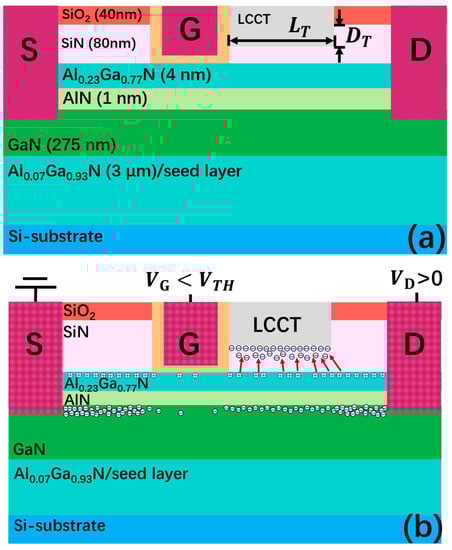
Figure 1.
The schematic (a) cross-section of proposed high-electron-mobility transistor with a local charge compensation trench (LCCT-HEMT) and (b) illustration of local charge compensation (red arrow represents electric field (E-field)).
The specification of the proposed device is listed in Table 1. It should be noted that besides the conventional source, drain, and gate, the device owns a special LCCT just adjacent to the gate. This LCCT could be formed by a typical etching process during which the ion bombardment injects extra negative charges into the Silicon Nitride (SiN). In the meantime, the recessed SiN relieves piezoelectric stress itself, leading to a further reduction of polarization charges in AlGaN. This procedure brings equally more negative charges into the SiN, whereas the precise negative charge distribution in SiN layer is hard to tell. However, the etching speed can be stabilized properly, which means the negative charge is introduced at a constant speed with a constant introducing rate. Thus, for simplification, a uniform distribution of such charges is assumed in this research, which is reasonable according to the Reference [26] but still requires further study. Besides, other charges and trap settings in each layer could be found in the original works of UTB-HEMT, extracted from experiments [22,23].

Table 1.
Device specifications.
The fabrication process of the proposed LCCT-HEMT is schematically depicted in Figure 2. The whole procedure could commence with a UTB wafer. Thereafter, the ohmic contacts could be formed by the physical vapor deposition (PVD), followed by the gate etching process. Here, the etching rate of the AlGaN barrier could be easily distinguished from the rate of SiN passivation layer, meaning the etching hurt could be minimized by properly designing the etching recipe. Then, the gate dielectric and gate metal could be deposited by atomic layer deposition (ALD) and PVD, respectively. Finally, the LCCT could be fabricated by elaborately etching the passivation layer to introduce the negative charges. Furthermore, some other materials that could introduce negative charges into the structure, such as ALD-grown oxide, could alternatively be chosen.
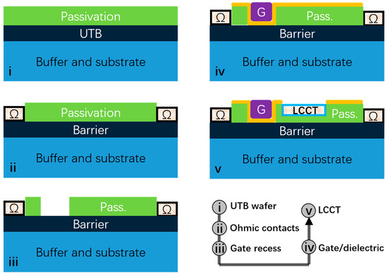
Figure 2.
The E-field distribution along the channel in LCCT-HEMT when the drain voltage is 800 V.
In this sense, compared with the conventional UTB HEMT, the proposed LCCT-HEMT exhibits the capability of E-field redistribution in a high drain bias, thus enabling higher BV of the device, as shown in Figure 3a,b. Furthermore, a longer and/or deeper LCCT offers higher capability of E-field redistribution, resulting in a smoother depletion region and higher BV, as shown in Figure 3c.
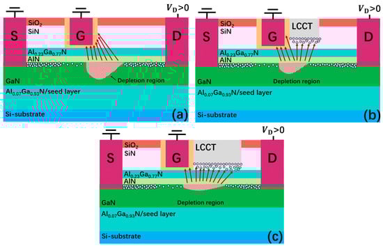
Figure 3.
The schematic charges and electric field distribution of (a) conventional ultra-thin barrier HEMT (UTB-HEMT), (b) LCCT-HEMT with a short LCCT, and (c) LCCT-HEMT with a longer and deeper LCCT (red arrow represents electric field).
As shown in Figure 1b, the recessed LCCT exerts two main effects. The first one is that, as mentioned above, the LCCT relieves the stress of the AlGaN layer, turning out a reduction of the polarization charges; whereas the other one, which has been depicted before as well, is that negative charges are introduced into the remaining SiN during the formation of the LCCT, which attracts the E-field generated from the positive polarization charge and as a result, partially squeezes out 2DEG underneath.
This functionality of LCCT could be illustrated explicitly by simulations as well. As shown in Figure 4, the conduction band of conventional HEMT only with a thin AlGaN barrier is higher than that of the device with SiN passivation. In addition, as aforementioned, the LCCT could gently lift the band structure by introducing the negative charges and partially canceling out the polarization.
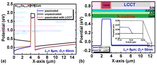
Figure 4.
The simulated conduction band structure (a) perpendicular to the wafer through the LCCT region and (b) along the two-dimensional electron gas (2DEG) channel of conventional HEMT, UTB-HEMT, and LCCT-HEMT.
Besides, before all detailed investigations, the Silvaco-ATLAS simulator, models, and corresponding settings were verified with the experimental data from previous UTB-HEMT works. The simulation models used in ATLAS were the Shockley-Read-Hall (SRH) recombination model, Fermi-Dirac statistic model, and the parallel electric field dependence model. The calibration commenced with the establishment of the device structure, which is strictly generated in ATLAS with the same geometry parameters of the experimental one. Then, the calibration is done by revising the polarization parameters, such as charge density and relaxation degree. As shown in Figure 5, the voltage–current curves match well not only regarding linear region, but also the subthreshold region, indicating the settings of simulation are reasonable. Furthermore, the breakdown voltage in simulation is adjusted to the value of the experiment, which is around 1200 V and omitted in these figures. Thus, this suggests the simulation is accurate and reasonable.
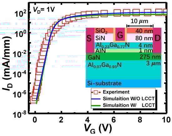
Figure 5.
The calibration of the simulator with the experiments (inset figure is the structure used in the calibration).
3. Result and Discussion
Figure 6 shows the output characteristics of the proposed device with a different depth and length, respectively. As seen in Figure 6, LCCT does impose the device current by modulating the fixed charge in SiN which will repel the 2DEG under LCCT. As a result, with the increasing depth and length, on-state resistance increases from around 9 Ω·mm to around 15 Ω·mm. However, it should be noted that in order to maintain the polarization charges introduced by LPCVD-SiN and avoid hurting the AlGaN lattice, the depth of LCCT should not exceed 75 nm.
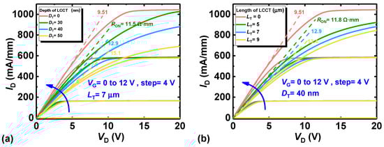
Figure 6.
The output characteristics of the proposed LCCT-HEMT with different (a) LCCT depth and (b) LCCT length.
Figure 7 shows the extracted on-resistance and corresponding BV, respectively. As shown in Figure 7a,b, the resistance and BV of LCCT-HEMT increase with longer and deeper LCCT. When the LCCT depth reaches 70 nm, which means that the thickness of the remaining LPCVD-SiN under LCCT is only 10 nm, the charge modulated by LCCT repels the 2DEG heavily, making the resistance increase dramatically. Figure 7c shows the calculated BFOM of the LCCT-HEMT in comparison with that of UTB-HEMT. The BFOM firstly grows with the increasement of LCCT depth and then drops after the depth of LCCT is deeper than 40 nm. A peak BFOM of 281 kW/mm is achieved when the length reaches 9.2 µm and the depth reaches 40 nm. Compared with the BFOM of the conventional UTB-HEMT, which is about 142 KV/mm, the proposed LCCT- HEMT performs almost two times better in terms of the BFOM.
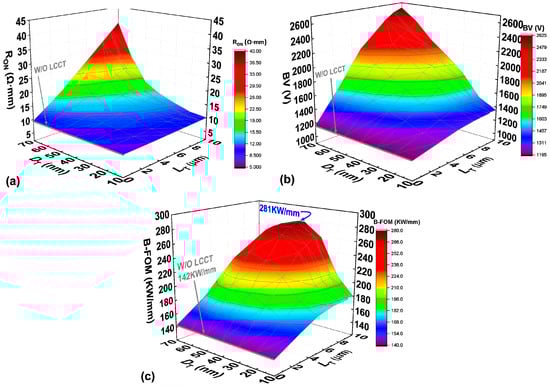
Figure 7.
The extracted (a) on-resistance, (b) corresponding breakdown voltage (BV), and (c) Baliga Figure-of-Merits (BFOM) of proposed LCCT-HEMT with different LCCT configurations.
Such an improvement was achieved by the suppression of the high E-field under the gate, provided by LCCT. In the “off” state, owing to the charges introduced by LCCT, the E-field around the gate redistributes into a smooth form, as shown in Figure 8. As a result, the E-field targeting to the gate is suppressed, and hereby, the BV increases effectively. Specifically, when the drain voltage is at 800 V, the LCCT reduces the E-field concentration around gate (see red region in Figure 8). That is, when the LCCT depth is 30 nm in Figure 8b, the charge introduced by LCCT is not strong enough to redistribute the E-field. On the contrary, when the depth is 50 nm, the charge is effective enough to suppress the E-field around the gate, which is shown in Figure 8c,d. Simultaneously, the leakage current is constricted greatly by the long and deep LCCT when the drain voltage is at 800V, as shown in Figure 9.
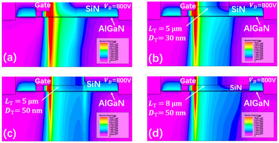
Figure 8.
The simulated E-field distribution in (a) conventional UTB-HEMT, and (b–d) LCCT-HEMT with different LCCT configurations when the drain voltage is 800 V.
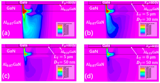
Figure 9.
The simulated current density distribution in (a) conventional UTB-HEMT, and (b–d) LCCT-HEMT with different LCCT configurations when the drain voltage is 800 V.
Additionally, the E-field distribution along the channel is presented in Figure 10 to further demonstrate the LCCT effects. As seen in Figure 10, a maximum E-field reduction of 2.8 MV/cm was achieved by optimizing LCCT configuration. Apparently, the E-field distribution along the channel in LCCT-HEMT is smoother than that in UTB-HEMT, which is consistent with the mechanism demonstrated in Section 2. Therefore, by optimizing the LCCT length and the depth, the proposed HEMT could exhibit better performance in power applications. However, notably, the precise parameters of LCCT depends on the process, which suggests that exclusive experiments are required in future studies.
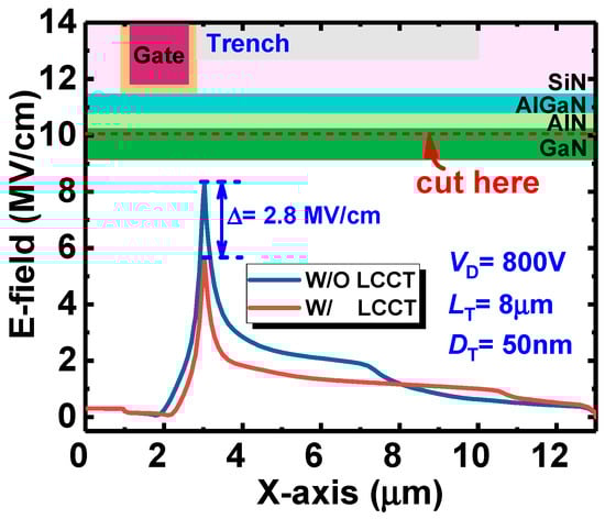
Figure 10.
The E-field distribution along the channel in LCCT-HEMT when the drain voltage is 800 V.
4. Conclusion
In this paper, a novel, ultra-thin-barrier HEMT with LCCT was proposed and investigated via the experimentally calibrated simulator, ATLAS. Proved by the detailed analysis and simulation, it is the E-field redistribution that enables a higher BFOM of proposed LCCT-HEMT. We attributed such an improvement to the negative charges introduced by the LCCT formation process. In other words, longer and deeper LCCT offers more negative charges, and as a result, higher capability of E-field redistribution. Simulation results indicate that there is an optimization point where the Ron and BV could balance, suggesting the high potential of proposed LCCT-HEMT in power applications. However, the details of the length and depth of LCCT depend on the experimental condition, which needs to be studied in the future.
Author Contributions
Conceptualization, Z.W.; data curation, Z.Z. and C.C.; formal analysis, Z.W.; funding acquisition, Y.Y.; investigation, Z.Z.; methodology, Z.W. and Y.Y.; project administration, Y.Y.; supervision, Z.W.; validation, S.W.; visualization, Z.W., Z.Z., S.W. and Z.W.; writing—original draft, Z.W., S.W. and C.C.; writing—review & editing, Z.W.
Funding
This research was funded in part by Sichuan Science and Technology Program, grant number 2019YFH0006 and in part by Sichuan Incubation Project of Scientific and Technological Innovation under grant 2019032.
Acknowledgments
All the authors are associated under the Undergraduate Training Program for Innovation and Entrepreneurship (No. 201810614067) with University of Electronic Science and Technology of China (UESTC).
Conflicts of Interest
The authors declare no conflict of interest.
References
- Ambacher, O.; Majewski, J.; Miskys, C.; Link, A.; Hermann, M.; Eickhoff, M.; Stutzmann, M.; Bernardini, F.; Fiorentini, V.; Tilak, V. Pyroelectric properties of Al (In) GaN/GaN hetero- and quantum well structures. J. Phys. Condens. Matter. 2002, 14, 3399–3434. [Google Scholar] [CrossRef]
- Wu, Y.F.; Kapolnek, D.; Ibbetson, J.P.; Parikh, P.; Keller, B.P.; Mishra, U.K. Very-high power density AlGaN/GaN HEMTs. IEEE Trans. Electron Devices 2001, 28, 586–590. [Google Scholar] [CrossRef]
- Sheppard, S.T.; Doverspike, K.; Pribble, W.L.; Allen, S.T.; Palmour, J.W.; Kehias, L.T.; Jenkins, T.J. High-Power Microwave GaN/AlGaN HEMT’s on Semi-Insulating Silicon Carbide Substrates. IEEE Electron Device Lett. 1999, 20, 161–163. [Google Scholar] [CrossRef]
- Margomenos, A.; Kurdoghlian, A.; Micovic, M.; Shinohara, K.; Brown, D.F.; Corrion, A.L.; Moyer, H.P.; Burnham, S.; Regan, D.C.; Grabar, R.M.; et al. GaN technology for E, W and G-band applications. In Proceedings of the 2014 IEEE Compound Semiconductor Integrated Circuit Symposium (CSICS), La Jolla, CA, USA, 19–22 October 2014; pp. 1–4. [Google Scholar] [CrossRef]
- Cai, Y.; Zhou, Y.; Chen, K.J.; Lau, K.M. High-performance enhancement-mode AlGaN/GaN HEMTs using fluoride-based plasma treatment. IEEE Electron Device Lett. 2005, 26, 435–437. [Google Scholar] [CrossRef]
- Hu, X.; Simin, G.; Yang, J.; Khan, M.A.; Gaska, R.; Shur, M.S. Enhancement mode AlGaN/GaN HFET with selectively grown pn junction gate. Electron. Lett. 2000, 36, 753. [Google Scholar] [CrossRef]
- Yuan, L.; Chen, H.; Chen, K.J. Normally Off AlGaN/GaN Metal–2DEG Tunnel-Junction Field-Effect Transistors. IEEE Electron Device Lett. 2011, 32, 303–305. [Google Scholar] [CrossRef]
- Xu, Z.; Wang, J.; Liu, Y.; Cai, J.; Liu, J.; Wang, M.; Yu, M.; Xie, B.; Wu, W.; Ma, X.; et al. Fabrication of normally off AlGaN/GaN MOSFET using a self-terminating gate recess etching technique. IEEE Electron Device Lett. 2013, 14, 855–857. [Google Scholar] [CrossRef]
- Wang, Z.; Wang, Z.; Zhang, Z.; Yang, D.; Yao, Y. On the Baliga’s Figure-Of-Merits (BFOM) Enhancement of a Novel GaN Nano-Pillar Vertical Field Effect Transistor (FET) with 2DEG Channel and Patterned Substrate. Nanoscale Res. Lett. 2019, 14, 128. [Google Scholar] [CrossRef]
- Wang, Z.; Wang, S.; Zhang, Z.; Wang, C.; Yang, D.; Chen, X.; Wang, Z.; Cao, J.; Yao, Y. A High-Performance Tunable LED-Compatible Current Regulator Using an Integrated Voltage Nanosensor. IEEE Trans. Electron Devices 2019, 66, 1917–1923. [Google Scholar] [CrossRef]
- Jones, E.A.; Wang, F.F.; Costinett, D. Review of Commercial GaN Power Devices and GaN-Based Converter Design Challenges. IEEE J. Emerg. Sel. Top. Power Electron. 2016, 4, 707–719. [Google Scholar] [CrossRef]
- Tang, X.; Li, B.; Moghadam, H.A.; Tanner, P.; Han, J.; Li, H.; Dimitrijev, S.; Wang, J. Mechanism of leakage current increase in p-GaN gate AlGaN/GaN power devices induced by ON-state gate bias. Jpn. J. Appl. Phys. 2018, 57. [Google Scholar] [CrossRef]
- Wu, T.L.; Marcon, D.; You, S.; Posthuma, N.; Bakeroot, B.; Stoffels, S.; van Hove, M.; Groeseneken, G.; Decoutere, S. Forward Bias Gate Breakdown Mechanism in Enhancement-Mode p-GaN Gate AlGaN/GaN High-Electron Mobility Transistors. IEEE Electron Device Lett. 2015, 36, 1001–1003. [Google Scholar] [CrossRef]
- Tang, X.; Li, B.; Moghadam, H.A.; Tanner, P.; Han, J.; Dimitrijev, S. Effect of Hole-Injection on Leakage Degradation in a $ p $-GaN Gate AlGaN/GaN Power Transistor. IEEE Electron Device Lett. 2018, 39, 1203–1206. [Google Scholar] [CrossRef]
- Wei, J.; Liu, S.; Li, B.; Tang, X.; Lu, Y.; Liu, C.; Hua, M.; Zhang, Z.; Tang, G.; Chen, K.J. Enhancement-mode GaN double-channel MOS-HEMT with low on-resistance and robust gate recess. In Proceedings of the 2015 IEEE International Electron Devices Meeting (IEDM), Washington, DC, USA, 7–9 December 2015; pp. 9.4.1–9.4.4. [Google Scholar] [CrossRef]
- Wang, Z.; Cao, J.; Wang, F.; Chen, W.; Zhang, B.; Guo, S.; Yao, Y. Proposal of a novel enhancement type AlGaN/GaN HEMT using recess-free field coupled gate. Superlattices Microstruct. 2018, 122, 343–348. [Google Scholar] [CrossRef]
- Song, D.; Liu, J.; Cheng, Z.; Tang, W.C.W.; Lau, K.M.; Chen, K.J. Normally Off AlGaN/GaN Low-Density Drain HEMT (LDD-HEMT) With Enhanced Breakdown Voltage and Reduced Current Collapse. IEEE Electron Device Lett. 2007, 28, 189–191. [Google Scholar] [CrossRef]
- Wang, C.; He, Y.L.; Ding, N.; Zheng, X.F.; Zhang, P.; Ma, X.H.; Zhang, J.C.; Hao, Y. Simulation and experimentation for low density drain AlGaN/GaN HEMT. Chin. Phys. Lett. 2014, 31. [Google Scholar] [CrossRef]
- Tsou, C.W.; Wei, K.P.; Lian, Y.W.; Hsu, S.S.H. 2.07-kV AlGaN/GaN Schottky Barrier Diodes on Silicon with High Baliga’s Figure-of-Merit. IEEE Electron Device Lett. 2016, 37, 70–73. [Google Scholar] [CrossRef]
- Hatakeyama, Y.; Nomoto, K.; Kaneda, N.; Kawano, T.; Mishima, T.; Nakamura, T. Over 3.0 gw/cm 2 figure-of-merit gan p-n junction diodes on free-standing gan substrates. IEEE Electron Device Lett. 2011, 32, 1674–1676. [Google Scholar] [CrossRef]
- Lu, B.; Sun, M.; Palacios, T. An etch-stop barrier structure for GaN high-electron-mobility transistors. IEEE Electron Device Lett. 2013, 34, 369–371. [Google Scholar] [CrossRef]
- Huang, S.; Liu, X.; Wang, X.; Kang, X.; Zhang, J.; Bao, Q.; Wei, K.; Zheng, Y.; Zhao, C.; Gao, H.; et al. High Uniformity Normally-OFF GaN MIS-HEMTs Fabricated on Ultra-Thin-Barrier AlGaN/GaN Heterostructure. IEEE Electron Device Lett. 2016, 37, 1617–1620. [Google Scholar] [CrossRef]
- Huang, S.; Liu, X.; Wang, X.; Kang, X.; Zhang, J.; Fan, J.; Shi, J.; Wei, K.; Zheng, Y.; Gao, H.; et al. Ultrathin-barrier AlGaN/GaN heterostructure: A recess-free technology for manufacturing high-performance GaN-on-Si power devices. IEEE Trans. Electron Devices 2018, 65, 207–214. [Google Scholar] [CrossRef]
- Huang, S.; Wang, X.; Liu, X.; Wang, Y.; Fan, J.; Yang, S.; Yin, H.; Wei, K.; Wang, W.; Gao, H.; et al. Monolithic integration of E/D-mode GaN MIS-HEMTs on ultrathin-barrier AlGaN/GaN heterostructure on Si substrates. Appl. Phys. Express. 2019, 12, 7–11. [Google Scholar] [CrossRef]
- Wang, Y.; Huang, S.; Wang, X.; Kang, X.; Zhao, R.; Zhang, Y.; Zhang, S.; Fan, J.; Yin, H.; Liu, C.; et al. Effects of Fluorine Plasma Treatment on Au-free Ohmic Contacts to Ultrathin-Barrier AlGaN/GaN Heterostructure. IEEE Trans. Electron Devices 2019, 66, 1–6. [Google Scholar] [CrossRef]
- Hahn, H.; Achenbach, J.; Ketteniss, N.; Noculak, A.; Kalisch, H.; Vescan, A. Oxygen addition to fluorine based SiN etch process: Impact on the electrical properties of AlGaN/GaN 2DEG and transistor characteristics. Solid-State Electron. 2012, 67, 90–93. [Google Scholar] [CrossRef]
- Fichtenbaum, N.; Brown, D.; McCarthy, L.; Keller, S.; Speck, J.S.; Mishra, U.K. Impact of $\hbox {CF}_{4} $ Plasma Treatment on GaN. IEEE Electron Device Lett. 2007, 28, 781–783. [Google Scholar] [CrossRef]
© 2019 by the authors. Licensee MDPI, Basel, Switzerland. This article is an open access article distributed under the terms and conditions of the Creative Commons Attribution (CC BY) license (http://creativecommons.org/licenses/by/4.0/).