Article

Ultra-Low-Loss Silicon Waveguides for Heterogeneously Integrated Silicon/III-V Photonics

Department of Electrical and Computer Engineering, University of California at Santa Barbara, Santa Barbara, CA 93106, USA
*
Author to whom correspondence should be addressed.
Appl. Sci. 2018, 8(7), 1139; https://doi.org/10.3390/app8071139
Submission received: 16 June 2018 / Revised: 6 July 2018 / Accepted: 9 July 2018 / Published: 13 July 2018
(This article belongs to the Special Issue Silicon Photonics – Emerging Devices and Applications)

Abstract

:

Featured Application

Ultra-low-loss Si waveguide platform for heterogeneous integration with III/V.

Abstract

Integrated ultra-low-loss waveguides are highly desired for integrated photonics to enable applications that require long delay lines, high-Q resonators, narrow filters, etc. Here, we present an ultra-low-loss silicon waveguide on 500 nm thick Silicon-On-Insulator (SOI) platform. Meter-scale delay lines, million-Q resonators and tens of picometer bandwidth grating filters are experimentally demonstrated. We design a low-loss low-reflection taper to seamlessly integrate the ultra-low-loss waveguide with standard heterogeneous Si/III-V integrated photonics platform to allow realization of high-performance photonic devices such as ultra-low-noise lasers and optical gyroscopes.

1. Introduction

Photonic integration promises significant improvement in performance, reliability and SWaP-C (size, weight, power and cost) due to integration of components, reduced coupling losses and reduced sensitivity to environmental perturbation. Photonic integrated circuits (PICs) have been demonstrated in various material systems such as GaAs, InP, Si, Si3N4, LiNbO3 with various levels of functionality [1,2,3,4,5,6]. An ideal platform would combine the efficiency of electrically pumped optical sources available in GaAs and InP systems, with high-contrast superior waveguide structures available in Si and ultra-low-loss waveguides available in e.g., Si3N4 platform.
Heterogeneous Si/III-V photonics [5,7] is an attractive platform for photonic integration as it combines the best of what silicon and III-V platforms can offer and provide many kinds of high-performance passive and active optical devices on a single chip. High-capacity, large-scale PICs for communications and sensing applications have been successfully demonstrated [8,9,10,11]. The high index contrast waveguide formed between silicon and its native oxide (SiO2) allows for small waveguides and tight bends enabling very compact photonic devices with small footprint, which is desirable for electronics-photonics integration [12]. However, the high index contrast also results in more scattering loss, especially in waveguide with small cross-sectional mode area. For the best performances of optical amplifiers and lasers on the Si/III-V platform, the silicon thickness is optimally chosen in the range of 400–500 nm as discussed in detail in [13,14] and Section 2 below. With SOI thickness in the sub-micron range, typical propagation loss of single-mode Si waveguides ranges from 0.5 dB/cm to 2 dB/cm [15,16,17], and the lower number requires best-in-class immersion 193 nm lithography. This limits the performance of devices requiring on-chip delays larger than a few centimeters.
When it comes to applications that demand very low propagation loss, such as optical buffer technology [18] or interferometric waveguide coil optical gyroscopes [19], multi-micron scale SOI [20] and dielectric platforms with lower index contrast [21,22,23,24] are superior. Davenport et al. has demonstrated the possibility of incorporating the silicon, III-V, and ultra-low loss Si3N4 waveguides on the same chip [25]. The downside of this approach, however, is the increased complexity of the fabrication, which involves an extra bonding step and planarization. It is advantageous to follow a simpler path to ultra-low-loss waveguides that can provide higher yield and lower cost, while maintaining compatibility with III-V heterogeneous integration. The most straightforward approach to achieve this goal is to make lower loss waveguides directly on silicon using the rib waveguide geometry as opposed to a deeply etched geometry. It has been shown in the literature that a propagation loss as low as 2.7 dB/m is achievable with a 200 nm rib on 1 µm thick silicon waveguide [26], and 15 dB/m loss can be obtained with half-etch rib waveguides on 3 µm thick SOI platform [20].
In this work, we apply the shallow rib waveguide idea to achieve ultra-low propagation loss on the 500 nm SOI waveguides of the Si/III-V heterogeneous platform. We report on a propagation loss as low as 4 dB/m that is seamlessly incorporable into the heterogeneous Si/III-V platform with only one additional lithography and etch step. We utilize these ultra-low loss silicon waveguides to successfully make long optical spiral delay lines, high quality-factor (Q) ring resonators and low kappa (κ), narrow bandwidth Bragg grating reflectors with record performance for sub-micron SOI waveguides. These passive components pave the way to realizing advanced photonic devices, e.g., optical gyroscopes and ultra-narrow linewidth lasers, fully integrated on a silicon chip.

2. Ultra-Low Loss Waveguides for Si/III-V Heterogeneous Integration

To enable a full design space for lasers and amplifiers in Si/III-V heterogeneous platforms, control of the optical mode confinement in the gain (III-V) layer and passive (silicon) layer should be obtainable by engineering the waveguide widths of the III-V and silicon waveguides. In principle, as described in [27,28], the ratio between effective indices of the individual III-V guide and that of the silicon guide should be tailorable from above unity (regime a.1 in Figure 1a) to below unity (regime a.3 in Figure 1a). To satisfy that requirement, the thickness of the SOI waveguides needs to be optimized in accordance to the III-V stacks. Since the current is injected vertically through the III-V active region, the III-V stack is typically about 2 µm thick to separate the contact metal sufficiently far from the optical mode. As shown in Figure 1b, a thickness of 500 nm for the silicon layer results in a good index match with the III-V layer, allowing for a great flexibility in designing the mode hybridization. Other considered thicknesses, such as the widely utilized 220 nm SOI waveguides [2] or multi-micron thick SOI waveguides [6], do not suit well because their indices are fairly far off from that of the III-V.
The heterogeneous Si/III-V photonic design kit (PDK) developed at University of California at Santa Barbara (UCSB) for 1550 nm wavelength in recent years has been built and optimized for 500 nm thick silicon on 1 µm buried oxide on silicon substrates. The ultra-low loss (ULL) waveguides in our work here, therefore, are also developed on the same SOI platform.

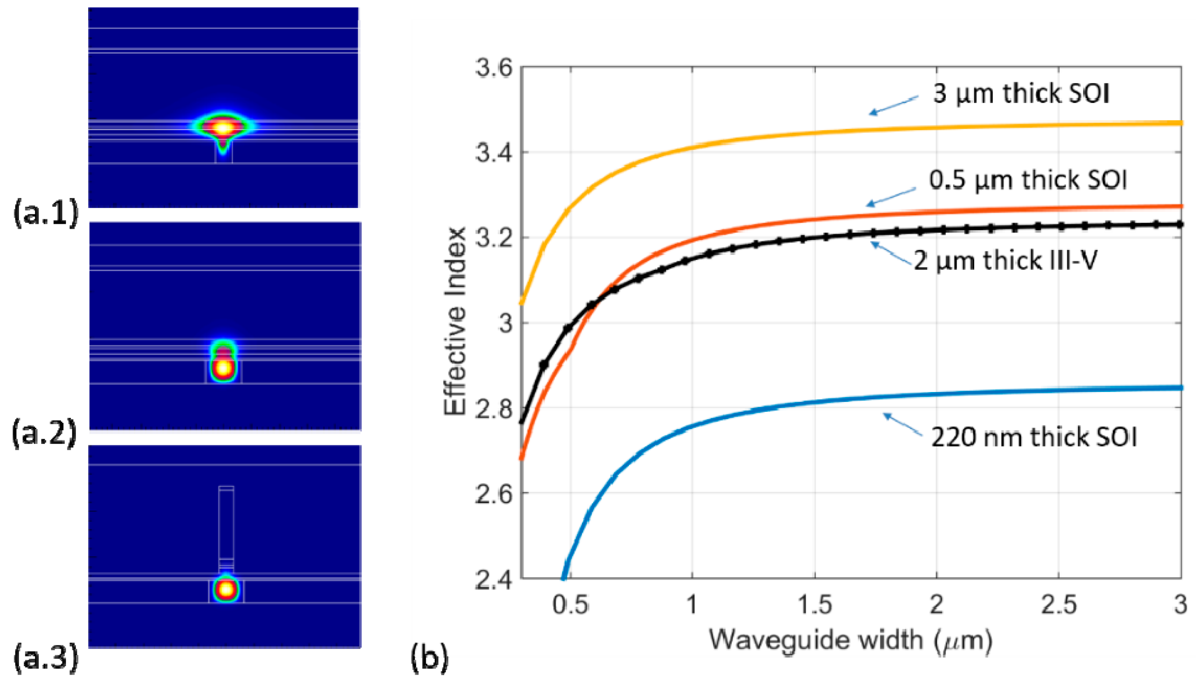
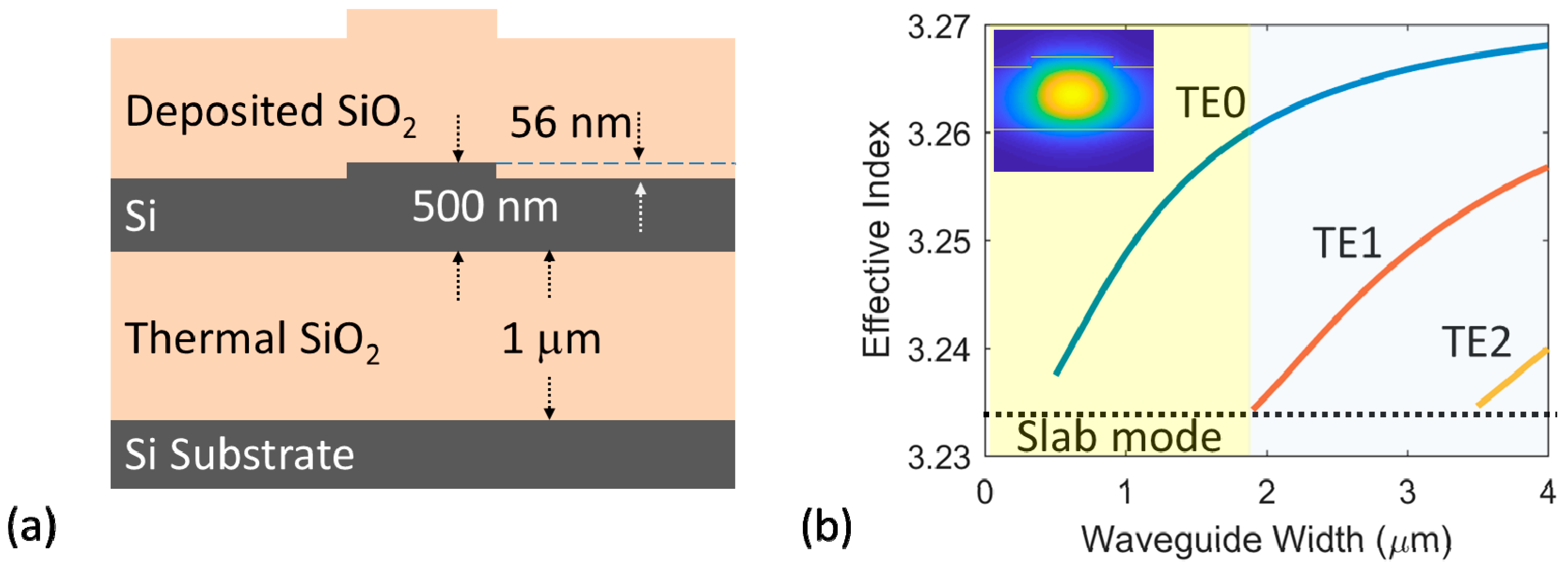
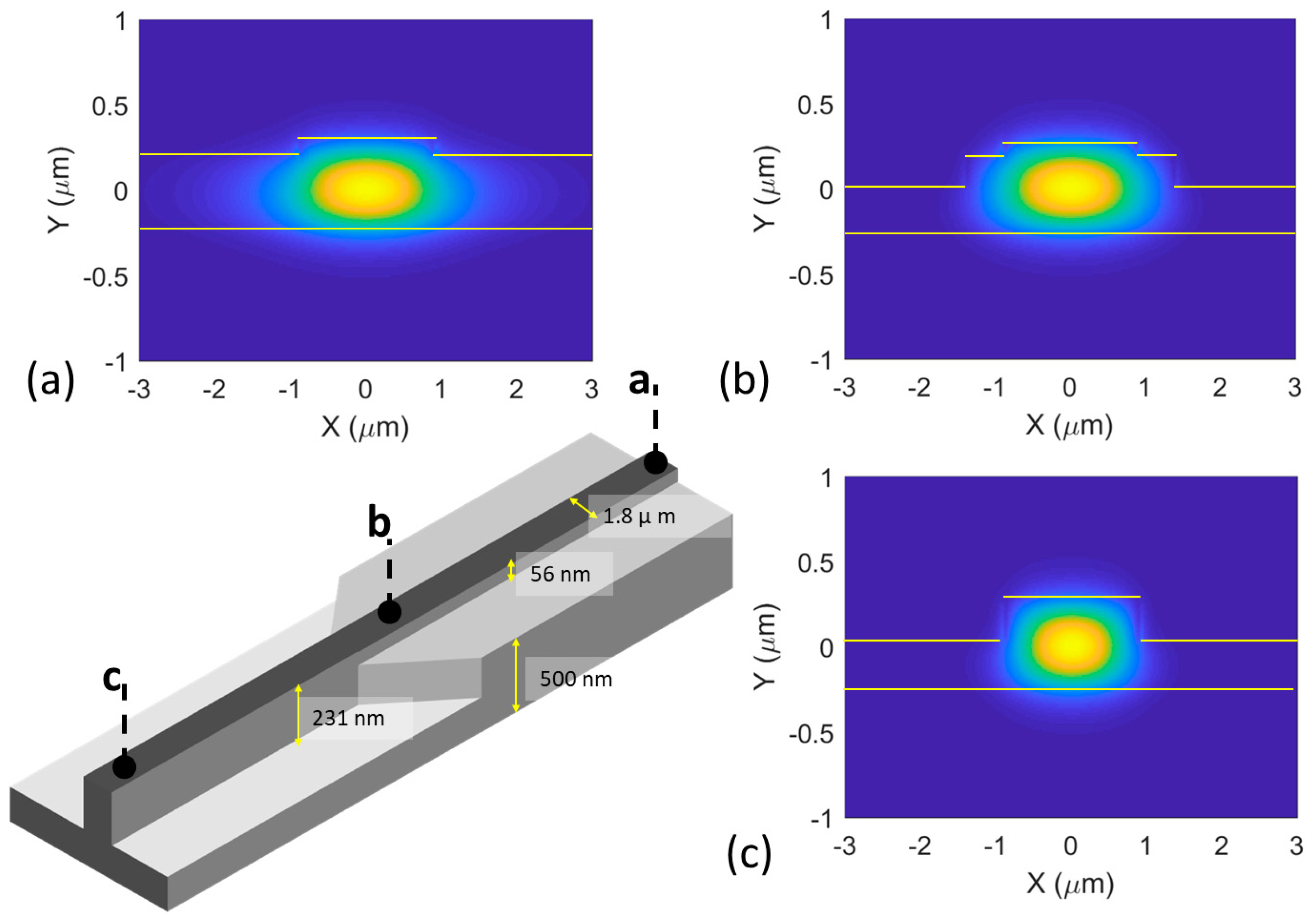
2.1. Waveguide Geometry

The ULL waveguide cross-sectional geometry is shown in Figure 2a. To lower the optical mode interaction with the rib sidewall, the waveguide rib height is targeted to be about 10% of the total Si layer thickness. An etch depth of 56 nm was chosen because it can be accurately controlled using a laser-based interferometric etch depth monitor (Intellemetrics LEP500) system, which is commercially available. Thermal oxide serves as the bottom buried oxide (BOX) while the top cladding is deposited oxide, either by plasma-enhanced chemical vapor deposition (PECVD) or sputtering. Each cladding layer is 1 µm thick to minimize substrate leakage or loss due to the metal heaters, which are commonly put on the top of the waveguide resonators. The effective index of the transverse electric (TE) modes versus the waveguide width is plotted in Figure 2b, suggesting that the waveguide guides a single TE mode when the width is 1.8 µm or lower.

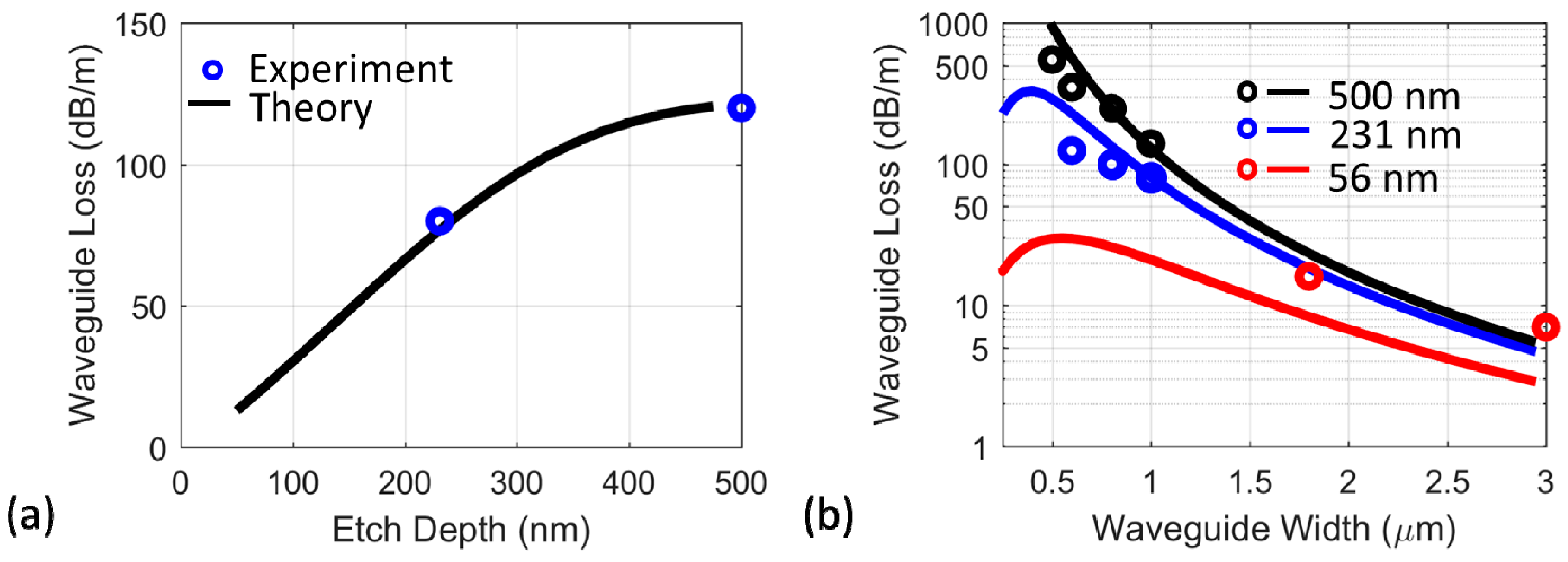
2.2. Waveguide Loss Consideration

Due to the line-edge roughness associated with optical lithography, which is further aggravated in dry-etching processes, the propagation loss of the planar waveguides is typically dominated by the radiative loss induced by the interaction between the optical mode and the roughness on the waveguide sidewalls. Here, we estimate the waveguide radiative loss using the nw model approximation [30]. This approximation is particularly useful if one only needs to quantify the relative comparisons of the propagation losses among different waveguide geometries under the same fabrication conditions. According to this model, waveguide loss can be approximated as:
α r = A ( σ , L c , n e f f ) n e f f w
where A is the proportionality factor determined by the sidewall roughness rms (σ) and the roughness correlation length ( L c ), neff is the effective index of the waveguide optical mode, and w is the width of the waveguide. A full expression of A can be found in [31]. Given a waveguide geometry that is far from mode cut-off condition, the magnitude of the factor A in general does not depend on the waveguide width.
Figure 3a shows the measured propagation loss of the two “more conventional” silicon waveguide geometries for the heterogeneous silicon platform used in previous works [10,32,33]. One is a fully 500 nm etched strip waveguide, and the other is 231 nm etched rib waveguide. The widths of both waveguides are 1 µm. Empirical values of the roughness parameters were obtained (line edge roughness rms σ ~5 nm and correlation length L c ~60 nm) and then Equation (1) is used to generate theoretical curve corresponding to the radiative losses at varying etch depth. The theoretical waveguide loss curves with varying etching depths (500 nm, 231 nm and 56 nm) are then calculated and plotted in Figure 3b, showing a reasonable agreement with experimental data for the 500 nm and 231 nm etch depths. According to these model results, low propagation loss in the range of 3–10 dB/m can be expected for the 56 nm rib silicon waveguides with larger than 1.5 µm width.

3. Passive Device Demonstrations

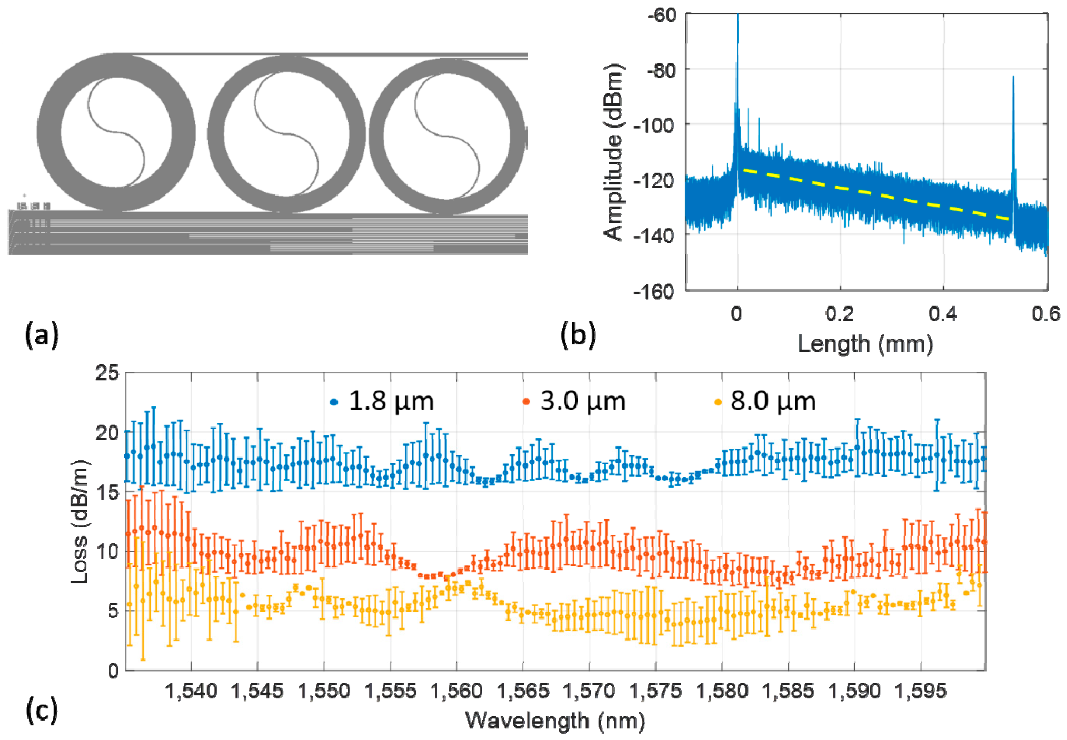
3.1. Long Waveguide Delay-Line

We designed 52.2 cm long spiral delays (illustrated in Figure 4a) to characterize the propagation loss. Waveguide widths were 1.8, 3.0 and 8.0 µm and the minimum bend radius used in all spirals was 800 µm. We use the coherent optical frequency domain reflectometry (OFDR) technique with a commercially available system (Luna Inc. OBR 4400, Roanoke, VA, USA) [34] to quantify the propagation loss of the fabricated Si rib waveguides. The technique has been proven to calculate the propagation loss with high accuracy independent of the fiber-waveguide coupling loss uncertainty [21]. Figure 4b shows the data measured for the 52.2 cm long spiral of 1.8 µm wide ULL silicon waveguide. The peaks on the left hand side (near 0 m distance) and right hand side (near 0.5 m distance) are the reflections at the waveguide facets. The linearity of the trace verifies that the waveguide loss is not bend-loss limited. The measured mean and deviation of spectral dependence of the propagation loss of the three waveguide widths are plotted in Figure 4c. A single mode 1.8 µm wide waveguide achieves an average of 16 dB/m propagation loss over C + L band. The propagation loss in multimode ULL waveguide with 3.0 µm and 8.0 µm widths are lower, at 10 dB/m and 4 dB/m, respectively.
The measured loss of the ULL waveguides show a relatively large discrepancy to the values predicted by the nw approximation method described in Section 2.2 (Figure 2b). The model had several simplifications such as ignoring the surface roughness of the etched slab surfaces. For fully etched (500 nm) or halfway etched (231 nm) waveguides, the optical field that interacts with the etched surface is small enough to be neglected in the total loss calculation. However, with the very shallow rib (56 nm) waveguides, the optical field expands laterally (similar to a slab mode) and the interaction between the mode field and the etched surface cannot be ignored. The roughness rms of the etched surface is typically in order of several nanometers, which is more than one order of magnitude larger than the unetched waveguide top surface roughness (~0.1 nm). The scattering due to the etched surface roughness is therefore significant and results in the discrepancy between the experimental and theoretical waveguide loss.

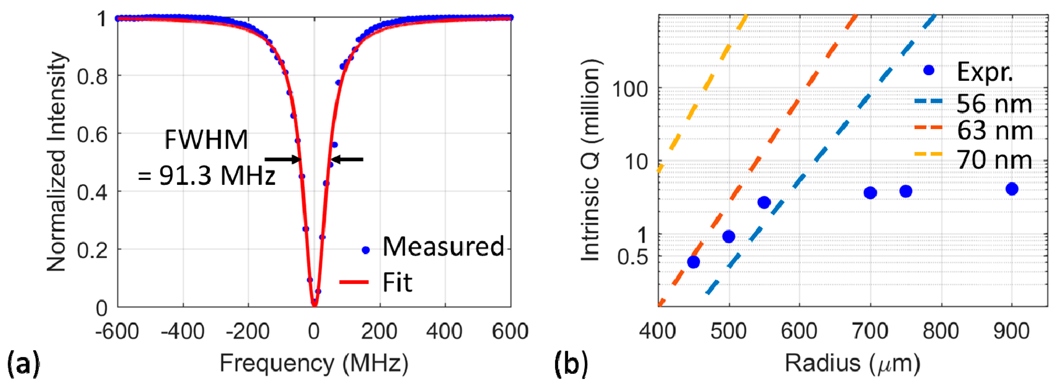
3.2. High Quality Factor Ring Resonators

One key component made possible by low-loss waveguides is the high-Q ring resonator. The ring resonator is an essential building block to realize compact optical filters and delays on chip. Higher Q-factors enable sharper, narrowband filters and longer delays, which are requirements for the aforementioned ultra-long laser cavity. There has been a plethora of recent work to demonstrate high-Q integrated resonators using different materials and cavity geometries. These results include fully integrated resonators with an intrinsic Q of 22 million in silicon [26], 81 million in a silicon nitride resonator [35] and over 200 million in a silica resonator [36]. However, the results of the latter two are multimoded, which can lead to multiple sets of resonances or excess loss at the coupling regions unless special care is taken to optimize the coupler [37]. These three results all have bend radii >2 mm, which limits the compactness of the device, and complicates the design of a Vernier-effect filter due to the small free spectral range of each ring. Finally, it is unlikely that these resonators were designed with laser integration in mind, and cannot be integrated with the heterogeneous silicon/III-V laser without significant extra processing [25,38].
In this work, we demonstrate ring resonators readily integratable with the heterogenous silicon/III-V platform with a loaded Q of 2.1 million, and an intrinsic Q of 4.1 million. The ring is in an all-pass configuration, and is 1.8 microns in width, which is single-mode for the TE polarization. The ring is connected to a bus waveguide of the same dimensions using a straight-to-curved coupler with a 1.2 micron coupling gap. The transmission spectra of the ring is measured by sweeping a high-resolution tunable laser (0.1 pm steps) across the resonance, and measuring the output power. The resulting spectra is depicted in Figure 5a, and fitted with a Lorentzian function. The measured full width half max (FWHM) is 91.3 MHz.
The ring in Figure 5a has a 750 µm bend radius, for which we did not observe any bend-loss induced radiation in the resonator. To confirm this, we investigated rings with varying radii, and plot their intrinsic Q factor alongside the theoretical bend-loss limit for Q in Figure 5b. The experimental results are extracted from the measured FWHM, while the dashed lines are simulated using Lumerical MODE solutions. The simulations are shown for three different etch depths, as that is the most sensitive parameter to the bend-loss. We find that our ring in this experiment is actually overetched compared to the target 56 nm, judging by the Q of the smaller rings. We do not observe significant bend loss in the rings until the radius is less than 550 µm. For practical reasons, the ring radius should be larger than 700 µm to avoid bend-loss possibly caused by an underetch of the waveguide.

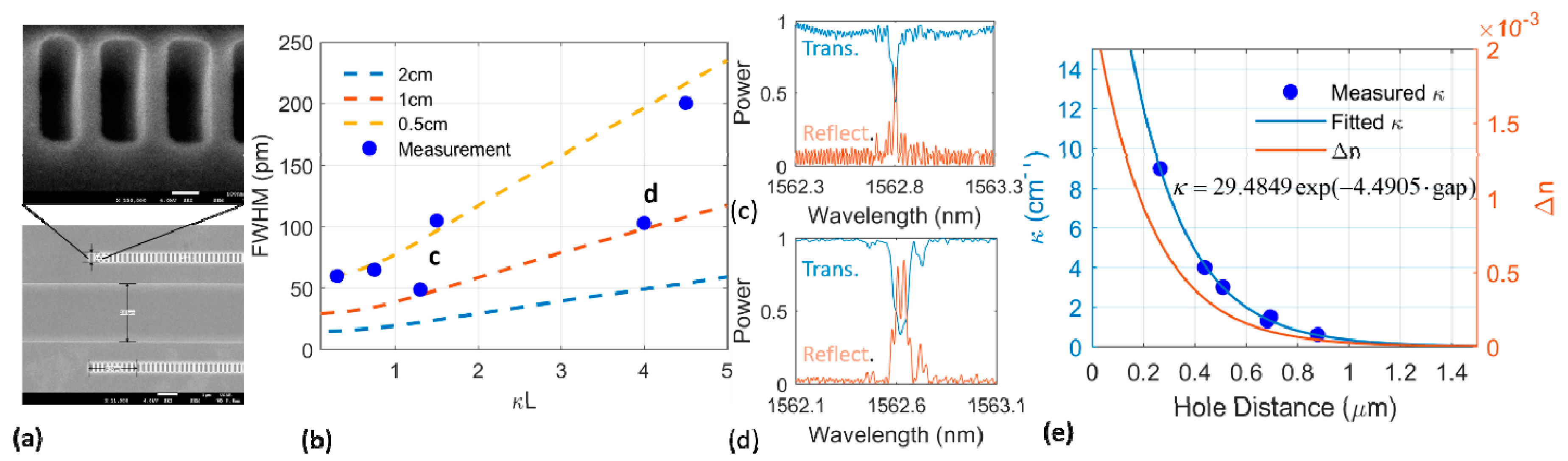
3.3. Narrow Bandwidth Bragg Gratings

Another useful component that can be utilized with low-loss waveguides is a low-kappa (κ) Bragg grating. These gratings are widely used in filters, sensors, and semiconductor lasers as a wavelength selective element, much like the ring resonator. The bandwidth of the grating is directly proportional to power coupling coefficient κ, and therefore can be minimized by reducing the perturbation strength of the grating [39]. At the same time, the length (L) of the grating should be long enough (κL ~ 1) and the loss of the waveguide must be low in order to obtain sufficient reflection. Care must be taken in the design of the grating in order to achieve weak κ as conventional sidewall or top surface gratings tend to have stronger κ. Instead, we utilize “post” (or inversely, “hole”) gratings in which small areas of the waveguiding material are placed (removed) periodically on either side of the waveguide. The dimensions of the posts (holes) and proximity to the waveguide can be lithographically defined, and tailored to achieve the desired κ. This approach has been successful for low loss silicon nitride gratings [40]. For our waveguides, it is simpler to etch holes on either side of the waveguide, as shown in Figure 6a. The resulting κ of the grating is directly controlled by the hole-to-waveguide distance, while the period of the grating is set to be 240 nm, corresponding to a stopband at 1563 nm for an unperturbed waveguide neff = 3.2560.
We fabricate uniform gratings with lengths of 0.5 and 1.0 cm. The waveguide width is 1.8 µm, and the length is 2.2 cm. We used an e-beam lithography to write the grating teeth, although DUV immersion lithography can also resolve 120 nm features. Transmission and reflection spectra are measured, and fitted using a transfer matrix model in Lumerical Interconnect. This approach also accounts for Fabry-Perot cavities formed by the waveguide facets, which affects the grating shape. From this, we extract the bandwidth and peak reflectivity of the grating, which can then be used to estimate κ. A few selected gratings are depicted in Figure 6b along with the predicted grating bandwidth. Using 1 cm long gratings, we were able to achieve a 50 pm FWHM bandwidth with roughly 70% reflectivity, with potential to further reduce the bandwidth with a longer grating. Figure 6c and d show two examples of the measured reflection and transmission spectra of the 1 cm long grating waveguides with κ = 1.25 cm−1 and κ = 4.0 cm−1, respectively. Finally, Figure 6e shows the relation between the distance between the holes to the core waveguide’s edge and κ strength. The measured data was fitted well with an exponential curve. The right y-axis of Figure 6e shows the calculated effective index difference between the waveguide with and without the hole gratings.

4. Photonic Integrated Circuits with Ultralow Loss Silicon Waveguides

The ability to integrate ultralow loss waveguides inside the laser cavity or form fully integrated delay lines with active devices promises vastly superior performance at much-reduced footprint compared to e.g., fiber-based delays. Furthermore, full integration improves the robustness of devices and reduces cost of packaging. The key for integration is a low loss taper to transition from ULL waveguides to a waveguide geometry with smaller bend radius, which we describe in detail in following section. This allows us to expand the versatility of the heterogeneous silicon platform. Finally, we give two applications that benefit greatly from having ULL waveguides: narrow linewidth lasers and interferometric optical gyroscopes.

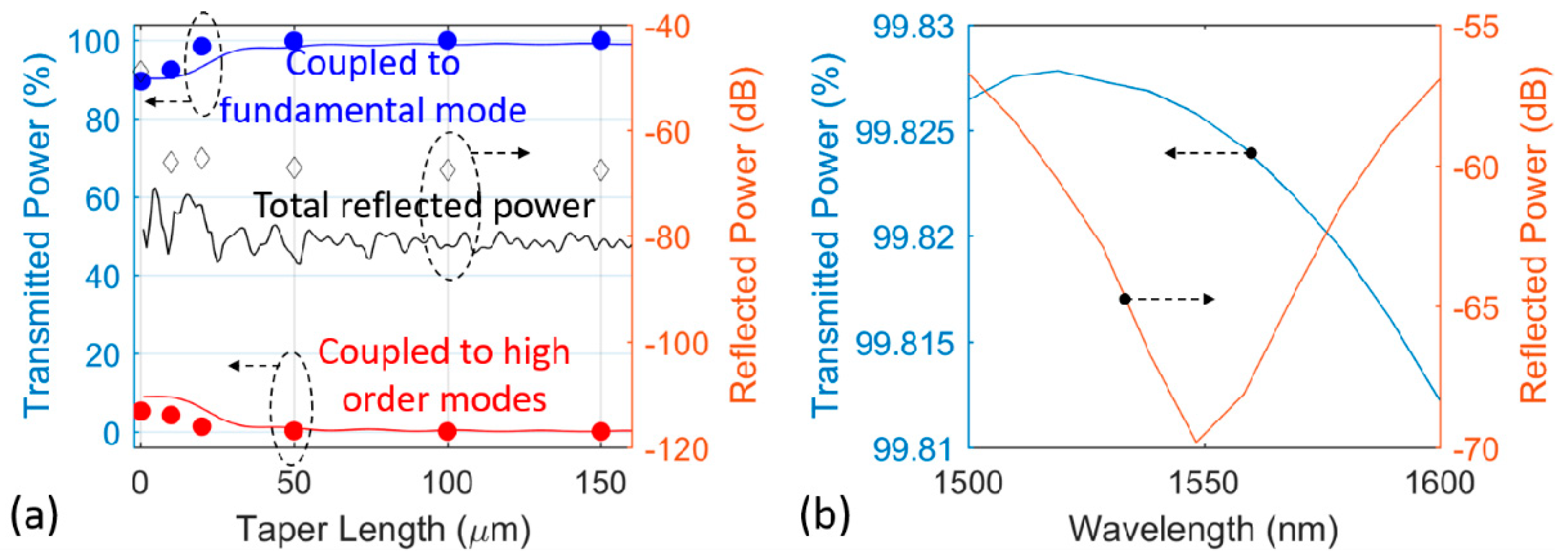
4.1. Transition Taper to Standard Silicon Waveguides

Figure 7 shows the schematic of an adiabatic taper for a low loss, low reflection transition of the optical mode from the 56 nm etched rib ULL waveguide to a deeper 231 nm etched rib waveguide, which has a smaller bend radius (50 µm). The waveguide width is set at 1.8 µm. The mode transition happens along the linear taper formed by etching on the Si slab. Figure 7a–c shows the simulated profiles of the waveguide’s fundamental mode at points a, b and c denoted on the schematic figure.
In order to ensure an adiabatic transition from fundamental mode of the 56 nm etched waveguide to the 231 nm etched waveguide, the length of the linear taper must be sufficiently long. As shown in Figure 8a, at 1550 nm wavelength, high order modes in the deeper rib waveguide are excited if the taper length is shorter than 25 µm. With a taper longer than 50 µm, both mode expansion and finite-difference time-domain (FDTD) simulations show that essenstially 100% transmission in the fundamental mode is achieved. The reflection power is also simulated and is shown to be lower than −60 dB level. To be safe, the taper length of 200 µm is chosen in practice. The wavelength dependence of the transmission efficiency and reflection power are again simulated in FDTD and shown in Figure 8b. Larger than 99.8% transmission and lower than −55 dB reflection should be achievable over the whole C + L band.

4.2. Applications

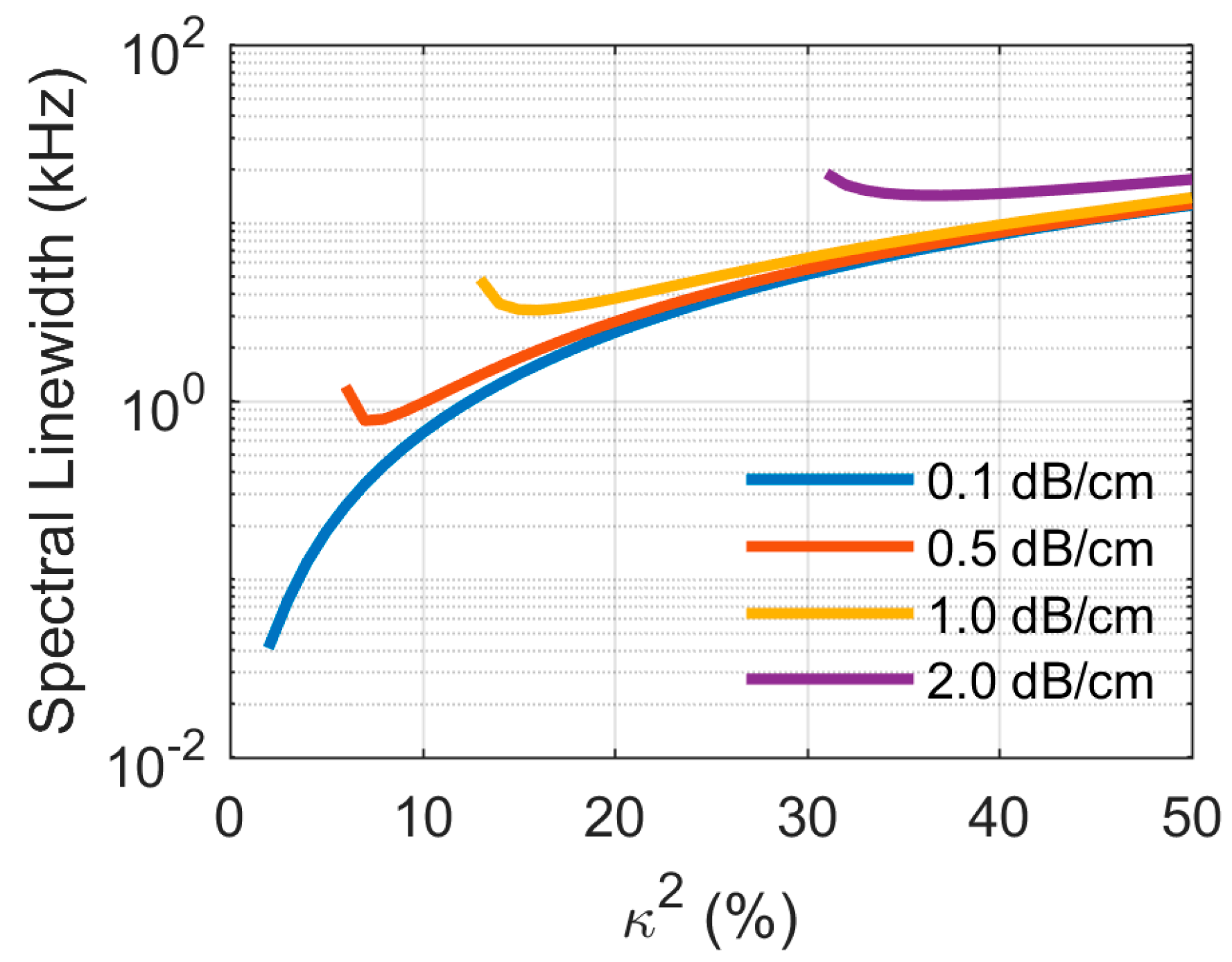
4.2.1. Extended Cavity Lasers

The heterogeneous silicon platform has demonstrated superior laser linewidth performance compared to typical linewidths of III/V lasers that are in a few MHz range [41]. There are at least two reasons for superior linewidth. The platform allows for the control of confinement in the quantum wells and provides a low-loss waveguide platform, opening a new possibility in improving the coherence by providing a mechanism to separate the photon resonator (in silicon) and highly-absorbing active medium [42]. The second improvement comes with to the use of ring resonators inside the laser cavity to create a widely-tunable laser. Ring resonators, provided that the utilized waveguide platform offers sufficiently low propagation losses, have an advantage as the effective cavity length at ring resonance is significantly enhanced, directly reducing linewidth. Both reasons benefit from loss reduction, and it was predicted that sub-kHz Lorentzian linewidths should be attainable with waveguide platform providing sub-0.5 dB/cm propagation loss [43].
We extend the analysis to platform providing 0.1 dB/cm propagation and keep the same basic laser structure as in [43] comprising of three ring resonators inside the Fabry-Perot laser cavity. The estimated Lorentzian linewidth for optimized laser fabricated with such low-loss waveguides is sub-100 Hz as shown in Figure 9.

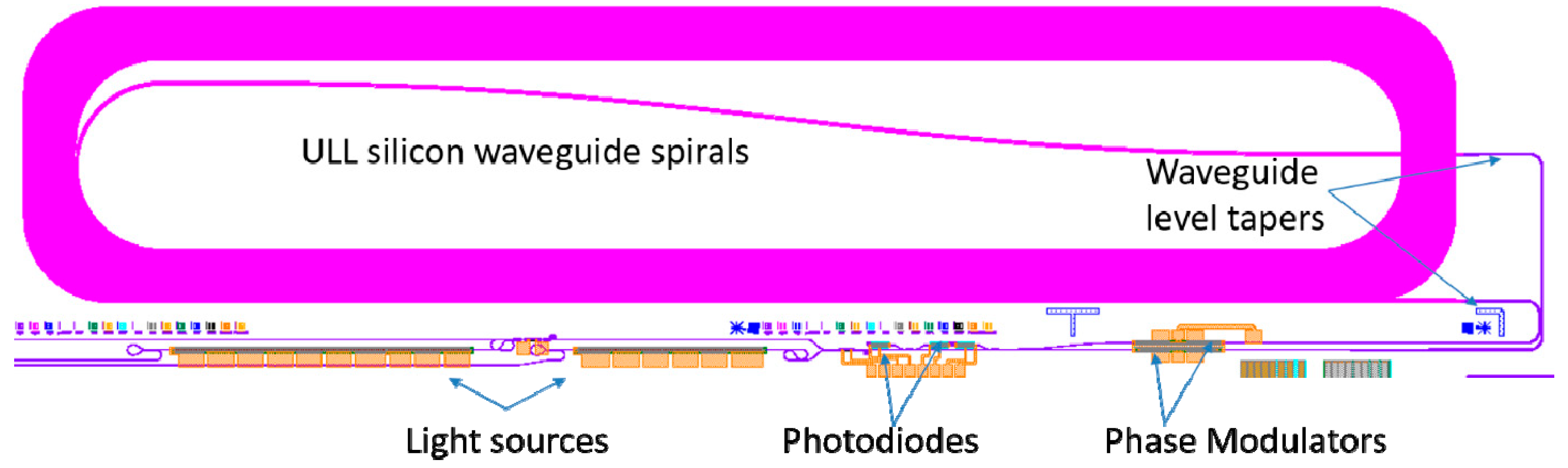
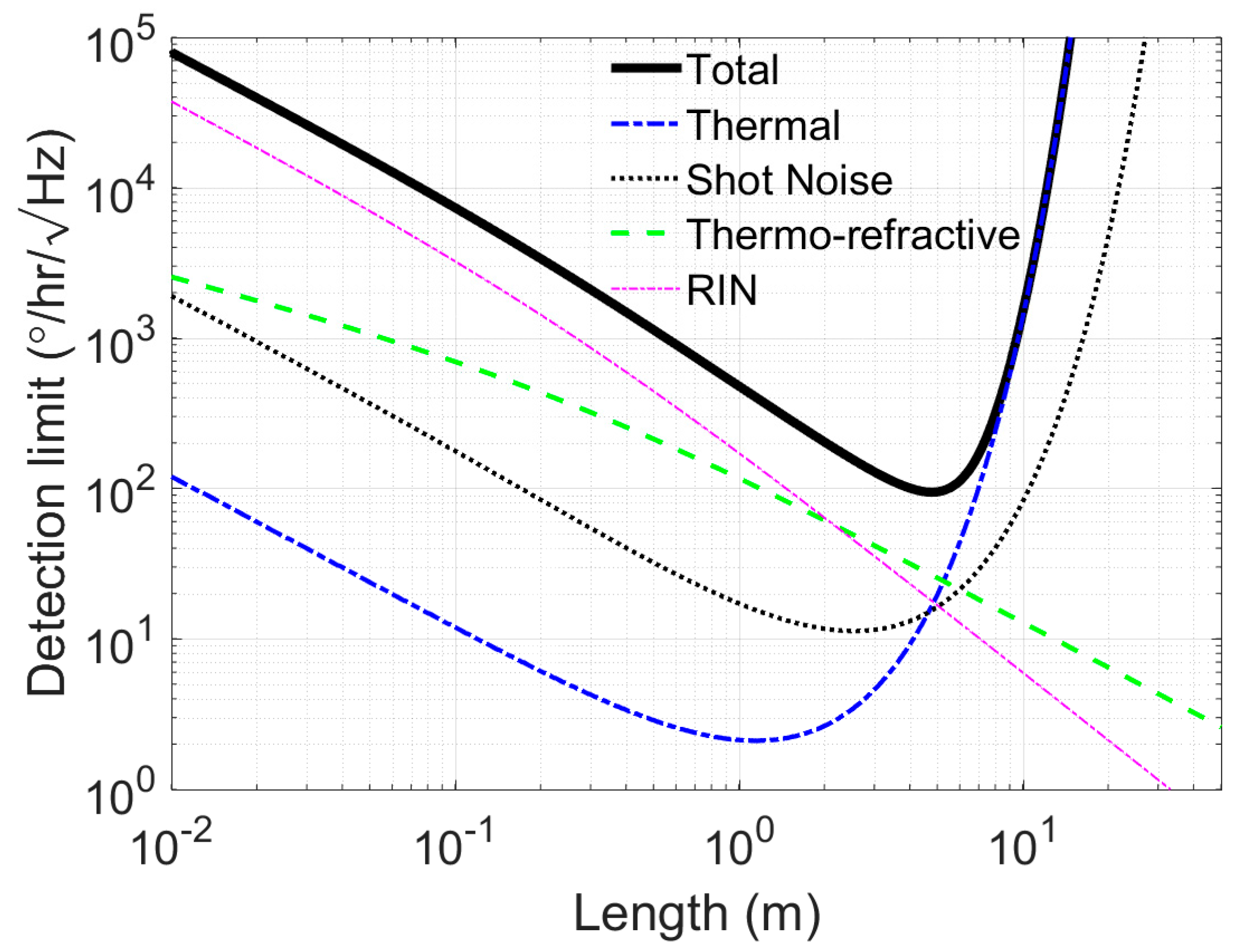
4.2.2. Optical Gyroscopes

Low SWAP and low cost gyroscopes are of great improtance in the fields of robotics, unmanned aerial vehicle and automotives and recently has rapidly become even more so with the emergence of augmented reality technology and drones. In many applications that operate in environments with high shock and vibrations, optical gyroscopes are more robust and reliable compared to their MEMS counterparts because they do not have any moving parts. However, the large size and cost of traditional optical gyroscopes, which are based on discrete components, make them difficult to be as widely usable as MEMS gyros. In a previous work [10], we used integrated silicon photonics to miniaturize the optical driver (OD) part for interferometric fiber gyroscopes (IFOGs) to a small chip. The integrated OD chip contains every optical component needed for the gyroscope, except the fiber sensing coil, which needs to be sufficiently long to achieve high sensitivity. For applications that require lower sensivity, however, an integrated waveguide-based delayline might deliver adequate performance. In the following, we show the architecture of an interferometric optical gyroscope fully integrated on silicon, making use of the ULL Si waveguide as its Sagnac sensing coil.
The schematic mask layout of the integrated gyroscope is shown in Figure 10. The general architecture of the circuit is very similar to [44]: The light from the sources goes through two 3-dB broadband couplers to get splitted into two waves and then goes through push-pull phase modulators. The two waves enter the ULL silicon waveguide sensing coil (with 4 dB/m propagation loss) and propagate in counter-directions before coming back to beat on a photodiode on a port of the first 3-dB coupler. The Sagnac phase shift can be detected and used to measure the rotation of the system.
The sensitivity of the proposed gyroscope as a function of the length of the Sagnac waveguide coil is estimated by taking into account four sources of noise, i.e., thermal noise, shot noise, relative intensity noise and thermo-refractive noise. The anaslysis is performed in the same manner in our previous work [44] and the contribution from each noise term to rotation nosie spectral density are depicted in Figure 11. A 50 mW output power from the light sources, 4 dB/m loss in the ULL silicon waveguide coil, and 0.02 dB/crossing (simulated value) were assumed. The minimum detection limit of the gyroscope is approximated to be 113 ° / h r / H z or equivalently 1.88 ° / h r .

5. Conclusions

In conclusion, we have demonstrated ULL silicon waveguides using 500 nm thick SOI that can be seamlessly integrated with heterogeneous silicon/III-V active components such as lasers, modulators, and photodetectors. Waveguide loss is as low as 4 dB/m for a multimode waveguide, and 16 dB/m for a quasi-single mode waveguide. The ultralow loss directly benefits applications such as optical gyroscopes in which a long delay line is needed. It can also be utilized in high-Q ring resonators and narrowband grating-based filters. We demonstrate rings with 4.1 million intrinsic Q, which are promising to realize narrow linewidth lasers on silicon. Calculations show that linewidths on the order of 100 Hz should be achievable using these waveguides.

Author Contributions

M.A.T. designed the devices; M.A.T., D.H. performed the experiments; M.A.T., D.H., T.K. simulated and analyzed the data; J.P., D.H., A.M. fabricated the devices; M.A.T., D.H., T.K., J.E.B. wrote the manuscript; J.E.B. supervised the project.

Funding

DARPA MTO Contract N66001-16-C-4017.

Acknowledgments

This work was supported by DARPA MTO. The views and conclusions contained in this document are those of the authors and should not be interpreted as representing official policies of DARPA or the U.S. Government. The authors would like to thank Paolo Pintus for help with simulation, Michael Davenport for processing advice, Andreas Boes for help with testing, Warren Jin, Chao Xiang and Paul Morton for fruitful discussions.

Conflicts of Interest

The authors declare no conflict of interest.

References

  1. Coldren, L.A.; Corzine, S.W.; Masanovic, M.L. Diode Lasers and Photonic Integrated Circuits, 2nd ed.; Wiley: Hoboken, NJ, USA, 2012. [Google Scholar]
  2. Okamoto, K. Progress and technical challenge for planar waveguide devices: Silica and silicon waveguides. Laser Photonics Rev. 2012, 6, 14–23. [Google Scholar] [CrossRef]
  3. Bauters, J.F.; Heck, M.J.R.; Demis, J.; Dai, D.; Tien, M.; Barton, J.S.; Leinse, A.; Heideman, R.G.; Blumenthal, D.J.; Bowers, J.E. Ultra-low-loss high-aspect-ratio Si3N4 waveguides. Opt. Express 2011, 19, 3163–3174. [Google Scholar] [CrossRef] [PubMed]
  4. Thomson, D.; Zilkie, A.; Bowers, J.E.; Komljenovic, T.; Reed, G.T.; Vivien, L.; Marris-Morini, D.; Cassan, E.; Virot, L.; Fédéli, J.M.; et al. Roadmap on silicon photonics. J. Opt. (United Kingdom) 2016, 18, 073003. [Google Scholar] [CrossRef] [Green Version]
  5. Roelkens, G.; Abassi, A.; Cardile, P.; Dave, U.; de Groote, A.; de Koninck, Y.; Dhoore, S.; Fu, X.; Gassenq, A.; Hattasan, N.; et al. III-V-on-Silicon Photonic Devices for Optical Communication and Sensing. Photonics 2015, 2, 969–1004. [Google Scholar] [CrossRef] [Green Version]
  6. Aalto, T.; Harjanne, M.; Cherchi, M. VTT’s micron-scale silicon rib+strip waveguide platform. Int. Soc. Opt. Photonics 2016, 9891, 98911G. [Google Scholar] [CrossRef]
  7. Komljenovic, T.; Davenport, M.; Hulme, J.; Liu, A.Y.; Santis, C.T.; Spott, A.; Srinivasan, S.; Stanton, E.J.; Zhang, C.; Bowers, J.E. Heterogeneous silicon photonic integrated circuits. J. Light. Technol. 2016, 34, 20–35. [Google Scholar] [CrossRef]
  8. Zhang, C.; Zhang, S.; Peters, J.D.; Bowers, J. E. 8 × 8 × 40 Gbps fully integrated silicon photonic network on chip. Optica 2016, 3, 785–786. [Google Scholar] [CrossRef]
  9. Hulme, J.; Kennedy, M.; Chao, R.-L.; Liang, L.; Komljenovic, T.; Shi, J.-W.; Szafraniec, B.; Baney, D.; Bowers, J.E. Fully integrated microwave frequency synthesizer on heterogeneous silicon-III/V. Opt. Express 2017, 25, 2422–2431. [Google Scholar] [CrossRef] [PubMed]
  10. Tran, M.A.; Komljenovic, T.; Hulme, J.C.; Kennedy, M.; Blumenthal, D.J.; Bowers, J.E. Integrated optical driver for interferometric optical gyroscopes. Opt. Express 2017, 4, 3826–3840. [Google Scholar] [CrossRef] [PubMed]
  11. Hulme, J.C.; Doylend, J.K.; Heck, M.J.R.; Peters, J.D.; Davenport, M.L.; Bovington, J.T.; Coldren, L.A.; Bowers, J.E. Fully integrated hybrid silicon two dimensional beam scanner. Opt. Express 2015, 23, 5861–5874. [Google Scholar] [CrossRef] [PubMed]
  12. Pavesi, L.; Editors, D.J.L. Topics in Applied Physics 122 Silicon Photonics III Systems and Applications. In Silicon Photonics III; Springer: Berlin/Heidelberg, Germany, 2016. [Google Scholar]
  13. Xu, D.-X.; Schmid, J.; Reed, G.; Mashanovich, G.; Thomson, D.; Nedeljkovic, M.; Chen, X.; Van Thourhout, D.; Keyvaninia, S.; Selvaraja, S. Silicon photonic integration platform–Have we found the sweet spot? IEEE J. Sel. Top. Quantum Electron. 2014, 20, 189–205. [Google Scholar]
  14. Ferrotti, T.; Blampey, B.; Jany, C.; Duprez, H.; Chantre, A.; Boeuf, F.; Seassal, C.; Ben Bakir, B. Co-integrated 13 µm hybrid III-V/silicon tunable laser and silicon Mach-Zehnder modulator operating at 25Gb/s. Opt. Express 2016, 24, 30379–30401. [Google Scholar] [CrossRef] [PubMed]
  15. Selvaraja, S.K.; De Heyn, P.; Winroth, G.; Ong, P.; Lepage, G.; Cailler, C.; Rigny, A.; Bourdelle, K.; Bogaerts, W.; VanThourhout, D.; et al. Highly uniform and low-loss passive silicon photonics devices using a 300 mm CMOS platform. In Proceedings of the Optical Fiber Communication Conference, OSA, Washington, DC, USA, 9–13 March 2014. [Google Scholar]
  16. Kobayashi, N.; Sato, K.; Namiwaka, M.; Yamamoto, K.; Watanabe, S.; Kita, T.; Yamada, H.; Yamazaki, H. Silicon photonic hybrid ring-filter external cavity wavelength tunable lasers. J. Light. Technol. 2015, 33, 1241–1246. [Google Scholar] [CrossRef]
  17. Gao, F.; Wang, Y.; Cao, G.; Jia, X.; Zhang, F. Improvement of sidewall surface roughness in silicon-on-insulator rib waveguides. Appl. Phys. B Lasers Opt. 2005, 81, 691–694. [Google Scholar] [CrossRef]
  18. Kurczveil, G.; Heck, M.J.R.; Garcia, J.M.; Poulsen, H.N.; Park, H.; Blumenthal, D.J.; Bowers, J.E. Integrated recirculating optical hybrid silicon buffers. In Proceedings of the Silicon Photonics VI, San Francisco, CA, USA, 17 January 2011; Kubby, J.A., Reed, G.T., Eds.; p. 79430U. [Google Scholar] [CrossRef]
  19. Gundavarapu, S.; Belt, M.; Huffman, T.A.; Tran, M.A.; Komljenovic, T.; Bowers, J.E.; Blumenthal, D.J. Interferometric Optical Gyroscope Based on an Integrated Si3N4 Low-Loss Waveguide Coil. J. Light. Technol. 2018, 36, 1185–1191. [Google Scholar] [CrossRef]
  20. Cherchi, M.; Ylinen, S.; Harjanne, M.; Kapulainen, M.; Vehmas, T.; Aalto, T. Low-loss spiral waveguides with ultra-small footprint on a micron scale SOI platform. In Proceedings of the Conference on Silicon Photonics IX, San Francisco, CA, USA, 3–5 February 2014. [Google Scholar]
  21. Bauters, J.F.; Heck, M.J.R.; John, D.D.; Barton, J.S.; Bruinink, C.M.; Leinse, A.; Heideman, R.G.; Blumenthal, D.J.; Bowers, J.E. Planar waveguides with less than 0.1 dB/m propagation loss fabricated with wafer bonding. Opt. Express 2011, 19, 24090–24101. [Google Scholar] [CrossRef] [PubMed]
  22. Pfeiffer, M.H.P.; Kordts, A.; Brasch, V.; Zervas, M.; Geiselmann, M.; Jost, J.D.; Kippenberg, T.J. Photonic Damascene process for integrated high-Q microresonator based nonlinear photonics. Optica 2016, 3, 20–25. [Google Scholar] [CrossRef]
  23. Ji, X.; Barbosa, F.A.S.; Roberts, S.P.; Dutt, A.; Cardenas, J.; Okawachi, Y.; Bryant, A.; Gaeta, A.L.; Lipson, M. Ultra-low-loss on-chip resonators with sub-milliwatt parametric oscillation threshold. Optica 2017, 4, 619–624. [Google Scholar] [CrossRef]
  24. Lee, H.; Chen, T.; Li, J.; Yang, K.Y.; Jeon, S.; Painter, O.; Vahala, K.J. Chemically etched ultrahigh-Q wedge-resonator on a silicon chip. Nat. Photonics 2012, 6, 369–373. [Google Scholar] [CrossRef]
  25. Davenport, M.; Bauters, J.; Piels, M.; Chen, A.; Fang, A.; Bowers, J.E. A 400 Gb/s WDM Receiver Using a Low Loss Silicon Nitride AWG Integrated with Hybrid Silicon Photodetectors. In Proceedings of the Conference on Optical Fiber Communication (OFC)/National Fiber Optic Engineers Conference (NFOEC), Anaheim, CA, USA, 17–21 March 2013. [Google Scholar]
  26. Biberman, A.; Shaw, M.J.; Timurdogan, E.; Wright, J.B.; Watts, M.R. Ultralow-loss silicon ring resonators. Opt. Lett. 2012, 37, 4236–4238. [Google Scholar] [CrossRef] [PubMed]
  27. Yariv, A.; Sun, X. Supermode Si/III-V hybrid lasers, optical amplifiers and modulators: A proposal and analysis. Opt. Express 2007, 15, 9147–9151. [Google Scholar] [CrossRef] [PubMed]
  28. Sun, X.; Yariv, A. Engineering supermode silicon/III-V hybrid waveguides for laser oscillation. J. Opt. Soc. Am. B 2008, 25, 923–926. [Google Scholar] [CrossRef] [Green Version]
  29. Davenport, M.L.; Skendzic, S.; Volet, N.; Hulme, J.C.; Heck, M.J.R.; Bowers, J.E. Heterogeneous silicon/III–V semiconductor optical amplifiers. IEEE J. Sel. Top. Quantum Electron. 2016, 22, 78–88. [Google Scholar] [CrossRef]
  30. Melati, D.; Melloni, A.; Morichetti, F. Real photonic waveguides: Guiding light through imperfections. Adv. Opt. Photonics 2014, 6, 156–224. [Google Scholar] [CrossRef]
  31. Melati, D.; Morichetti, F.; Melloni, A. A unified approach for radiative losses and backscattering in optical waveguides. J. Opt. 2014, 16, 055502. [Google Scholar] [CrossRef]
  32. Davenport, M.L.; Liu, S.; Bowers, J.E. Integrated heterogeneous silicon/III–V mode-locked lasers. Photonics Res. 2018, 6, 468–478. [Google Scholar] [CrossRef]
  33. Tran, M.A.; Zhang, C.; Bowers, J.E. A broadband optical switch based on adiabatic couplers. In Proceedings of the 29th IEEE Photonics Conference (IPC), Waikoloa, HI, USA, 2–6 October 2016. [Google Scholar]
  34. Soller, B.J.; Gifford, D.K.; Wolfe, M.S.; Froggatt, M.E. High resolution optical frequency domain reflectometry for characterization of components and assemblies. Opt. Express 2005, 13, 666–674. [Google Scholar] [CrossRef] [PubMed]
  35. Spencer, D.T.; Tang, Y.; Bauters, J.F.; Heck, M.J.R.; Bowers, J.E. Integrated Si3N4/SiO2 ultra high Q ring resonators. Optica 2012, 4, 141–142. [Google Scholar]
  36. Yang, K.Y.; Oh, D.Y.; Lee, S.H.; Yang, Q.-F.; Yi, X.; Shen, B.; Wang, H.; Vahala, K. Bridging ultrahigh-Q devices and photonic circuits. Nat. Photonics 2018, 12, 297–302. [Google Scholar] [CrossRef]
  37. Pfeiffer, M.H.P.; Liu, J.; Geiselmann, M.; Kippenberg, T.J. Coupling ideality of integrated planar high-Q microresonators. Phys. Rev. Appl. 2017, 7, 024026. [Google Scholar] [CrossRef]
  38. Davenport, M.L.; Bowers, J.E. Efficient and broad band coupling between silicon and ultra-low-loss silicon nitride waveguides. In Proceedings of the 29th IEEE Photonics Conference (IPC), Waikoloa, HI, USA, 2–6 October 2016. [Google Scholar]
  39. Poulin, M.; Painchaud, Y.; Aubé, M.; Ayotte, S.; Latrasse, C.; Brochu, G.; Pelletier, F.; Morin, M.; Guy, M.; Cliche, J.-F. Ultra-narrowband fiber Bragg gratings for laser linewidth reduction and RF filtering. In Proceedings of the Conference on Laser Resonators and Beam Control XII, San Francisco, CA, USA, 24–27 January 2010. [Google Scholar]
  40. Spencer, D.T.; Davenport, M.; Srinivasan, S.; Khurgin, J.; Morton, P.A.; Bowers, J.E. Low kappa, narrow bandwidth Si3N4 Bragg gratings. Opt. Express 2015, 23, 30329–30336. [Google Scholar] [CrossRef] [PubMed]
  41. Komljenovic, T.; Liang, L.; Chao, R.-L.; Hulme, J.; Srinivasan, S.; Davenport, M.; Bowers, J.E. Widely-tunable ring-resonator semiconductor lasers. Appl. Sci. 2017, 7, 732. [Google Scholar] [CrossRef]
  42. Santis, C.T.; Steger, S.T.; Vilenchik, Y.; Vasilyev, A.; Yariv, A. High-coherence semiconductor lasers based on integral high-Q resonators in hybrid Si/III-V platforms. Proc. Natl. Acad. Sci. USA 2014, 111, 2879–2884. [Google Scholar] [CrossRef] [PubMed]
  43. Komljenovic, T.; Bowers, J.E. Monolithically integrated high-Q rings for narrow linewidth widely tunable lasers. IEEE J. Quantum Electron. 2015, 51, 1–10. [Google Scholar] [CrossRef]
  44. Srinivasan, S.; Moreira, R.; Blumenthal, D.; Bowers, J.E. Design of integrated hybrid silicon waveguide optical gyroscope. Opt. Express 2014, 22, 24988–24993. [Google Scholar] [CrossRef] [PubMed]
Figure 1. (a) Optical mode profiles of the heterogeneous (Si/III-V) waveguide with 500 nm thick silicon in 3 different operating regimes: (a.1) n m v > n s i with a slab III-V on 0.7 µm wide silicon waveguide, which results in higher confinement in the active III-V layer. (a.2) n m v n s i with a slab III-V on 1.3 µm wide silicon waveguide, which results in equal confinement in the III-V and silicon. (a.3) n m v < n s i with 0.5 µm wide III-V on 1.3 µm wide silicon waveguide, which results in higher confinement in silicon. (b) Effective indices of strip silicon waveguides of three thicknesses (220 nm, 500 nm and 3 µm) with varying width is plotted together with the effective index of a typical 2 µm thick III-V waveguide (used in [29]). Noted that all simulations were carried out at 1550 nm wavelength.
Applsci 08 01139 g001
Figure 2. (a) Cross-sectional geometry of the ultra-low loss (ULL) Si waveguides in this work. The thickness of the buried oxide (BOX) and the Si device layer are 1 μm and 500 nm, respectively. The 56 nm tall Si rib is formed by dry-etching, leaving a 444 nm thick Si slab. (b) Effective index versus waveguide width in the 56 nm rib Si waveguide. The waveguide is quasi-single mode within the yellow colored region. Inset: Electric field profile of the fundamental mode in 1.8 µm wide waveguide.
Applsci 08 01139 g002
Figure 3. (a) Experimental data (circular markers) and theoretical curve (solid line) for the propagation loss of 1 µm wide waveguide at varying etch depth. (b) Theoretical calculations (solid lines) of the waveguide loss at varying waveguide width at three different etch depth (500 nm, 231 nm and 56 nm). The experimentally measured results are plotted in circular markers.
Applsci 08 01139 g003
Figure 4. (a) Mask layout of spiral delay lines with 52.2 cm total length and 850 µm minimum bend radius (b) Optical Backscatter Reflectometry (OBR) data from the spiral with 1.8 µm width. A linear fit of the waveguide backscatter is shown with the dashed red line. The propagation loss of the waveguide can be approximated as 1/2 of the slope of the fitted line. (c) Wavelength dependence of the propagation loss (mean and standard deviation) of waveguides with different widths (1.8 µm, 3.0 µm and 8.0 µm).
Applsci 08 01139 g004
Figure 5. (a) Measured spectral responses of the 750 µm radius Si ring resonator (all-pass configuration) plotted with a Lorentzian fit. The extracted intrinsic quality factor Qint = 4.1 million. (b) Simulated bend-loss limited intrinsic Q of the rings versus ring radius at three etch depths. The experimental data of the targeted 56 nm etch depth are depicted as blue circular markers.
Applsci 08 01139 g005
Figure 6. (a) An SEM image of the fabricated low κ Bragg grating waveguide with a close-up of the holes on both sides of the waveguide. (b) Theoretical calculations of gratings’ full width half max (FWHM) versus varying κL for 0.5, 1 and 2 cm long grating waveguides. Circular blue markers show the measured data. (c,d) Spectra of reflection and transmission of 1 cm long grating waveguides with κ = 1.25 cm−1 and κ = 4.0 cm−1, respectively. The ripples are caused by reflections off the waveguide facets. (e) The extracted κ, Δn, and exponential fit as a function of waveguide to hole distance.
Applsci 08 01139 g006
Figure 7. Schematic of the taper converting the optical mode from an ULL waveguide to standard rib (231 nm etch depth) waveguide. Figures (ac) show the waveguide mode profiles at locations labeled a—ULL silicon waveguide, b—central part of the taper, and c—standard silicon waveguide along the taper structure.
Applsci 08 01139 g007
Figure 8. (a) Simulation results at 1550 nm wavelength of the optical transmissions and reflections at the deep-shallow taper. The fundamental mode was launched from the ULL silicon waveguide side. Transmitted and reflected powers to the fundamental mode and high order modes were simulated using two methods. The solid lines show the results using mode expansion on the PhotoDesign FimmProp, while the markers are the data points simulated with Lumerical FDTD (b) Wavelength dependence of the transmission and reflection from fundamental input mode to fundamental output mode, simulated with Lumerical FDTD.
Applsci 08 01139 g008
Figure 9. Simulated Lorentzian linewidth of widely-tunable laser comprising of three rings as a function of coupling strength of the high-Q ring for four waveguide propagation loss scenarios. The analysis ignores non-linear effects.
Applsci 08 01139 g009
Figure 10. Schematic mask layout of an integrated interferometric optical gyroscope on heterogeneous silicon photonics. The sensing part of the gyroscope is the four-meter long ULL silicon waveguide spiral with propagation loss ~4 dB/m. The sensing coil waveguides were connected with a compact integrated optical driver ([10]) via tapers to standard and compact waveguides.
Applsci 08 01139 g010
Figure 11. Contributions from various noise sources to the rotation noise spectral density as a function of Sagnac loop length for optical output power P0 = 100 mW and waveguide propagation loss = 4 dB/m. Calculations were based on the analysis presented in [44].
Applsci 08 01139 g011

