Abstract
We present a biosensor chip with integrated large area silicon nanowire-based field effect transistors (FET) for human α-thrombin detection and propose to implement the hysteresis width of the FET transfer curve as a reliable parameter to quantify the concentration of biomolecules in the solution. We further compare our results to conventional surface potential based measurements and demonstrate that both parameters distinctly respond at a different analyte concentration range. A combination of the two approaches would provide broader possibilities for detecting biomolecules that are present in a sample with highly variable concentrations, or distinct biomolecules that can be found at very different levels. Finally, we qualitatively discuss the physical and chemical origin of the hysteresis signal and associate it with the polarization of thrombin molecules upon binding to the receptor at the nanowire surface.
1. Introduction
The latest advances in microfluidics and nanotechnology has made possible the transfer of medical diagnostics and health monitoring equipment from the laboratory to the patient’s home [1,2]. Naturally, these developments have triggered the fast evolution of personalized medicine that currently more and more relies on so-called point-of-care (POC) devices. The latter ones can be adapted for prevention, diagnosis and the treatment of diseases, and are especially useful in the context of population ageing [3] or, for example, in developing countries, offering a cheap, simple and rapid molecular detection of pathogens [4], blood protein analysis [5], concentration of blood electrolytes [6], amongst others. The current trend in POC devices for medical applications is to continue the enhancement of the internal technical complexity and high sensitivity on one hand, while keeping a simple user interface [7]. On the other hand they continuously become more cost and energy efficient [8,9,10].
To bring state-of-the-art diagnostic devices to the hands of the people in need, a crucial task is to reduce the price of the devices and increase their high-volume delivery at the same time. In these regards, printable silicon nanowire field-effect transistor (SiNW FET) sensors represent a great potential for POC biosensors, because they offer the possibility of a cost-efficient wafer-scale production, CMOS compatibility [11], miniaturized integration on a chip, and detection process in real-time [12]. Since the key component of such devices are 1D nanoscale sized elements, the advantages of ultrahigh sensitivity of the measurements down to the fM level [13,14] given by the channel full depletion capability, in combination with the remarkably high signal-to-noise ratio, are achievable. Biodetection is typically realized within the distance of approximately one Debye length in the liquid, which is comparable to the nanowires’ radial dimensions [15,16,17,18]. Charged molecular species approaching the surface influence the spatial distribution of charges around the wires and alter the surface potential in the semiconductor. The surface potential change will lead to a strong change in current when integrating the semiconductor nanowire into a field effect transistor device, because the channel can be depleted more efficiently compared to a bulk semiconductor [19]. Since the conventional receptors; i.e., antibodies—are relatively large and Debye length is strongly dependent on the ionic strength of the environment [20], an efficient sensing requires altering at least one of these parameters. Therefore, either a significant buffer dilution to increase the Debye layer thickness or the use of small receptors and short linker molecules during functionalization, is necessary for this sensor type [18,20,21]. As low buffer concentrations can destabilize the formation of three-dimensional biomolecular structures, buffers should only be diluted moderately. To overcome this issue, artificial antibodies; i.e., highly specific aptamers (short oligonucleotides)—synthesized in vitro [22] can be used as a functional receptor element. They offer many advantages compared to antibodies including higher stability under various conditions or the potential for facile labeling with functional groups and dyes [23,24]. The benefits of the combination of aptamers with FETs for biosensing has been reported by a number of groups, where the FETs are adapted for the detection of various analytes including thrombin [25,26], potassium [27], dopamine [28], and vascular endothelial growth factor [29], among others. Specifically, the detection of human alpha-thrombin has a high clinical relevance as there are diseases correlated with coagulation irregularities with pathological levels in the upper pM and healthy levels in the nM-μM range [30]. Thus, it is important to cover such wide dynamic range with a biosensor able to offer a stable signal readout in both regions [31].
Here we present a thrombin detection platform using large area Schottky barrier silicon NW FET devices, which consist of multiple nanowires connected in parallel, and integrated into a microfluidic channel for sensing purposes. The Schottky barrier silicon NW transducers do not require doping, strongly simplifying the technological complexity compared to other ion-sensitive FET approaches. We have recently proven that the Schottky junctions do not impair the sensitivity of the devices, since near Nernstian sensitivity can be reached [32]. As demonstrated recently [8,32,33,34,35], such multi-wire devices, assembled using a thin-film-transistor (TFT) format, reveal remarkably high output currents (up to ~mA) preserving the high on-to-off current ratio (in average up to ~106), which greatly outperform the single wire FET, mostly employed for biosensor measurements [33]. Thus, devices connected by NW arrays are able to deliver a broader dynamic range for the measurements and lower device-to-device variation in current and sensitivity due to the averaging of the different signals coming from the individual wires [36,37]. These aspects are critically important for ISFET devices in general and are considered to be typical drawbacks of sensors encompassing individual nanowire channels, in particular.
Human α-thrombin is further detected in a wide dynamic range and down to 200 pM, at real time analyzing the FET transfer curves upon the gradual increase of the molecules’ concentration. Here we explore the continuous gate sweeping mode (change of the voltage from negative to positive values and back) to monitor the entire transfer characteristic shift in a time domain (Figure 1a). Furthermore, we follow the evolution and shrinkage of the hysteresis in the transfer curves (Figure 1b) of the NW FET [38], which is observed frequently for the nanoscaled devices in the gate sweeping regime. For the first time we implement the hysteresis width as a reliable parameter to control and calibrate the concentration of biomolecules in solution. Interestingly, these observations partially resemble the appearance of a voltage hysteresis in output curves when sweeping source-to-drain voltage VSD upon functionalization with antibodies in silicon nanowire devices that were modelled by a memristor equation, and related to the capacitive effects [39,40]. Finally, we compare the sensing results obtained via quantitative analysis of hysteresis, with the results obtained from the voltage shift dVT in the subthreshold region [41], and demonstrate the qualitative agreement for both methods.
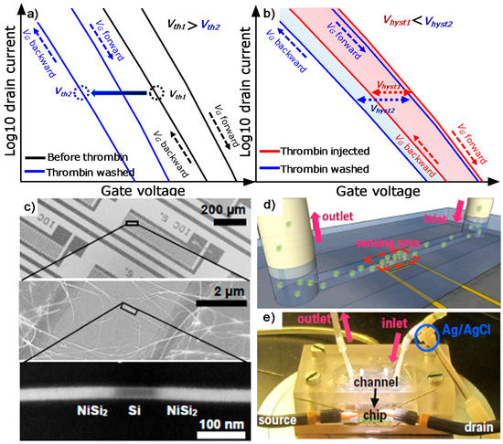
Figure 1.
(a) Schematic representation of expected shift of the transfer curve upon thrombin binding on the surface. (b) Expected shrinkage of the hysteresis in presence of thrombin in solution. (c) Details of the biosensor including microelectrodes and nanowires. Bottom panel shows the formed nickel silicide after the annealing process. (d) Concept depiction of the fluidic channel on the sensing area, and (e) fluidic assembly including mechanical clamping system, tubings, and electrical connections.
2. Materials and Methods
In order to fabricate such devices, a previously reported process was followed [32,33,42]. Nominally intrinsic, undoped silicon nanowires were grown by bottom-up means employing the vapor-liquid-solid (VLS) mechanism. SiO2 coated Si wafers were plasma activated and functionalized with poly(diallyldimethylammonium chloride) (PDDA) followed by deposition of gold nanoparticles of an average 19 nm in diameter to be used as seeds for the nanowire growth. PDDA ensures a high gold nanoparticle density with no aggregation. An additional plasma cleaning was applied to remove organic residues, preventing contamination of the nanowires. The substrates were heated to 450 °C in a chemical vapor deposition reactor in hydrogen atmosphere at 65 mbar. A SiH4/H2 (10/1 p/p) gas mixture was injected at 200 sccm for 15 min, which resulted in the growth of nanowires with 5–10 µm length and 22 nm diameter.
Using the nanowire growth substrate as donor, parallel arrangements of silicon nanowires were contact-printed onto a receiver Si wafer coated with a SiO2 layer for further chip fabrication. Source and drain electrodes in meander shaped patterns were formed by UV photo-lithography, sputter-deposition of nickel and lift-off in order to integrate a plurality of nanowire channels in parallel. The native oxide shell was removed from the nanowires prior to the nickel deposition by etching in buffered HF. This step is necessary since the oxide shell could block the diffusion of nickel in to the wire during the next silicidation step. The contact resistance at the silicon-nickel interfaces was dramatically reduced via thermal annealing at 500 °C in N2/H2 gas (10/1 p/p) and resulted in a NiSi2 intrusion into the Si nanowires (see Figure 1c).
A 15 nm-thick film of Al2O3 was deposited using atomic layer deposition (ALD) as a gate dielectric and as an ion-sensitive interface. Devices with close to ideal Nernstian sensitivity were obtained using this oxide material [32,43]. Each FET had up to 103 parallel nanowire channels. The sensing capabilities of similar devices in a liquid environment have been demonstrated recently by Zörgiebel et al. [32] for pH detection. Microchips of approximately 2 × 2 cm2 were mounted onto a microfluidic device consisting of a PMMA (polymethylmethacrylate) capillary tubing holder and an embedded PDMS (polydimethylsiloxane) channel with width of about 800 µm (see Figure 1d,e). After placing the PDMS channel above the sensitive NW region, the microchip was mechanically clamped to prevent leakage of the fluids. Ag/AgCl reference electrode (Microelectrodes Inc., USA) installed at the inlet tube assures it measures against a stable liquid potential. The transfer and output characteristics of the fabricated SiNW FET, exposed to a deionized (DI) water environment are represented in Figure 2a,b. The multi-silicon nanowire FET reveals p-type characteristics with a slight shift of the minimum current region towards positive gate voltages, which can be attributed to positive fixed charges arising by the stacking of Al2O3 on top of SiO2 [44]. Integration of devices into a portable fluidic system and the electrode isolation strategy described above permits long time robust sensing measurements in liquid environment. Up to 20 different multi-silicon nanowire FET devices are formed in a single chip, using the developed electrode design. This assures the presence of the suitable high performance ISFETs on a chip and would enable the integration in a multiplexing system to verify the reproducibility of the detection events, by measuring simultaneously different devices [45].
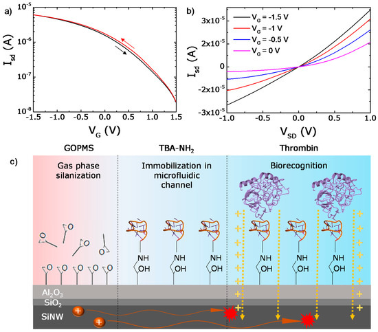
Figure 2.
(a) Semi logarithmic transfer characteristics and (b) output characteristics of the Si NW FETs. (c) Biochemical functionalization of the aluminum oxide surface. Glycidoxypropyltrimethoxysilane (GOPMS) was used as a linker molecule to covalently attach the aptamer via amino-alcohol bond formation. The further thrombin recognition by the aptamer leads to semiconducting channel modulation (dashed yellow arrows).
The design of the microfluidic assembly enables it to perform all the functionalization steps and detection events directly in the channel. All experiments were performed in-flow (Figure 1d,e), where the sample solution is injected at a constant flow rate of 100 μL/min with a syringe pump (PHD 2000, Harvard Apparatus, Holliston, MA, USA). The pump was stopped for 200 s after injection of samples for incubation. To realize the specific detection of thrombin, the surface of the sensor surface was prepared as follows. Glycidoxypropyltrimethoxysilane (GOPMS) with a reactive epoxy end group is used to attach amine-terminated strands of the thrombin-binding aptamer TBA (3′-GGTTGGTGTGGTTGG-T6-(CH2)6-NH2 -5′) via stable amino-alcohol bond formation, as sketched in Figure 2c. GOPMS covalently links to the Al2O3 layer via gas phase adsorption at elevated temperatures as described elsewhere [46]. We confirmed the binding using contact angle measurement (Contact Angle System OCA, DataPhysics, Filderstadt, Germany), dripping a water droplet on the Si-wafer as a control, indicating a homogeneously covered sample with a mean contact angle of 64 degrees compared to 36 degrees for the bare oxide. Further, surface characterization using gold nanoparticle labeling of functional groups and dripping the fluorescently labeled aptamers on the GOPMS surface using a nanoplotter confirmed the individual functionalization steps. The details of this confirmation can be found in the Supporting Information, Figure S1).
3. Results and Discussion
In the following we perform the detection of the thrombin concentrations in the range from 200 pM to 200 nM on a NW sensor surface, decorated with TBA. Further, we calibrate the concentrations values with the measured transfer curves of the FET in a sweeping gate mode; i.e., analyzing the thrombin dependent occurrence of the hysteresis in the device characteristics. Our developed measurement technique enables us to successfully implement and discuss such a concept for the first time. On the other hand, the thrombin-induced subthreshold voltage shifts dVT caused by increasing concentrations of biomolecules is presented as well. The latter represents a conventional approach used for calibration of the NW FET based sensors. Finally, we compare both analysis techniques in terms of their sensitivity and dynamic range.
3.1. Detection of Thrombin: Optimizing the Conditions
To achieve the measurable signal changes upon thrombin attachment, the experiments were performed in slightly acidic conditions with pH of about 5.7, based on the isoelectric point (pI) of thrombin (pI = 7.0–7.6, Haematologic Technologies, Inc., Essex Junction, VT, USA). The acidity of the solution thus ensures the positively charged state of the protein molecules are able to influence the surface potential of the NW FETs [25,26,47].
For the specific attachment of thrombin via the aptamers (Figure 2c), functionalization of the GOPMS modified sensor area was further performed by injecting the solution containing the TBA into the microfluidic channel, and left incubating for 20 min. A randomized control sequence (RDM, 3′-CATCCAACTGTCTCACAC-(CH2)6-NH2-5′) was immobilized on another NW FET as a nonspecific control test. After the removal of loosely attached strands, covalently bound DNA was incubated with 10 mM Tris buffer (pH 7.4) containing K+ ions to promote the proper folding of the aptamer structure [48,49,50]. Further, 1 mM pure sodium phosphate buffer (SPB) buffer at pH 5.7 was injected into the channel prior to detection experiments to establish the reference baseline for further experiments.
Finally, we inject the SPB buffer solutions with the different concentrations of thrombin into the channel step by step with the flow rate 100 μL/min. The infusion of each concentration was accompanied with a pumping pause during 200 s for the incubation purpose. Subsequent pumping of pure buffer removes loosely bound thrombin, while at the same time delivering the signal level (after rinse level). A concentration range from 200 pM to 200 nM of thrombin was tested in the following experiments.
3.2. Measurements Concept
A source meter (Keithley 2602, Tektronix, Köln, Germany) was used for voltage supply and current measurement of FET arrays. Source and drain electrodes were contacted via probe station needles. The gate was connected to the reference electrode and to the back-gate. The conventionally applied method for measuring the bioanalytes in NW FET is realized either with a fixed gate voltage VG or at fixed source drain current ISD using a feedback loop. In contrast, we monitored the signal changes in the FET by sweeping VG and recording source drain current ISD continuously at a sampling rate of around 50 data points per sweep [32]. The gate voltage resembles a triangular shaped signal with a frequency of about 1 Hz. The VG range was chosen such that the complete switching characteristic of the FET device was recorded in each sweep. The measurements were controlled by a Matlab-based program (The Mathworks Inc., Natick, MA, USA) for continuous monitoring of ISD and VG. This approach allows us to extract the threshold voltage shift dVT at a fixed ISD from the recorded data and to analyze its shift in real time. Compared to a feedback loop regulating a fixed ISD it delivers additional information on any possible change in shape of the I-V characteristics. This feature is specifically helpful in our proposed method since the separated analysis of the “positive” (from “+” to “−”) and “negative” (from “−” to “+”) branches of the sweep allows us to monitor evolution of the hysteresis in the transfer characteristics upon thrombin molecules loading. For the analysis purposes, we define the hysteresis width Vhyst via subtraction of positive and negative VG scans during live measuring of the transfer characteristics of the NW FET.
3.3. Hysteresis of the Transfer Curve Versus Subthreshold Shift dVT for Thrombin Detection
Figure 3a summarizes the thrombin sensing experiments upon the step by step addition of the thrombin molecules into the solution. It demonstrates the concurrent measurements of threshold voltage shift dVT (blue curve) and hysteresis evolution Vhyst (black curve) for the color-coded concentrations of thrombin (200 pM–200 nM) in a gate sweep measurement as a function of VG and time. The analyzed data allow us to make a number of conclusions discussed in detail below: (i) the fluid flow rate (on/off) influences the measurements dramatically; (ii) an irreversible dVT upon increase of thrombin concentration was observed; (iii) the (reversible) increase of hysteresis Vhyst was found to be dependent on thrombin concentration (Figure 3b,c). This is especially the case in the range of high analyte concentrations (nM range). The first aspect, related to the dependence of the sensor signal on the pumping rate, is eventually caused by the perturbation of the formed Debye layer; i.e., the removal of the diffusive outer layer in the electric double layer induced by the on/off operation of the fluidic pump injecting the analyte solutions (100 µL/min during buffer or thrombin injection followed by incubation in static state). Such effects were previously described for ion-sensitive field effect transistors (ISFETs) [51].
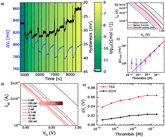
Figure 3.
Thrombin detection experiment with the bio-functionalized FET. (a) Real-time results upon step by step addition of thrombin, resulting in threshold voltage hysteresis (black line) and threshold voltage shift (blue line). (b) Example hysteretic transfer curves before thrombin addition, after thrombin injection and after rinsing. (c) Calibration of the hysteresis in the logarithmic scale of thrombin concentration. (d) Magnification of the transfer curves after different thrombin concentrations demonstrating an accumulative negative shift. (e) Calibration curve of the threshold voltage shift for thrombin detection using the TBA (red line) and the RDM (black line).
Subthreshold shift dVT for thrombin detection: Furthermore we analyze dVT upon addition of the thrombin into the solution. Magnified details of the corresponding ISD-VG curves are displayed in Figure 3d. It demonstrates the accumulation of the thrombin-induced voltage shifts upon increasing concentrations from 0 (lowest concentration tested: 200 pM) to 200 nM, from the right (buffer curve) to the left (maximal concentration 200 nM). Note the progressively smaller voltage shifts at higher concentrations of the injected thrombin, which is potentially attributed to a gradual saturation of binding sites on the sensor surface. To analyze dVTi induced by thrombin attachment, the corresponding VG at a fixed ISD at different times ti (with t = ti after thrombin attachment and rinsing for each concentration Ci) are determined at a level where the subthreshold slope is steepest in the semilogarithmic plot. Although this point is in the subthreshold regime and therefore below the conventional threshold of field effect transistors, we deliberately define this point of measurement as our sensor threshold voltage VT since there is only a constant offset to the point where the transistor actually turns on. The VT value is calculated as the mean value of both branches of the FET gating hysteresis at each time step. Apart from the instantaneous change of VT, we plot the fragments of the transfer characteristics, depicting the negative shift of the curve upon increase of the thrombin concentration from 0 (200 pM lowest concentration) to 200 nM (Figure 3d). For each dVT value at different thrombin concentrations, the running mean of 15 neighboring VT values is taken after the signal saturation and is averaged to flatten the curve, resulting in a small error bar of dVT of less than 1 mV. Figure 3e summarizes the dVT measurements and displays the calibration curve where the mean dVT is represented as a function of the thrombin concentration trapped by the specific TBA at the sensor surface (red line). Note that dVT is found to be significantly higher for the aptamer decorated surface compared to the negative control surface with RDM (red and black curves, respectively), indicating a primary specific interaction of TBA with thrombin, whereas the signal increase for the RDM functionalized surface is caused mainly by unspecific protein adsorption. In summary, the presented method enables the detection of the thrombin concentrations as low as 200 pM, which is within the range presented by other aptamer based FET sensors for thrombin detection [25,47]. The achieved sensitivity reaches approximately 10 mV/dec, which is also comparable to recently published SiNW-based FET biosensing using antibodies [52].
Hysteresis of the transfer curve: In contrast to the saturating threshold voltage, the measured hysteresis shows a distinct response on the thrombin concentration that is only slightly impeded by the fluid flow and, most importantly, is reversibly changing with thrombin concentration (see Figure 3a, black line). Instabilities in the real time signal might be explained by a reference potential drift. A stable Ag/AgCl reference electrode should be immersed in a solution with constant chloride concentration, while here it is in direct contact with buffer and sample solutions [53]. The estimated magnitude of the Vhyst shift is by a factor of five lower than that of the threshold voltage shift dVT. We analyzed the magnitude of the hysteresis shift and plotted the result as a function of thrombin concentration in Figure 3c. We fit the hysteresis and thrombin concentration data with a model describing the change of hysteresis with the square root of thrombin concentration. Fit inputs were the averaged data for constant thrombin concentration and the respective standard deviation. The fitted sensitivity was 2.15 nM/mV2, with a hysteresis offset for a zero thrombin concentration of −32.1 mV. Below 2 nM thrombin concentration the hysteresis is almost constant, while above that point the square root dependence is very clear.
We can explain the experimental evidence of a square root dependence of hysteresis and thrombin concentration with the dipole moment of thrombin molecules that is potentially changing with thrombin concentration in a square root dependence. We derive an explanation of this hypothesis starting on the description of hysteresis itself. Generally the initial hysteresis in the transfer cure is attributed to charge traps along the Si NW/SiO2 interface, with a trap filling and emptying process that requires time for equilibrium [54,55]. However, it can also be a result of time-dependent capacitive gating, producing variations in the effective VT and therefore in the hysteresis if the capacitance is changed at the dielectric layer and the ambient [56,57]. Altogether, measurable differences will be found for increasing and decreasing VG. While the Si NW/SiO2 traps are constant in our system, the explanation to hysteresis variations must be found on the thrombin itself in relation to capacitance changes. Since thrombin is positively charged in the hereby tested conditions, the binding due to the biorecognition process leaves a positively charged biomolecular layer on the FET surface, with the subsequent layer of attracted negative ions from the buffer solution. This results in a specific double-layer capacitance value. On the other hand, it is known that thrombin is a molecule that tends to be highly polarizable. [58]. An increasing dipole moment density at the surface leads to a diminishing double-layer and surface capacitance, as well as a modification of the hysteresis width. The dipole moment of surface bound molecules is therefore expected to have an influence on the hysteresis.
Certainly, the hysteresis is changed with the capacitance, which in turn can be changed by the dipole moment of molecules that bind to the surface. In addition, the dipole moment of the molecules can be changed by chemical means, thereby leading to a non-linear relation of molecular concentration and hysteresis change that is reversibly changing the hysteresis even when the surface is fully decorated with analyte molecules. We want to stress, that intrinsic FET hysteresis measured at a sweeping frequency of 1 Hz is completely independent of hysteresis with origins in the biorecognition process, which is measured over time scales of minutes up to hours. Our data shows no evidence of such sensor hysteresis drift that would render our sensing signal unusable. This makes measurements of the gate voltage hysteresis in BioFETs interesting for biological investigations in general.
Reference measurements: It has to be stressed that we performed a number of reference experiments with SiNW FETs and using complementary techniques to confirm and improve the efficiency of the biochemical approach, including the use of RDM instead of TBA at the sensor surface, as well as introducing the control protein TGF-β1 instead of thrombin [31]. In particular, the previous fluorescence based bioanalytic assays have confirmed the binding of thrombin on TBA surfaces, prepared with identical functionalization approach [31]. Furthermore, the additional surface-regeneration step for this aptamer-target system aimed to separate the two biorecognition partners in an efficient manner [49,59] was implemented using NaOH in quartz crystal microbalance technique (QCM, Figure S2), and obtaining saturation levels after 270 nM thrombin, in agreement with previous findings [31] and other publications [60,61].This important step could be further integrated into the SiNW FET concept to increase the lifetime of the microchips by recycling.
4. Conclusions
In conclusion, we present a thrombin detection platform using large area multiwire FET devices, relying on the live monitoring of the transfer curves in the gate sweeping regime. Remarkably, these dynamic sweeping measurements allowed us to observe the occurrence and the further evolution of the transfer curve hysteresis once the thrombin molecules bind to the sensor surface. While attributing the hysteresis appearance to the dipolar moment of thrombin, we for the first time implement the hysteresis width as a reliable parameter to control and calibrate the concentration of biomolecules forming dipoles in solution.
While the traditional detection by threshold voltage shift is capable of performing the biosensing starting in the picomolar range, the new method based on the hysteresis could be useful for the quantification of polarizable molecules that are found in nanomolar concentrations as well as for the analysis of the polarization behavior. We demonstrate that the hysteresis-based analysis allows us to detect thrombin in the nanomolar range, and can be a sensitive measure for molecules with a dipole moment, but with little net charge. The quantification of the subthreshold voltage shift decreases the detectable range by almost one order of magnitude (smallest detected concentration is 200 pM), allowing us to increase the sensitivity if needed.
While the traditional detection by threshold voltage shift in ISFETs is capable of performing biosensing starting in the picomolar range (smallest detected concentration in our work is 200 pM), the new method based on the hysteresis could be useful for the quantification down to nanomolar concentrations. No saturation was observed with the gate hysteresis technique in the measured range, meaning that even higher concentrations might be possible to be detected. We further demonstrate that the hysteresis-based analysis can be a sensitive measure for molecules with a dipole moment, but little net charge, broadening the range of biomolecular species that can be detected, beyond the traditional electrically charged ones using the voltage shift technique. The analysis of the polarization behavior is also enabled.
Further application of the hysteresis technique in real time samples remains to be tested with a surface modification involving polyethylene glycol that allows increasing the effective Debye length [62,63,64]. The indication of certain diseases can also be further improved by using several bioreceptors and neural networks for fingerprinting of the samples [65,66].
Supplementary Materials
The following are available online at http://www.mdpi.com/2076-3417/8/6/950/s1, Figure S1: Characterization of the biochemical functionalization steps, Figure S2: Quartz-crystal microbalance monitoring of the biorecognition process.
Author Contributions
L.B. and G.C. conceived and designed the experiments; B.I., L.R., F.Z., S.P. and M.V. performed the experimental work and analyzed the data under the supervision of W.M.W., T.M., J.O., L.B. and G.C. B.I., L.R. and L.B. wrote the paper with feedback from all authors.
Acknowledgments
This work was supported by the European Union (European Social Fund) and the Free State of Saxony (Sächsische Aufbaubank) in the young researcher group ‘InnovaSens’ (SAB-Nr. 080942409). Further we acknowledge support from the German Excellence Initiative via the Cluster of Excellence EXC1056 “Center for Advancing Electronics Dresden” (cfAED).
Conflicts of Interest
The authors declare no conflict of interest.
References
- Drain, P.K.; Hyle, E.P.; Noubary, F.; Freedberg, K.A.; Wilson, D.; Bishai, W.R.; Rodriguez, W.; Bassett, I.V. Diagnostic point-of-care tests in resource-limited settings. Lancet Infect. Dis. 2014, 14, 239–249. [Google Scholar] [CrossRef]
- Kulinsky, L.; Noroozi, Z.; Madou, M. Present technology and future trends in point-of-care microfluidic diagnostics. Methods Mol. Biol. 2013, 949, 3–23. [Google Scholar] [CrossRef] [PubMed]
- United Nations, Department of Economic and Social Affairs. World Population Ageing; United Nations Report 2013; Report No.: ST/ESA/SER.A/348; United Nations: New York, NY, USA, 2013; Volume 114. [Google Scholar]
- Chin, C.D.; Laksanasopin, T.; Cheung, Y.K.; Steinmiller, D.; Linder, V.; Parsa, H.; Wang, J.; Moore, H.; Rouse, R.; Umviligihozo, G.; et al. Microfluidics-based diagnostics of infectious diseases in the developing world. Nat. Med. 2011, 17, 1015–1019. [Google Scholar] [CrossRef] [PubMed]
- Hopfer, S.M.; Nadeau, F.L.; Sundra, M.; Makowski, G.S. Effect of Protein on Hemoglobin and Hematocrit Assays with a Conductivity-Based Point-of-Care Testing Device: Comparison with Optical Methods. Ann. Clin. Lab. Sci. 2004, 34, 75–82. [Google Scholar] [PubMed]
- Flegar-Meštrić, Z.; Perkov, S. Comparability of point-of-care whole-blood electrolyte and substrate testing using a Stat Profile Critical Care Xpress analyzer and standard laboratory methods. Clin. Chem. Lab. Med. 2006, 44, 898–903. [Google Scholar] [CrossRef] [PubMed]
- St John, A.; Price, C.P. Existing and Emerging Technologies for Point-of-Care Testing. Clin. Biochem. Rev. 2014, 35, 155–167. [Google Scholar] [PubMed]
- Karnaushenko, D.; Ibarlucea, B.; Lee, S.; Lin, G.; Baraban, L.; Pregl, S.; Melzer, M.; Makarov, D.; Weber, W.M.; Mikolajick, T.; et al. Light Weight and Flexible High-Performance Diagnostic Platform. Adv. Healthc. Mater. 2015, 4, 1517–1525. [Google Scholar] [CrossRef] [PubMed]
- Sista, R.; Hua, Z.; Thwar, P.; Sudarsan, A.; Srinivasan, V.; Eckhardt, A.; Pollack, M.; Pamula, V. Development of a digital microfluidic platform for point of care testing. Lab Chip 2008, 8, 2091–2104. [Google Scholar] [CrossRef] [PubMed]
- Ferguson, B.S.; Buchsbaum, S.F.; Wu, T.T.; Hsieh, K.; Xiao, Y.; Sun, R.; Soh, H.T. Genetic analysis of H1N1 influenza virus from throat swab samples in a microfluidic system for point-of-care diagnostics. J. Am. Chem. Soc. 2011, 133, 9129–9135. [Google Scholar] [CrossRef] [PubMed]
- Gao, A.; Lu, N.; Dai, P.; Li, T.; Pei, H.; Gao, X.; Gong, Y.; Wang, Y.; Fan, C. Silicon-nanowire-based CMOS-compatible field-effect transistor nanosensors for ultrasensitive electrical detection of nucleic acids. Nano Lett. 2011, 11, 3974–3978. [Google Scholar] [CrossRef] [PubMed]
- Baraban, L.; Zörgiebel, F.; Pahlke, C.; Baek, E.; Römhildt, L.; Cuniberti, G. Lab on a Wire: Application of Silicon Nanowires for Nanoscience and Biotechnology. In Nanowire Field Effect Transistors: Principles and Applications; Springer: New York, NY, USA, 2014; pp. 241–278. [Google Scholar]
- Giljohann, D.A.; Mirkin, C.A. Drivers of biodiagnostic development. Nature 2009, 462, 461–464. [Google Scholar] [CrossRef] [PubMed]
- Patolsky, F.; Zheng, G.; Lieber, C.M. Nanowire sensors for medicine and the life sciences. Nanomedicine 2006, 1, 51–65. [Google Scholar] [CrossRef] [PubMed]
- Gao, X.P.A.; Zheng, G.; Lieber, C.M. Subthreshold regime has the optimal sensitivity for nanowire FET biosensors. Nano Lett. 2010, 10, 547–552. [Google Scholar] [CrossRef] [PubMed]
- Baek, E.; Rim, T.; Schütt, J.; Baek, C.; Kim, K.; Baraban, L.; Cuniberti, G. Negative Photoconductance in Heavily Doped Si Nanowire Field-Effect Transistors. Nano Lett. 2017, 17, 6727–6734. [Google Scholar] [CrossRef] [PubMed]
- Meyyappan, M.; Sunkara, M. Inorganic Nanowires Applications, Properties, and Characterization; CRC Press: Boca Raton, FL, USA, 2009; ISBN 9781420067835. [Google Scholar]
- Park, C.W.; Ah, C.S.; Ahn, C.G.; Yang, J.H.; Kim, A.; Kim, T.Y.; Sung, G.Y. Analysis of configuration of surface-immobilized proteins by Si nanochannel field effect transistor biosensor. Sens. Actuators B Chem. 2011, 154, 164–168. [Google Scholar] [CrossRef]
- Weber, W.M.; Mikolajick, T. Silicon and germanium nanowire electronics: Physics of conventional and unconventional transistors. Rep. Prog. Phys. 2017, 80, 066502. [Google Scholar] [CrossRef] [PubMed]
- Elnathan, R.; Kwiat, M.; Pevzner, A.; Engel, Y.; Burstein, L.; Khatchtourints, A.; Lichtenstein, A.; Kantaev, R.; Patolsky, F. Biorecognition layer engineering: Overcoming screening limitations of nanowire-based FET devices. Nano Lett. 2012, 12, 5245–5254. [Google Scholar] [CrossRef] [PubMed]
- Hahm, J.; Lieber, C.M. Direct Ultrasensitive Electrical Detection of DNA and DNA Sequence Variations Using Nanowire Nanosensors. Nano Lett. 2004, 4, 51–54. [Google Scholar] [CrossRef]
- Chiu, T.C.; Huang, C.C. Aptamer-functionalized nano-biosensors. Sensors 2009, 9, 10356–10388. [Google Scholar] [CrossRef] [PubMed]
- O’Sullivan, C.K. Aptasensors--the future of biosensing? Anal. Bioanal. Chem. 2002, 372, 44–48. [Google Scholar] [CrossRef] [PubMed]
- Mascini, M. Aptamers in Bioanalysis; John Wiley & Sons: Hoboken, NJ, USA, 2009; ISBN 9780470148303. [Google Scholar]
- Kim, K.S.; Lee, H.-S.; Yang, J.-A.; Jo, M.-H.; Hahn, S.K. The fabrication, characterization and application of aptamer-functionalized Si-nanowire FET biosensors. Nanotechnology 2009, 20, 235501. [Google Scholar] [CrossRef] [PubMed]
- Römhildt, L.; Zörgiebel, F.; Ibarlucea, B.; Vahdatzadeh, M.; Baraban, L.; Cuniberti, G.; Pregl, S.; Weber, W.M.; Mikolajick, T.; Opitz, J. Human α-thrombin detection platform using aptamers on a silicon nanowire field-effect transistor. In Proceedings of the 2017 27th International Symposium on Power and Timing Modeling, Optimization and Simulation (PATMOS), Thessaloniki, Greece, 25–27 September 2017; IEEE: Piscataway, NJ, USA, 2017; pp. 1–4. [Google Scholar]
- Anand, A.; Liu, C.-R.; Chou, A.-C.; Hsu, W.-H.; Ulaganathan, R.K.; Lin, Y.-C.; Dai, C.-A.; Tseng, F.-G.; Pan, C.-Y.; Chen, Y.-T. Detection of K+ Efflux from Stimulated Cortical Neurons by an Aptamer-Modified Silicon Nanowire Field-Effect Transistor. ACS Sens. 2017, 2, 69–79. [Google Scholar] [CrossRef] [PubMed]
- Li, B.R.; Hsieh, Y.J.; Chen, Y.X.; Chung, Y.T.; Pan, C.Y.; Chen, Y.T. An ultrasensitive nanowire-transistor biosensor for detecting dopamine release from living pc12 cells under hypoxic stimulation. J. Am. Chem. Soc. 2013, 135, 16034–16037. [Google Scholar] [CrossRef] [PubMed]
- Lee, H.S.; Kim, K.S.; Kim, C.J.; Hahn, S.K.; Jo, M.H. Electrical detection of VEGFs for cancer diagnoses using anti-vascular endotherial growth factor aptamer-modified Si nanowire FETs. Biosens. Bioelectron. 2009, 24, 1801–1805. [Google Scholar] [CrossRef] [PubMed]
- Centi, S.; Tombelli, S.; Minunni, M.; Mascini, M. Aptamer-based detection of plasma proteins by an electrochemical assay coupled to magnetic beads. Anal. Chem. 2007, 79, 1466–1473. [Google Scholar] [CrossRef] [PubMed]
- Römhildt, L.; Pahlke, C.; Zörgiebel, F.; Braun, H.G.; Opitz, J.; Baraban, L.; Cuniberti, G. Patterned biochemical functionalization improves aptamer-based detection of unlabeled thrombin in a sandwich assay. ACS Appl. Mater. Interfaces 2013, 5, 12029–12035. [Google Scholar] [CrossRef] [PubMed]
- Zörgiebel, F.M.; Pregl, S.; Römhildt, L.; Opitz, J.; Weber, W.; Mikolajick, T.; Baraban, L.; Cuniberti, G. Schottky barrier-based silicon nanowire pH sensor with live sensitivity control. Nano Res. 2014, 7, 263–271. [Google Scholar] [CrossRef]
- Pregl, S.; Weber, W.M.; Nozaki, D.; Kunstmann, J.; Baraban, L.; Opitz, J.; Mikolajick, T.; Cuniberti, G. Parallel arrays of Schottky barrier nanowire field effect transistors: Nanoscopic effects for macroscopic current output. Nano Res. 2013, 6, 381–388. [Google Scholar] [CrossRef]
- Schütt, J.; Ibarlucea, B.; Illing, R.; Zörgiebel, F.; Pregl, S.; Nozaki, D.; Weber, W.M.; Mikolajick, T.; Baraban, L.; Cuniberti, G. Compact Nanowire Sensors Probe Microdroplets. Nano Lett. 2016, 16. [Google Scholar] [CrossRef] [PubMed]
- Baek, E.; Pregl, S.; Shaygan, M.; Römhildt, L.; Weber, W.M.; Mikolajick, T.; Ryndyk, D.A.; Baraban, L.; Cuniberti, G. Optoelectronic switching of nanowire-based hybrid organic/oxide/semiconductor field-effect transistors. Nano Res. 2015, 8, 1229–1240. [Google Scholar] [CrossRef]
- Regonda, S.; Tian, R.; Gao, J.; Greene, S.; Ding, J.; Hu, W. Silicon multi-nanochannel FETs to improve device uniformity/stability and femtomolar detection of insulin in serum. Biosens. Bioelectron. 2013, 45, 245–251. [Google Scholar] [CrossRef] [PubMed]
- Gong, X.; Zhao, R.; Yu, X. High sensitive detections of Norovirus DNA and IgG by using multi-SiNW-FET biosensors. In Proceedings of the 18th International Conference on Solid-State Sensors, Actuators and Microsystems (Transducers 2015), Anchorage, AK, USA, 21–25 June 2015; pp. 1537–1540. [Google Scholar]
- Paska, Y.; Haick, H. Interactive effect of hysteresis and surface chemistry on gated silicon nanowire gas sensors. ACS Appl. Mater. Interfaces 2012, 4, 2604–2617. [Google Scholar] [CrossRef] [PubMed]
- Puppo, F.; Traversa, F.L.; De Ventra, M.; De Micheli, G.; Carrara, S. Surface trap mediated electronic transport in biofunctionalized silicon nanowires. Nanotechnology 2016, 27. [Google Scholar] [CrossRef] [PubMed]
- Ibarlucea, B.; Fawzul Akbar, T.; Kim, K.; Rim, T.; Baek, C.-K.; Ascoli, A.; Tetzlaff, R.; Baraban, L.; Cuniberti, G. Ultrasensitive detection of Ebola matrix protein in a memristor mode. Nano Res. 2018, 11, 1057–1068. [Google Scholar] [CrossRef]
- Tarasov, A.; Wipf, M.; Bedner, K.; Kurz, J.; Fu, W.; Guzenko, V.A.; Knopfmacher, O.; Stoop, R.L.; Calame, M.; Schönenberger, C. True reference nanosensor realized with silicon nanowires. Langmuir 2012, 28, 9899–9905. [Google Scholar] [CrossRef] [PubMed]
- Mikolajick, T.; Weber, W.M. Silicon Nanowires: Fabrication and Applications. In Anisotropic Nanomaterials; Li, Q., Ed.; Springer: New York, NY, USA, 2015; pp. 1–25. [Google Scholar]
- Wipf, M.; Stoop, R.L.; Tarasov, A.; Bedner, K.; Fu, W.; Wright, I.A.; Martin, C.J.; Constable, E.C.; Calame, M.; Schönenberger, C. Selective sodium sensing with gold-coated silicon nanowire field-effect transistors in a differential setup. ACS Nano 2013, 7, 5978–5983. [Google Scholar] [CrossRef] [PubMed]
- Simon, D.K.; Jordan, P.M.; Mikolajick, T.; Dirnstorfer, I. On the Control of the Fixed Charge Densities in Al2O3-Based Silicon Surface Passivation Schemes. ACS Appl. Mater. Interfaces 2015, 7, 28215–28222. [Google Scholar] [CrossRef] [PubMed]
- Voitsekhivska, T.; Zorgiebel, F.; Suthau, E.; Wolter, K.-J.; Bock, K.; Cuniberti, G. pH measurements of FET-based (bio)chemical sensors using portable measurement system. In Proceedings of the 2015 37th Annual International Conference of the IEEE Engineering in Medicine and Biology Society (EMBC), Milano, Italy, 25–29 August 2015; IEEE: Piscataway, NJ, USA, 2015; Volume 2015, pp. 6445–6448. [Google Scholar]
- Ingebrandt, S.; Vu, X.T.; Eschermann, J.F.; Stockmann, R.; Offenhäusser, A. Top-Down Processed SOI Nanowire Devices for Biomedical Applications. ECS Trans. 2011, 35, 3–15. [Google Scholar] [CrossRef]
- Hammock, M.L.; Knopfmacher, O.; Naab, B.D.; Tok, J.B.H.; Bao, Z. Investigation of protein detection parameters using nanofunctionalized organic field-effect transistors. ACS Nano 2013, 7, 3970–3980. [Google Scholar] [CrossRef] [PubMed]
- Baldrich, E.; Restrepo, A.; O’Sullivan, C.K. Aptasensor development: Elucidation of critical parameters for optimal aptamer performance. Anal. Chem. 2005, 76, 7053–7063. [Google Scholar] [CrossRef] [PubMed]
- Henseleit, A.; Schmieder, S.; Bley, T.; Sonntag, F.; Schilling, N.; Quenzel, P.; Danz, N.; Klotzbach, U.; Boschke, E. A compact and rapid aptasensor platform based on surface plasmon resonance. Eng. Life Sci. 2011, 11, 573–579. [Google Scholar] [CrossRef]
- Russo Krauss, I.; Merlino, A.; Randazzo, A.; Novellino, E.; Mazzarella, L.; Sica, F. High-resolution structures of two complexes between thrombin and thrombin-binding aptamer shed light on the role of cations in the aptamer inhibitory activity. Nucleic Acids Res. 2012, 40, 8119–8128. [Google Scholar] [CrossRef] [PubMed]
- Kim, D.R.; Lee, C.H.; Zheng, X. Probing flow velocity with silicon nanowire sensors. Nano Lett. 2009, 9, 1984–1988. [Google Scholar] [CrossRef] [PubMed]
- Rim, T.; Kim, K.; Hong, N.; Ko, W.; Baek, C.-K.; Jeon, S.; Deen, M.J.; Meyyappan, M.; Jeong, Y.-H.; Lee, J.-S. Investigation of the electrical stability of Si-nanowire biologically sensitive field-effect transistors with embedded Ag/AgCl pseudo reference electrode. RSC Adv. 2013, 3, 7963. [Google Scholar] [CrossRef]
- Kinlen, P.J.; Heider, J.E.; Hubbard, D.E. A solid-state ph sensor-based on a nafion-coated iridium oxide indicator electrode and a polymer-based silver-chloride reference electrode. Sens. Actuators B-Chem. 1994, 22, 13–25. [Google Scholar] [CrossRef]
- Rajeev, K.P.; Opoku, C.; Stolojan, V.; Constantinou, M.; Shkunov, M. Effect of Nanowire-dielectric Interface on the Hysteresis of Solution Processed Silicon Nanowire FETs. Nanosci. Nanoeng. 2017, 5, 17–24. [Google Scholar] [CrossRef]
- Fahem, Z.; Csaba, G.; Erlen, C.M.; Lugli, P.; Weber, W.M.; Geelhaar, L.; Riechert, H. Analysis of the hysteretic behavior of silicon nanowire transistors. Phys. Status Solidi Curr. Top. Solid State Phys. 2008, 5, 27–30. [Google Scholar] [CrossRef]
- Park, Y.; Baac, H.W.; Heo, J.; Yoo, G. Thermally activated trap charges responsible for hysteresis in multilayer MoS2field-effect transistors. Appl. Phys. Lett. 2016, 108. [Google Scholar] [CrossRef]
- Singh, M.; Manoli, K.; Tiwari, A.; Ligonzo, T.; Di Franco, C.; Cioffi, N.; Palazzo, G.; Scamarcio, G.; Torsi, L. The double layer capacitance of ionic liquids for electrolyte gating of ZnO thin film transistors and effect of gate electrodes. J. Mater. Chem. C 2017, 5, 3509–3518. [Google Scholar] [CrossRef]
- Fuglestad, B.; Gasper, P.M.; Tonelli, M.; McCammon, J.A.; Markwick, P.R.L.; Komives, E.A. The dynamic structure of thrombin in solution. Biophys. J. 2012, 103, 79–88. [Google Scholar] [CrossRef] [PubMed]
- Pasternak, A.; Hernandez, F.J.; Rasmussen, L.M.; Vester, B.; Wengel, J. Improved thrombin binding aptamer by incorporation of a single unlocked nucleic acid monomer. Nucleic Acids Res. 2011, 39, 1155–1164. [Google Scholar] [CrossRef] [PubMed]
- Hianik, T.; Ostatná, V.; Zajacová, Z.; Stoikova, E.; Evtugyn, G. Detection of aptamer-protein interactions using QCM and electrochemical indicator methods. Bioorgan. Med. Chem. Lett. 2005, 15, 291–295. [Google Scholar] [CrossRef] [PubMed]
- Cho, E.J.; Collett, J.R.; Szafranska, A.E.; Ellington, A.D. Optimization of aptamer microarray technology for multiple protein targets. Anal. Chim. Acta 2006, 564, 82–90. [Google Scholar] [CrossRef] [PubMed]
- Gao, N.; Zhou, W.; Jiang, X.; Hong, G.; Fu, T.M.; Lieber, C.M. General strategy for biodetection in high ionic strength solutions using transistor-based nanoelectronic sensors. Nano Lett. 2015, 15, 2143–2148. [Google Scholar] [CrossRef] [PubMed]
- Filipiak, M.S.; Rother, M.; Andoy, N.M.; Knudsen, A.C.; Grimm, S.B.; Bachran, C.; Swee, L.K.; Zaumseil, J.; Tarasov, A. Label-Free Immunodetection in High Ionic Strength Solutions Using Carbon Nanotube Transistors with Nanobody Receptors. Proceedings 2017, 1, 491. [Google Scholar] [CrossRef]
- Gutiérrez-Sanz, Ó.; Andoy, N.M.; Filipiak, M.S.; Haustein, N.; Tarasov, A. Direct, Label-Free, and Rapid Transistor-Based Immunodetection in Whole Serum. ACS Sens. 2017, 2, 1278–1286. [Google Scholar] [CrossRef] [PubMed]
- Wang, B.; Cancilla, J.C.; Torrecilla, J.S.; Haick, H. Artificial sensing intelligence with silicon nanowires for ultraselective detection in the gas phase. Nano Lett. 2014, 14, 933–938. [Google Scholar] [CrossRef] [PubMed]
- Shehada, N.; Cancilla, J.C.; Torrecilla, J.S.; Pariente, E.S.; Brönstrup, G.; Christiansen, S.; Johnson, D.W.; Leja, M.; Davies, M.P.A.; Liran, O.; et al. Silicon Nanowire Sensors Enable Diagnosis of Patients via Exhaled Breath. ACS Nano 2016, 10, 7047–7057. [Google Scholar] [CrossRef] [PubMed]


© 2018 by the authors. Licensee MDPI, Basel, Switzerland. This article is an open access article distributed under the terms and conditions of the Creative Commons Attribution (CC BY) license (http://creativecommons.org/licenses/by/4.0/).