Abstract
The convection thermal coupling between adjacent power devices in power converters is dependent on the ambient temperature. When the ambient temperature changes, the convection thermal coupling also changes. This results in an inaccurate thermal model that causes errors in the prediction of the thermal distribution and junction temperature based on a fixed ambient temperature for power devices in converters application. To solve this variable-ambient-temperature-related issue, a thermal coupling experiment for semiconductor power devices (the MOSFET and diode) was performed to discuss the influence of the thermal coupling effect between adjacent devices and the FEM (Finite Element Method) thermal models for the power devices considering the convection thermal coupling are established. Through these simulations, the junction temperatures of devices under different ambient temperatures were obtained, and the relationships between the junction temperature and ambient temperatures were established. Moreover, the junction temperatures of power devices under different ambient temperatures were calculated and temperature distributions are analyzed in this paper. This method shows a strong significance and has potential applications for high-efficiency and high-power density converter designs.
1. Introduction
1.1. Literature Review
The existing thermal analysis models [1,2] are often based on fixed ambient temperature values, such as 25 °C or 30 °C [3,4]. However, the ambient temperature is widely variable [5,6]. Different ambient temperatures have different effects on the convection thermal coupling between power devices [7,8]. Meanwhile, the convection thermal coupling also changes the temperature distribution and junction temperature of devices [9,10]. When the ambient temperature changes, the traditional thermal analysis models for power devices may cause errors to calculate the temperature distribution and junction temperature prediction [11,12].
The calculation formula of junction temperature is derived in [3] which considers the conduction thermal coupling effect while the derivation is based on a fixed ambient temperature and the analysis is based on the ideal air region. Here the parameters and ambient temperature are considered independent of the temperature, while the ambient temperatures are not constant, and the parameters are ambient temperature dependent.
The short-term and long-term electro-thermal models are analyzed in [6], and the long-term one is considered to be affected by the ambient temperature. Moreover, the junction and case temperatures of power devices can be estimated by these models. The device model estimates the voltage drop and switching energy of the device by considering the device current, the blocking voltage of the off state and the junction temperature change. The thermal models consider the conduction thermal coupling between MOSFETs and diodes integrated with the same package and the effect of the junction temperature of devices at the ambient temperatures of 25 °C and 30 °C. In this reference, it is pointed out that different ambient temperatures have different influences on the thermal coupling and the junction temperature, while only two ambient temperature points are considered, and the mentioned thermal model is only for one power device.
In [13], the dynamic ambient profile is analyzed, and a thermal analysis model based on the profile is established, while the thermal coupling effect among power devices in the system is not considered [14]. In the electrical grid network where the power devices are commonly located in the outdoor environment and the ambient temperature is not constant as discussed in [15].
The self-thermal resistance (case-to-ambient thermal resistance, Rca) of the power devices, the measured values of Rca in the datasheet in [16] show that the value will vary from the range of 190 °C/W to 310 °C/W [17] when the devices packaged with SO-8 with different forms of a substrate (P-DSO-14-4 and P-TO252-3-1) insulate. Meanwhile, the manufacturer, Infineon, has provided the variation curves for the junction-to-ambient thermal resistance (Rja) packaged under the two conditions of natural convection and forced air cooling, which indicates that the Rca is variable and the values depend on the package, working conditions and the boundary conditions.
Therefore, different ambient temperatures analysis will help the thermal coupling between power devices be better well-analyzed which can decrease the erroneous junction temperature calculation [18,19,20] and a better understanding of the ambient which is one of the important factors of the thermal coupling calculation can assist the practical design guidelines for impact power converters.
1.2. Main Contributions
The major contributions of this paper are as follows: thermal coupling experiment for semiconductor power devices (the MOSFET and diode) is performed to discuss the influence of thermal coupling effect between adjacent devices; FEM models for power devices considering convection thermal coupling are established; the junction temperatures of devices under different ambient temperatures and the temperature distribution have been given; and the relationships between junction temperature and ambient temperatures are obtained.
1.3. Outline
The paper is organized as follows. First, the variation of the ambient temperature after the analysis of the thermal transfer process and thermal coupling experiment to show the influence of the thermal coupling effect between adjacent devices is discussed in Section 2. Thermal models and FEM simulations for adjacent power devices considering convection thermal coupling are established in Section 3. The relationships between junction temperatures and ambient temperatures are presented in Section 4. After that, thermal models in new ambient temperatures are built to verify the proposed model in Section 5. Finally, the main conclusion is drawn in Section 6.
2. Variation of Ambient Temperature
2.1. Thermal Transfer Process
The thermal transfer process refers to the process that the thermal is transferred from the interior of the solid to the other side of the fluid through the solid wall, that is, the thermal transfers from the heating solid (chip) to the surrounding air, as shown in Figure 1. In the figure, tw1, tw2, tf are the temperatures and h is the convection coefficient. It is assumed that tw1, tw2, tf and h do not change with time and λ is a constant [21].
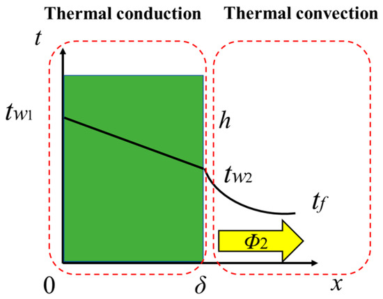
Figure 1.
Thermal transfer.
The thermal conduction equation of a flat wall can be obtained based on the steady-state thermal transfer
Furthermore, the thermal convection equation can be expressed as
When the thermal transfer reaches a steady state, it can be obtained by energy conservation
That is
where Rk is the total thermal transfer resistance, is conduction thermal resistance and Rh is convection thermal resistance.
Based on the theory of electrical to thermal, as shown in Figure 2: the resistance corresponds to the thermal resistance; the voltage difference corresponds to the temperature difference and the current corresponds to the power loss. The corresponding thermal resistance network in the thermal transfer process is shown in Figure 3.
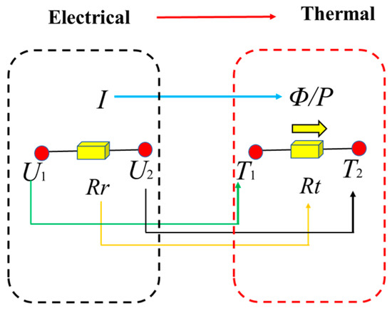
Figure 2.
The theory of electrical to thermal.
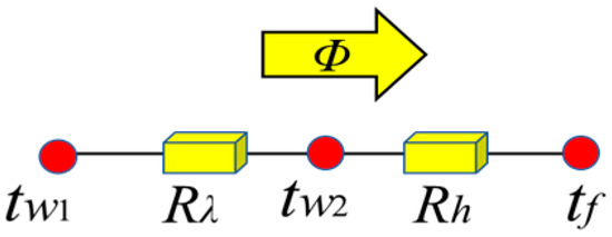
Figure 3.
Thermal resistance network.
2.2. Thermal Coupling Experiments
In this section, a thermal coupling testing platform for the power converter is established as shown in Figure 4, and its circuit diagram is shown in Figure 5. In this experimental platform, the selected switching frequencies of the power converters are commonly used, which are 10 kHz, 25 kHz and 50 kHz, respectively. The duty cycle is set to 0.5, and the load resistances are 8 Ω, 6 Ω and 5 Ω, respectively. The type of the power device MOSFET is IRF540 NPBF, the diode model is MBR20100CT, and both the semiconductor devices are in the TO-220 package. The capacitor is MAL215050472E3-35 V and the value of its capacitance is 4700 UF. The inductance is MCAP115018047A and the value of its inductance is 250 μH.
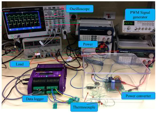
Figure 4.
Thermal coupling testing platform of the power converter.
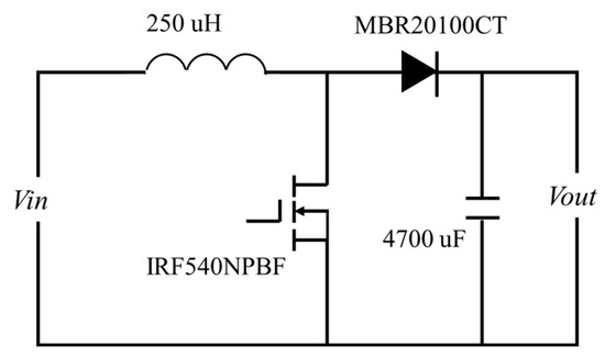
Figure 5.
The circuit diagram of the power converter.
In order to study the influence of the thermal coupling effect (the convection thermal coupling and conduction thermal coupling are included) of adjacent devices under different working conditions, the two different types of power converters are tested and compared as follows, type I with large device spacing and type II with small device spacing, as shown in Figure 6. The MOSFET is controlled by the PWM wave and its on state and off state are controlled by the given duty cycle and switching frequencies. During the testing of the converter system, the input voltage and output voltage of the circuit is 12 V and 24 V, respectively. The case temperature of the power devices of the converter system is collected by changing the load resistances.
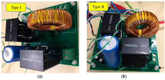
Figure 6.
Two different types of power converters: (a) type I with large device spacing; (b) type II with small device spacing.
Figure 7 shows the measurement results of the case temperatures and the calculation results of the temperature difference of the two power devices with different types of spacing. In this figure, the case temperature of the MOSFET and diode with two types of devices spacing (type I: large spacing, dot mark on the blue and cyan solid line; type II: small spacing, six-star mark on red and green solid line) are compared at the switching frequency of 25 kHz and the load resistances which are 8 Ω, 6 Ω and 5 Ω, respectively.
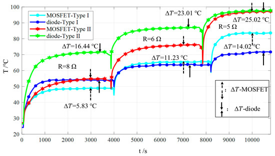
Figure 7.
The comparisons of the case temperatures and the temperature differences of the power devices with different spacing types.
It can be seen from the comparisons that, for both MOSFET and diode, with the decrease in device spacing the case temperature of the device increases under the same working condition. This shows that the thermal coupling effect between adjacent devices is affected by the device spacing, and with the decrease in the spacing, the thermal coupling effect increases. In addition, according to the comparison results of the case temperature difference in Table 1, when the load resistance decreases, the current flowing through the semiconductor device increases. At this time, the case temperature difference of the two devices changes with the change of current, which shows that the thermal coupling effect between adjacent devices is affected by the working current, and with the increase in the current the thermal coupling effect increases. It is verified that the thermal coupling effect obtained from the thermal coupling testing platform (the MOSFET and diode are tested) of devices can also be applied to the case where multiple devices exist in the power converter system.

Table 1.
The temperature differences of case temperature under different load resistances.
The calculation formula of the steady-state case-to-ambient thermal resistance, Rca in the convection thermal transfer is obtained as
The steady-state thermal resistance of the devices under different working conditions is analyzed. By bringing the measured steady-state Tc into (5), the Rca of the MOSFET and diode can be obtained. The calculation results are shown in Table 2 and Table 3, respectively. According to the two tables above, when the power loss (the working current) increases and the Tc rises, the values of Rca decrease. This shows that the Rca is not constant, and its value depends on the power loss and environmental factors.
Table 2.
Rca for the MOSFET.
Table 3.
Rca for the diode.
2.3. Finite Element Method (FEM) models
Thermal dissipation has a negative impact on the performance and lifetime of semiconductor devices and power converters. As shown in Figure 8, different colors constitute the thermal map and this simulation can be used to obtain the junction temperature (Tj) and case temperature (Tc), and the temperature at the chip and copper substrate layer is the highest.
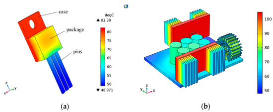
Figure 8.
FEM thermal analysis model: (a) three-dimensional thermal calculation model for a MOSFET; (b) temperature distributions of a power converter.
Therefore, thermal analysis modeling under different load conditions is essential, and it is necessary to seek the temperature calculation methods of power converters and the optimal distribution schemes of thermal distribution. As the size of a single traditional silicon-based device approaches its basic limit, a better understanding of the thermal distribution of adjacent devices under different operating conditions can help the system carry out reasonable thermal management, thus improving the performance of the converter system, and optimizing the overall structure of the converter [22]. The accuracy of the thermal analysis model has a significant impact on the thermal management and reliability of devices and systems.
For semiconductor devices and power converter systems, the commonly used thermal modeling methods mainly include the physical model calculation method, numerical calculation method, finite element method (FEM), thermal resistance network method, etc. [23,24]. FEM can be used for the thermal calculation of devices or power converter systems, and the simulated structures can be simplified within the range of accuracy allowed. The FEM results can be used to analyze the temperature distribution directly by different colors, and the junction/case temperature can be extracted by adding virtual thermal probes to the corresponding components. Unlike the real probes or temperature sensors, the virtual probes are considered to have absolutely ideal thermal conductivity and insulation properties, which can be attached to the device surface or injected inside the devices, or anywhere in the air region [24,25].
However, it has difficulties when using FEM to establish thermal models for the semiconductor devices, because you should be familiar with the specific parameters of internal structures for power devices or modules. The FEM analysis needs 3D modeling of the devices or systems. Although the structures can be simplified, the structures of the devices and systems need to be better understood. In addition, in order to obtain a more accurate FEM analysis model, boundary conditions and the ambient domains are also essential [24,26]. In this paper, the FEM method is used to analyze the convection thermal coupling of adjacent semiconductor devices considering different ambient domains in different cities.
2.4. Ambient Domain
In addition to the power losses factor, the junction temperature of power devices is also affected by environmental factors. The parameters of the outside surrounding ambient domain of power devices, such as kinetic viscosity, constant pressure heat capacity, density, and thermal conductivity, are all functions of ambient temperature and will be changed when the temperature [13,27] changes. The aforementioned parameters and their parametric relationships are shown in Table 4 and Figure 9.
Table 4.
Ambient domain parameters.
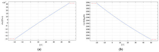
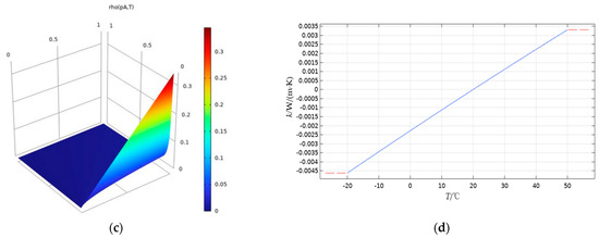
Figure 9.
Ambient domain parameters: (a) kinetic viscosity; (b) constant pressure heat capacity; (c) density; (d) thermal conductivity of air.
2.5. Analysis and Selection of the Ambient Temperatures
Figure 10 shows the all-year climate (annual weather averages) in Sydney. The averages performed are based on weather reports collected in the period 1985–2015 for Sydney Airport which is 9 km from Sydney. The temperatures from the months of December, January and February are the highest, with a temperature of 26–27 °C in the daytime and 18–20 °C in the evening; the temperatures from June to August are the lowest, with a temperature of about 17–19 °C in the daytime and 8–9 °C in the evening which are the worst-case scenarios. Furthermore, in the season of Autumn, from March to May, the temperatures decrease from 25 °C to 20 °C in the daytime, and 18–12 °C in the evening, respectively. In the season of Spring (from September to November) the temperatures increase from 21 to 24 °C in the daytime and 11 to 16 °C at night, respectively. Figure 11 gives the temperature changes in 2022 in Beijing, China. The highest temperatures occur in the season of summer from June to August which are around 32 °C in the daytime and 23 °C in the evening, respectively. In wintertime, the highest temperatures are 3 to 5 °C in the daytime and −7 to −9 °C in the evening, respectively.
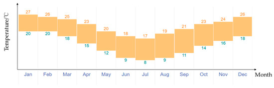
Figure 10.
The all-year climate (annual weather averages) in Sydney.
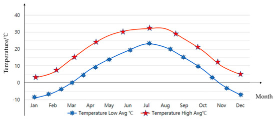
Figure 11.
The temperature change in 2022 in Beijing.
Based on the above temperatures, a series of ambient temperatures can be selected, which are −10 °C, 0 °C, 10 °C, 20 °C and 30 °C. In addition, high temperatures from 38 °C to 42 °C often occur in summer in Sydney. Therefore, 40 °C is also selected in this paper and an added temperature of 50 °C is the upper limit of the maximum ambient temperature.
3. Convection Thermal Coupling Modeling of Adjacent Devices
3.1. FEM Modeling
The calculation method of the thermal coupling effect for adjacent devices is complex. The calculation method of thermal conduction coupling in [11] is based on the principle of linear superposition: a power loss P is applied to one device (device I) and the temperature rise of the adjacent device (device II) is supposed to be caused by the thermal conduction coupling from device I. Then a power loss is applied to device II to observe the thermal coupling effect on device I. The conduction thermal coupling between device I and device II can be obtained by this method. However, it has limitations which are only applicable to linear relations [11,28]. The thermal coupling between power devices contains non-linear convection terms. Therefore, this causes errors if the superposition principle is still adopted [21]. Based on the above, FEM modeling is established in this paper to simulate the convection thermal coupling between adjacent power devices and to calculate the junction temperature at different ambient temperatures.
The boundary conditions are as follows [29,30,31]: (1) the packed side is considered to be insulated; (2) all thermal will flow from the copper substrate (case) and pins into the surrounding air; and (3) the thermal transferring mode is thermal conduction and natural convection. Probes are added at the key points to extract and compare the device temperature. The simulation runs for 1000 s until the device temperature reaches a stable state for a certain time.
This paper simplifies the structures of the power devices (MOSFET and diode) to better analyze the convective thermal coupling effect between adjacent devices. In addition, in order to obtain more accurate results and reduce simulation time, a multi-level grid meshing method is adopted where in the key layer (chip layer) finer mesh is given and in other layers such as substrate and PCB, a coarse mesh is used [32,33,34].
3.2. Convection Thermal Coupling Simulation and Junction Temperature Calculation
The power loss of the MOSFET is set to 5 W and the diode to 2 W. As the value of power loss for MOSFET is higher than that of the diode, the surrounding ambient temperature for MOSFET is also higher than that for the diode, and the color table shows the thermal distribution, as shown in Figure 12.
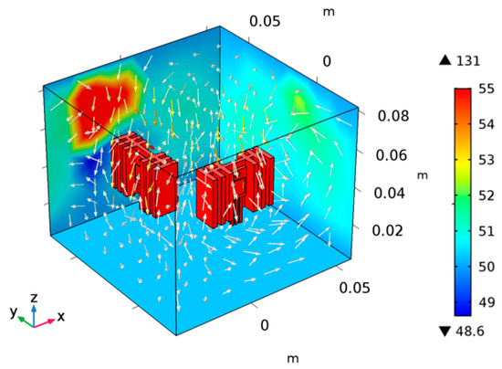
Figure 12.
The temperature distribution of convection thermal coupling.
Through the FEM analysis, the temperature distribution and iso-surface distribution of power devices under different ambient temperatures are obtained, as shown in Figure 13. In the figures below, the color tables show the difference in the distribution.
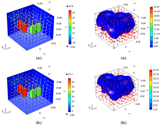
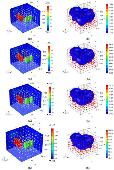
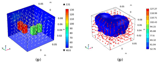
Figure 13.
Simulation analysis of convection thermal coupling. (a1,a2) are temperature distribution and iso-surface distribution when Ta = −10 °C; (b1,b2) are temperature distribution and iso-surface distribution when Ta = 0 °C; (c1,c2) are temperature distribution and iso-surface distribution when Ta = 10 °C; (d1,d2) are temperature distribution and iso-surface distribution at Ta = 20 °C; (e1,e2) are temperature distribution and iso-surface distribution at Ta = 30 °C; (f1,f2) are temperature distribution and iso-surface distribution at Ta = 40 °C; (g1,g2) are temperature distribution and iso-surface distribution at Ta = 50 °C.
In the simulation, the junction temperature of the devices can be directly detected by adding a virtual probe. The junction temperatures of the devices under different ambient temperatures can be obtained considering the convection thermal coupling between the power devices, as shown in Table 5.
Table 5.
The junction temperatures at different ambient temperatures.
4. The Relationships between the Junction and Ambient Temperatures
The steady-state junction temperatures of the power devices in Table 5 are used to fit the relationships between junction temperatures and ambient temperatures, and the relationships for MOSFET and diode are shown in Figure 14 and (6).
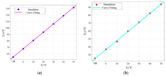
Figure 14.
The relationships between junction and ambient temperatures: (a) for MOSFET, (b) for diode.
The fitting coefficients of the relationships for MOSFET and diode are
As the ambient temperature will change with time changes, then when the ambient changes as a function of time [7], the relationships between the junction and ambient temperature can be expressed as
5. Modeling Verification
5.1. The Simulation Analysis under New Temperature Profile
To verify the correctness of the model and the relationship between device junction temperature and ambient temperature, a new finite element simulation model based on (5) and (2) and under the ambient temperature profile is established. The ambient temperature is 15 °C, 25 °C, 35 °C, 45 °C, respectively. The simulated temperature distribution and iso-surface distribution are shown in Figure 15.
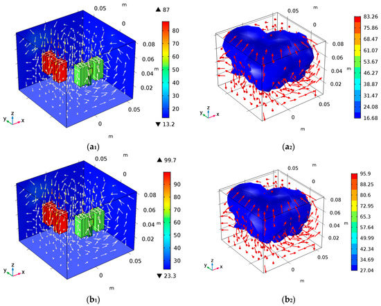
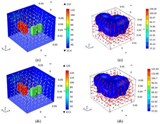
Figure 15.
The simulation analysis of convective heat coupling: (a1,a2) are the temperature distribution and iso-surface distribution at Ta = 15 °C, (b1,b2) are the temperature distribution and iso-surface distribution at Ta = 25 °C, (c1,c2) are the temperature distribution and iso-surface distribution at Ta = 35 °C, and (d1,d2) are the temperature distribution and iso-surface distribution at Ta = 45 °C.
5.2. Junction Temperature Calculation and Comparisons
The new junction temperatures can be obtained from FEM simulations in Figure 8 and the junctions at new ambient temperatures can be obtained through (6). The comparisons of the junction temperatures by simulation and calculation for MOSFET and diode are given in Table 6 and Table 7, respectively. By comparison, the maximum error of MOSFET is 0.08% and the maximum error of diode is 0.70%, which shows the feasibility and effectiveness of the proposed method.
Table 6.
The junction temperature comparisons of the calculation and simulation for the MOSFET.
Table 7.
The junction temperature comparisons of the calculation and simulation for the diode.
6. Conclusions
In view of the dependence of the convection thermal dissipation of the device itself and the convection thermal coupling effect between adjacent devices on the surrounding air region, a FEM simulation model of convection thermal coupling of adjacent devices at different ambient temperatures is established. By changing the environmental temperature profiles, the temperature distribution, iso-surface distribution, and junction temperature of the devices under different ambient temperatures are obtained, and the relationships between junction temperature and ambient temperature are deduced. The relationships are verified by the junction temperature of the device at the new ambient temperatures. The junction temperatures of the device at other ambient temperatures can be calculated by the proposed relationship. Moreover, a better understanding of the environmentally dependent temperatures will be desirable to assist in terms of power converter optimization.
Author Contributions
K.W. wrote the manuscript and performed the simulation. Thermal analysis was carried out by Y.Q. and P.S.; P.B. and Y.D. implemented the experimental platform; X.G. modified and improved the manuscript. All authors have read and agreed to the published version of the manuscript.
Funding
This work was funded partly by Tianjin Municipal Education Commission Scientific Research Program (No. 2022KJ120 and No. 2020KJ123), Tianjin Science and Technology Plan Project (No. 22YDTPJC00540) and Tianjin University of Technology and Education Scientific Research Launch Project, (No. KYQD202211).
Institutional Review Board Statement
Not applicable.
Informed Consent Statement
Not applicable.
Data Availability Statement
Not applicable.
Acknowledgments
The authors would like to thank the Ministry of Education’s “Chunhui Plan” cooperative scientific research projects.
Conflicts of Interest
The authors declare no conflict of interest.
References
- Gurpinar, E.; Ozpineci, B.; Chowdhury, S. Design, Analysis, Comparison and Experimental Validation of Insulated Metal Substrates for High Power Wide-Bandgap Power Modules. J. Electron. Packag. 2020, 142, 041107-1–041107-10. [Google Scholar] [CrossRef]
- Shahjalal, M.; Ahmed, M.; Lu, H.; Bailey, C.; Forsyth, A. An Analysis of the Thermal Interaction Between Components in Power Converter Applications. IEEE Trans. Power Electron. 2020, 35, 9082–9094. [Google Scholar] [CrossRef]
- Drofenik, U.; Cottet, D.; Müsing, A.; Meyer, J.-M.; Kolar, J.W. Modelling the thermal coupling between internal power semiconductor dies of a water-cooled 3300V/1200A HiPak IGBT module. In Proceedings of the Conference for Power Electronics, Intelligent Motion, Power Quality (PCIM’07), Nuremberg, Germany, 22–24 May 2007; pp. 22–24. [Google Scholar]
- Wei, K.; Cheng, T.; Siwakoti, D.L.Y.; Zhang, C. Multi-Variable Thermal Modeling of Power Devices Considering Mutual Coupling. Appl. Sci. 2019, 9, 3240. [Google Scholar] [CrossRef]
- Assila, H.; Essadiqi, E.; Faqir, M.; Meziane, M.; Ghanameh, F.; Ahzi, S. Numerical simulation of photovoltaic panel thermal condition under wind convection. In Proceedings of the 2016 International Renewable and Sustainable Energy Conference (IRSEC), Marrakech, Morocco, 14–17 November 2016; pp. 653–658. [Google Scholar]
- Sztykiel, M.; Fletcher, S.; Norman, P.; Galloway, S.; Burt, G.M. Electro-thermal analysis of power converter components in low-voltage DC microgrids for optimal protection system design. IEEE Trans. Smart Grid 2017, 9, 5843–5853. [Google Scholar] [CrossRef]
- Mathew, J.; Krishnan, S. A Review on Transient Thermal Management of Electronic Devices. J. Electron. Packag. 2022, 144, 010801–010821. [Google Scholar] [CrossRef]
- Kim, J.C.; Ren, Z.; Yuksel, A.; DeDe, E.M.; Bandaru, P.R.; Oh, D.; Lee, J. Recent Advances in Thermal Metamaterials and Their Future Applications for Electronics Packaging. J. Electron. Packag. 2021, 143, 010801-1–010801-15. [Google Scholar] [CrossRef]
- Lu, H.-L.; Lu, Y.-J.; Zhu, L.-H.; Lin, Y.; Guo, Z.-Q.; Liu, T.; Gao, Y.-L.; Chen, G.-L.; Chen, Z. Efficient measurement of thermal coupling effects on multichip light-emitting diodes. IEEE Trans. Power Electron. 2017, 32, 9280–9292. [Google Scholar] [CrossRef]
- Wei, K.; Lu, D.D.-C.; Zhang, C.; Siwakoti, Y.P.; Soon, J.L.; Yao, Q. Modeling and Analysis of Thermal Resistances and Thermal Coupling Between Power Devices. IEEE Trans. Electron Devices 2019, 66, 4302–4308. [Google Scholar] [CrossRef]
- Bahman, A.S.; Ma, K.; Blaabjerg, F. A novel 3D thermal impedance model for high power modules considering multi-layer thermal coupling and different heating/cooling conditions. In Proceedings of the 2015 IEEE Applied Power Electronics Conference and Exposition (APEC), Charlotte, NC, USA, 15–19 March 2015; pp. 1209–1215. [Google Scholar]
- Qian, C.; Gheitaghy, A.M.; Fan, J.J.; Tang, H.Y.; Sun, B.; Ye, H.Y.; Zhang, G.Q. Thermal management on IGBT power electronic devices and modules. IEEE Access 2018, 6, 12868–12884. [Google Scholar] [CrossRef]
- Wang, H.; Zhu, R.; Wang, H.; Liserre, M.; Blaabjerg, F. A Thermal Modeling Method Considering Ambient Temperature Dynamics. IEEE Trans. Power Electron. 2020, 35, 1307–1316. [Google Scholar] [CrossRef]
- Sintamarean, C.; Blaabjerg, F.; Wang, H. A novel electro-thermal model for wide bandgap semiconductor-based devices. In Proceedings of the 2013 15th European Conference on Power Electronics and Applications (EPE), Lille, France, 2–6 September 2013; pp. 1–10. [Google Scholar]
- Sheltami, K.; Refai-Ahmed, G.; Shwehdi, M. Thermal management of high-power transformer in different outdoor environment conditions. In Proceedings of the The Ninth Intersociety Conference on Thermal and Thermomechanical Phenomena in Electronic Systems (IEEE Cat. No. 04CH37543), Las Vegas, NV, USA, 14 June 2004; pp. 543–548. [Google Scholar]
- Jauregui, D. Estimating TJ of SO-8 Power MOSFETs; International Rectifier Semiconductor, Design Tip 99-2; International Rectifier: El Segundo, CA, USA, 2006. [Google Scholar]
- Tang, Y.; Ma, H. Dynamic electrothermal model of paralleled IGBT modules with unbalanced stray parameters. IEEE Trans. Power Electron. 2017, 32, 1385–1399. [Google Scholar] [CrossRef]
- Darwish, A.M.; Bayba, A.J.; Khorshid, A.; Rajaie, A.; Hung, H.A. Calculation of the nonlinear junction temperature for semiconductor devices using linear temperature values. IEEE Trans. Electron Devices 2012, 59, 2123–2128. [Google Scholar] [CrossRef]
- Chan, C.-J.; Hsu, F.-M.; Su, Y.-F.; Chiang, K.-N. Study on current and junction temperature stress aging effect for accelerated aging test of Light emitting diodes. In Proceedings of the 2016 International Conference on Electronics Packaging (ICEP), Hokkaido, Japan, 20–22 April 2016; pp. 62–65. [Google Scholar]
- Bruckner, T.; Bernet, S. Estimation and measurement of junction temperatures in a three-level voltage source converter. In Proceedings of the Fortieth IAS Annual Meeting. IEEE Conference Record of the 2005 Industry Applications Conference, Hong Kong, China, 2–6 October 2005; pp. 106–114. [Google Scholar]
- Shabany, Y. Heat Transfer: Thermal Management of Electronics; CRC Press: Boca Raton, FL, USA, 2009. [Google Scholar]
- Garimella, S.V.; Yeh, L.-T.; Persoons, T. Thermal management challenges in telecommunication systems and data centers. IEEE Trans. Compon. Packag. Manuf. Technol. 2012, 2, 1307–1316. [Google Scholar] [CrossRef]
- Ren, Y.; Xu, M.; Zhou, J.; Lee, F.C. Analytical loss model of power MOSFET. IEEE Trans. Power Electron. 2006, 21, 310–319. [Google Scholar]
- Reichl, J.; Ortiz-Rodriguez, J.M.; Hefner, A.; Lai, J.-S. 3-D thermal component model for electrothermal analysis of multichip power modules with experimental validation. IEEE Trans. Power Electron. 2015, 30, 3300–3308. [Google Scholar] [CrossRef]
- Niu, H.; Wang, H.; Ye, X.; Wang, S.; Blaabjerg, F. Converter-level FEM simulation for lifetime prediction of an LED driver with improved thermal modelling. Microelectron. Reliab. 2017, 76, 117–122. [Google Scholar] [CrossRef]
- Frey, P.J.; George, P.-L. Mesh Generation: Application to Finite Elements; Wiley-ISTE: Hoboken, NJ, USA, 2008. [Google Scholar]
- Lee, S.-Y.; Devarajan, M. Thermal analysis of multi-chip LED package with different position and ambient temperatures. In Proceedings of the 2011 2nd International Conference on Photonics, Kota Kinabalu, Malaysia, 17–19 October 2011; pp. 1–4. [Google Scholar]
- Bahman, A.S.; Ma, K.; Blaabjerg, F. A Lumped Thermal Model Including Thermal Coupling and Thermal Boundary Conditions for High-Power IGBT Modules. IEEE Trans. Power Electron. 2018, 33, 2518–2530. [Google Scholar] [CrossRef]
- Wang, Y.; Ao, J.; Liu, S.; Hao, Y. Thermal Modeling of the GaN-based Gunn Diode at Terahertz Frequencies. Appl. Sci. 2019, 9, 75. [Google Scholar] [CrossRef]
- Zhu, N. Analysis and Application of Electrical and Thermal Characteristics of Power Semiconductor Modules. Ph.D. Thesis, Zhejiang University, Hangzhou, China, 2018. [Google Scholar]
- Haifeng Sun, Y.W. Simulation of IGBT Thermal Model Based on Finite Element Method. Power Sci. Eng. 2019, 35, 15–22. [Google Scholar]
- Tan, L.; Liu, P.; She, C.; Xu, P.; Yan, L.; Quan, H. Heat Dissipation Characteristics of IGBT Module Based on Flow-Solid Coupling. Micromachines 2022, 13, 554. [Google Scholar] [CrossRef]
- Chen, Y.; Pan, X.; Deng, L. Study on the Localization of Defects in Typical Steel Butt Welds Considering the Effect of Residual Stress. Appl. Sci. 2023, 13, 2648. [Google Scholar] [CrossRef]
- Borghei, M.; Ghassemi, M. Characterization of Partial Discharge Activities in WBG Power Converters under Low-Pressure Condition. Energies 2021, 14, 5394. [Google Scholar] [CrossRef]


Disclaimer/Publisher’s Note: The statements, opinions and data contained in all publications are solely those of the individual author(s) and contributor(s) and not of MDPI and/or the editor(s). MDPI and/or the editor(s) disclaim responsibility for any injury to people or property resulting from any ideas, methods, instructions or products referred to in the content. |
© 2023 by the authors. Licensee MDPI, Basel, Switzerland. This article is an open access article distributed under the terms and conditions of the Creative Commons Attribution (CC BY) license (https://creativecommons.org/licenses/by/4.0/).