Abstract
A hybrid power modulator is presented for the radio frequency (RF) power amplifiers of 5th generation mobile communication technology (5G) new radio (NR) applications. A hybrid power modulator utilizing a two-level switching converter and a broadband and high-efficiency linear amplifier is presented. A further improvement in the efficiency of the circuit is achieved by using an optimized supply voltage of the two-level switching converters of 4.5 V. In this way, the overall efficiency is improved by more than 5% compared to using a 5 V supply voltage. The linear amplifier consists of four stages. In order to improve bandwidth and circuit stability, a compensation circuit is added to the linear amplifier that eliminates the poles of the main amplifier by introducing additional zeros, indirectly pushing the pole distribution out of the bandwidth. Using this approach, the linear amplifier achieves a 3-dB bandwidth of 180 MHz and an efficiency of 51%. The hybrid power modulator achieves a maximum output power of 2.4 W and an efficiency of 86% when tracking a 100 MHz 5G-NR signal under a 4 Ω load in a 180 nm CMOS package.
1. Introduction
In communication systems, the power amplifier is the most critical component but also the most energy-consuming component. Therefore, the performance of the designed power amplifier directly affects the performance of the entire system [1,2,3,4]. Up to now, envelope tracking technology (ET) [4,5,6,7] has been the main technology used to improve the efficiency of power amplifiers. The basic architecture of ET technology is shown in Figure 1. The baseband signal is up-converted after delay correction as the input signal of the power amplifier. The baseband signal of the other channel is used as the input signal of the power modulator after envelope detection and envelope processing. The power supply modulator is the key to ET technology, and its output voltage should track the input signal of the envelope well. The power supply modulator has high conversion efficiency to improve the efficiency of the entire power amplifier system. In order to enhance the efficiency and bandwidth of power supply modulators, various methods have been proposed. Power supply modulators come in three main forms, switching converters [8,9,10], linear amplifiers [11,12,13,14,15], and hybrid power modulators [16,17,18,19,20,21,22]. When switching converters process relatively wide information, the frequency of the switching transistor of the switching converter is required to be 5–6 times that of the processing envelope signals. This increases losses and reduces efficiency. Wide band-gap device technology has been proposed to improve the efficiency of switching converters [23,24,25]. Multi-phase structure and multi-level structure have also been achieved [26,27]. For linear amplifiers, it is easy to introduce losses and decrease the efficiency with the increase of peak-to-average ratio. The hybrid power supply modulator mainly includes switching converters, linear amplifiers, and controllers. This structure makes switching converters process information to improve efficiency, while the linear amplifiers process information to improve linearity. In order to improve efficiency, the controller is a tradeoff between efficiency and bandwidth. The hybrid power supply modulator has more advantages than other structures. The characteristics of linear amplifiers in hybrid power supply modulators are wide band, small output impedance, high gain, and large swing [28,29,30]. The common control methods are PWM control [31] and hysteretic control [32]. Switching converter structures are multi-phase [31,33] or multi-level [34]. Controlling multilevel switching converters is a challenge. More levels need more complicated circuits to be designed [35]. In [16], the bandwidth of a dual-mode hybrid power supply modulator, which consists of a hybrid power modulator and an average power tracking, is limited to 40 MHz. In [31], a hybrid power modulator composed of a class-AB linear amplifier and a two-phase switching converter is proposed, but it only tracks 4 MHz rectified sine waves. In [36], an ac-coupling of the outputs of the linear amplifier is proposed to improve the efficiency of a hybrid power supply modulator; however, the output method requires a large coupling capacitance, resulting in increased area. In [37], tracking and controlling the current of a linear amplifier optimizes the current distribution which results in limiting bandwidth. It can be seen from the studies cited above, although different structures have been tried in attempts to implement power supply modulators, it is challenging to design a highly efficient and wide bandwidth hybrid power supply modulator.
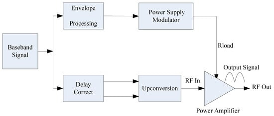
Figure 1.
Basic block diagram of envelope tracking.
In communication systems based on envelope tracking technology, a mismatch between the envelope and the phase reduces Error Vector Magnitude (EVM). Thus, it is also important to increase the bandwidth of a hybrid power modulator. In this paper, an efficiency-86% hybrid power modulator for 5G New Radio (NR) is proposed. A current-mirror amplifier with current reuse is introduced, which is followed by a class-AB buffer. Compared to other linear amplifiers, this method achieves a wide bandwidth and high efficiency by introducing extra zeros. It optimizes the voltage value to improve its efficiency without multi-phase or multi-level switching converters. In the second section, the technology and methods of realizing hybrid power supply modulators are discussed. In the third, the results are analyzed. In the final section, the conclusions are reported.
2. Technology and Methods
The hybrid power supply modulator is mainly divided into three parts, a switching converter, a linear amplifier, and a hysteresis comparator, as shown in Figure 2. The linear amplifier realizes the linear amplification of the envelope signal, and mainly consists of operational amplifiers and push-pull circuits. The linear amplifier mainly provides voltage and a small current to the power modulator, as shown in Figure 3. The output stage adopts a class-AB structure. The class-AB structure has three advantages: first, the power transistor in the structure is in a micro-conduction state, and the power consumption is small in this state; second, the output of the first stage amplifier can track the input signal better; and, third, the bias mode of the class-AB type allows the transistor to have a larger current output capability [38].
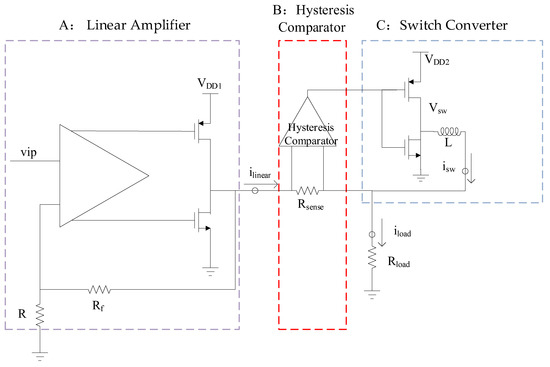
Figure 2.
Typical architecture of a hybrid power supply modulator.
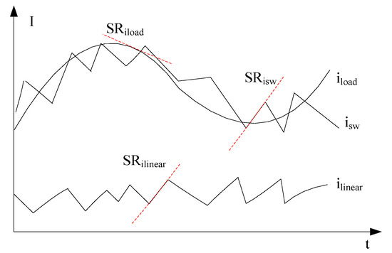
Figure 3.
The key waveform of current through a hybrid power modulator.
The switching converter is directly controlled by the hysteresis comparator. When the envelope signal is in the low-frequency band, the switching converter is turned on and off to provide current to the power supply modulator. The linear amplifier mainly deals with high-frequency signals. In Figure 2, module A is the linear amplifier, module B is the hysteresis comparator, and module C is the switching converter. , where is the output current of the linear amplifier, is the current of switching converter, and is the current of the whole circuit, as shown in Figure 3.
When the input signal (vip) frequency is low, the slew rate of the switching converter SRisw is much higher than the slew rate of SRiload [39], and the switching converter can track the input signal. The linear amplifier cancels the ripple from the switching converter. When the input signal (vip) is high frequency, the slew rate of the switching converter SRisw is lower than the slew rate of SRiload; when this happens, the switching converter cannot track the input signal, and the linear amplifiers provide a high slew rate of SRilinear to track the high-frequency signal assisting the switching converter.
2.1. The Structure of the Linear Amplifier
In the process of designing a hybrid power modulator, the output resistance of the linear amplifier should be very low to drive the following circuits. Its high voltage gain ensures tracking accuracy. The wide bandwidth of the linear amplifier is required for quick response. The unit gain bandwidth requires a large loss current while increasing the linear stage bandwidth, and a large current consumption. How to meet the requirements of the linear amplifier is also a key point.
The current-mirror amplifier with current reuse is based on a current mirror operational trans-conductance amplifier (OTA) as shown in Figure 4. An additional control circuit is added to increase the output current, as shown in Figure 5. In static conditions, the static currents of M3 and M4 are shunted by adding two transistors M12 and M13, which reduces the output current and indirectly increases the output impedance. The magnitudes of the current flowing through M12 and M13 are controlled by the detection input differential voltage of M10, M11, M14, and M15. The output impedance, gain, and slew rate of a current-mirror amplifier with current reuse are better than those for a current-mirror OTA under the same working conditions. Therefore, this structure of a current-mirror amplifier with current reuse is more suitable for the design of linear amplifiers.
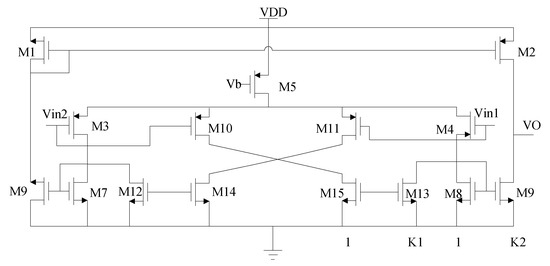
Figure 4.
Current-mirror amplifier with current reuse.
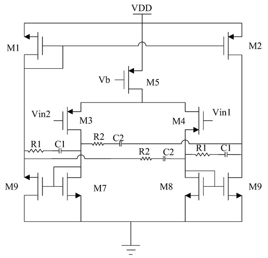
Figure 5.
Schematic diagram of phase enhancement method circuit.
The stability of a linear amplifier depends primarily on the distribution of poles and zeros. The phase margin (PM) is referred to as a unique parameter for a closed-loop system. A good phase margin can make the system more stable. How to ensure that the linear amplifier has suitable stability is also a key issue in the study of power supply modulator chips. One approach to accomplishing this is to introduce a compensation circuit to move poles into the system to stabilize the whole system. Utilizing traditional Miller compensation [13], the main idea is to reduce the bandwidth in exchange for the improvement of the phase margin. In this paper, a phase enhancement method in the main amplifier is used to improve the stability of the linear amplifier [14,15].
In this paper, two zeros are introduced by using negative feedback and positive feedback resistor-capacitor links. Two zeros are used to cancel the original two poles in the main amplifier, thereby indirectly pushing the frequency of the secondary poles out of the bandwidth range as shown in Figure 6. This increases the bandwidth and phase margin. As the frequency of the zero is entirely determined by the passive component values, zero-pole cancelation can be easily achieved [15]. The second pole () can be eliminated by adjusting the first zero () with the sum of and . The second zero () can then be tuned to the frequency of the third pole () [15].
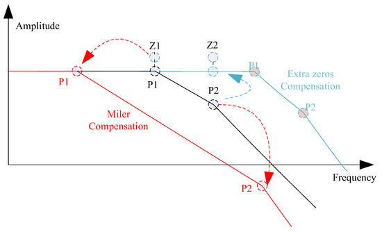
Figure 6.
Frequency response for Miller compensation and the proposed compensation.
This paper assumes that C1 = C2 = C [16].
In order to make full use of the power supply voltage and reduce power consumption, the output stage needs to provide a large current and a small quiescent current. The output stage adopts class-AB amplifier architecture after compromise M53 and M54 are used to form a floating voltage source to fix the gate voltage to make the output stage work in class-AB mode. As for the compensation of the secondary amplifier and the class-AB amplifier, since the pole of the main amplifier is offset by the introduced zero point, the main pole of the secondary amplifier becomes the main pole of the whole circuit. As the transistor of the class-AB amplifier is large, it can be used as compensatory capacitance. At the same time, because the output load resistance of the class-AB amplifier is small, and the drain resistance of the power amplifier is only about 4 ohms, the high-frequency pole will move to high frequency. Therefore, it is not necessary to compensate again. In summary, the final design of the main part of the linear amplifier is shown in Figure 7.
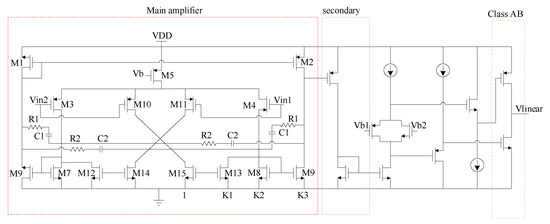
Figure 7.
Circuit diagram of the linear amplifier.
2.2. The Switching Converter and the Hysteresis Comparator
The hysteresis comparator plays an essential role in achieving high efficiency as shown in Figure 8. Hysteresis control has the advantages of fast response speed, no need for an additional stable compensation circuit, simple implementation, and a small area. By detecting the output current between the linear amplifier and the switching converter, the linear amplifier is indirectly controlled by the hysteresis comparator to generate additional output current to offset the amplification error current that is generated by the switching converter.
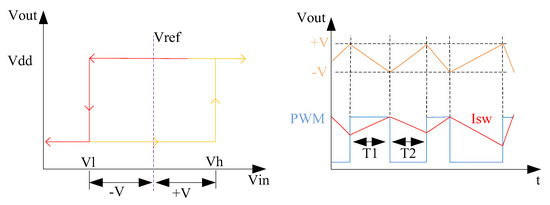
Figure 8.
The control logic of the hysteresis comparator.
When the detection current is too small, the switching frequency will become higher, which results in a larger switching loss. When the detection current is too large, the switching frequency will become smaller, which results in more current being provided by the linear stage and worse linearity. Therefore, the circuit parameters (Rsense, L, h) need to be optimized to achieve a circuit design of high efficiency and high linearity. is the current sensing resistor, L is a filter inductance, h is the hysteresis width, and, as shown in Equations (6)–(11), the switching converter is related to Rsense, L, h, .
The hysteresis comparator includes an input stage amplifier, pre-judgment, and an output stage. The prediction gain is improved by the cross-connection of the positive feedback transistors, M40, and M41. Assuming that is much greater than , M39 and M41 are turned on and M40 and M42 are turned off, as shown in Figure 9. The width-to-length ratio of M39 and M42 is ; while the width-to-length ratio of M40 and M41 is . The current of M41 is the mirror of the current of M39. As shown in Equation (13), wherein gm is the trans-conductance of the transistor M34, when is not equal to , the comparator functions as a hysteresis comparator. The upper corner voltage of the comparator is , the lower corner voltage is is the current of M36 [20].
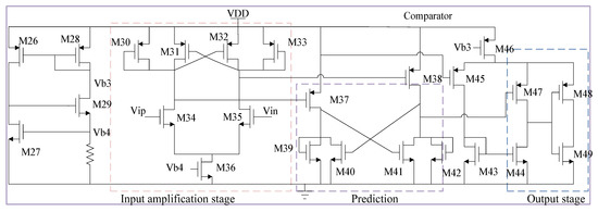
Figure 9.
Circuit diagram of the hysteresis comparator.
The efficiency of the power supply modulator also depends on the application. For broadband applications, the hysteresis width should be minimized—although this is the opposite for narrowband applications in some cases because a small hysteresis bandwidth will cause a higher switching frequency and more losses [39]. How to improve the efficiency of power supply modulators with different input signals has become a focus of research. In order to solve this problem, some researchers have changed the controllers or the number of switching converters. In this paper, optimizing the supply voltage of the switching converters improves efficiency. Optimizing the supply voltage in steps of ΔV (V1 − Vn) indirectly increases the switching frequency [15], as shown in Figure 10. In Figure 10, the reference voltage VDD2min is defined as the average value of 2*vip, ti (i = 1, 2,…) is the time period of i, and Wt (t = 1, 2,…) is a series of subsections of the output of the linear amplifier.

Figure 10.
Procedure and simplified circuit model of a hybrid power supply modulator.
3. Results and Discussion
All circuits as shown in Figure 11 are fabricated in a 0.18 μm Complementary Metal Oxide Semiconductor (CMOS) technology package. Circuits are simulated by Cadence software.
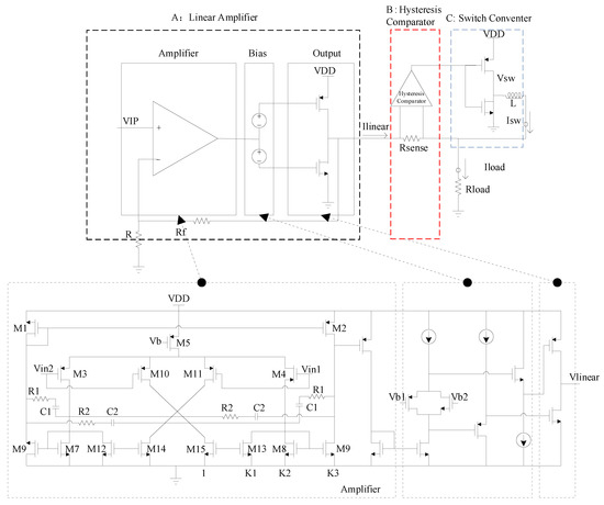
Figure 11.
The basic architecture of the hybrid power supply modulator.
The simulation of the closed-loop performance of the linear amplifier is shown in Figure 12. Figure 12a shows the case of Miller compensation of the closed-loop performance. It shows a twice gain frequency of 32 MHz and a phase margin of 60°; thus, the GBW is about 64 MHz. Figure 12b shows the case for compensation of the closed-loop performance using positive feedback to introduce extra zeros. This shows a twice gain frequency of 117 MHz and a phase margin of 42°; thus, the GBW is about 234 MHz. At 100 MHz, the phase margin is about 60°. Meanwhile, the 3-dB bandwidth of the linear amplifier simulated is about 180 MHz, as shown in Figure 13. Compared to the Miller compensation approach, this method is better.
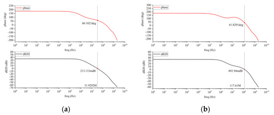
Figure 12.
(a) Miller compensation, and (b) compensation by introducing extra zeros.
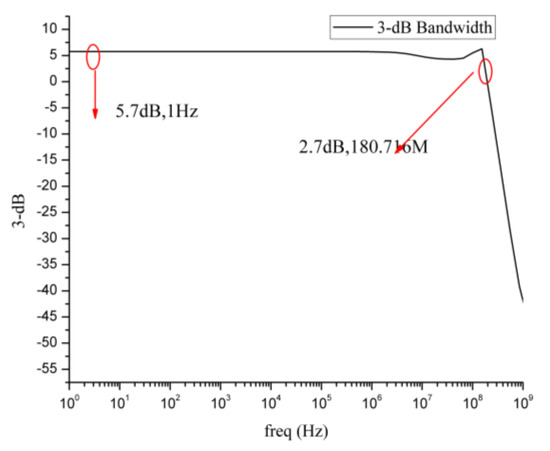
Figure 13.
The 3-dB bandwidth of the linear amplifier.
The instantaneous simulation of the hybrid power modulator is carried out, in which the input signal is a 5G-NR signal with a bandwidth of 100 MHz. The results show that the average power efficiency of the linear amplifier is 51%.
Transient simulation of the hybrid power modulator is also carried out, in which the input signal is vip, the output current is iout, the output voltage of switching converters is Vsw, and the output current through the inductor L is isw, Rload = 7 Ω, as shown in Figure 14. The different VDD2 and different Rload on the output efficiency are shown in Figure 15.
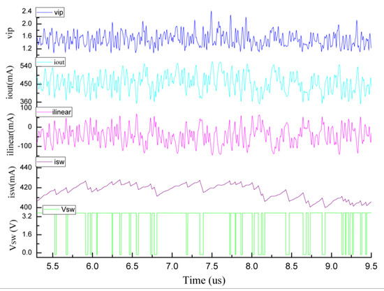
Figure 14.
The current of the hybrid power modulator.
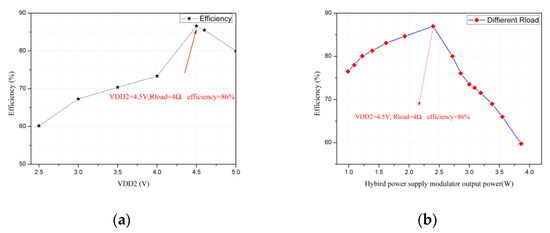
Figure 15.
Influence of (a) different VDD2 and (b) different Rload on the output efficiency.
A comparison of the performance of the hybrid power modulator proposed in this work and modulators reported in the literature is shown in Table 1. Hybrid power modulators consist principally of linear amplifiers, switching converters, and controllers. Optimizing the performance of each module reduces losses and improves bandwidth. To achieve this, changing the level number of the switching converter is a research trend [40]. The method by which the controller controls the switching converters by changing the way that voltage is detected [39,41,42,43,44] is also the focus of research to improve efficiency.

Table 1.
Comparison of power supply modulators.
4. Conclusions
In this paper, the linear amplifier compensation circuit of a hybrid power modulator is improved by introducing extra zeros. Compared with an approach based on Miller compensation, this method results in an improved gain bandwidth product. A further improvement in efficiency is achieved by using an optimized supply voltage of the two-level switching converter of 4.5 V. The maximum efficiency of the hybrid power supply modulator is 86%, and the output power is 2.4 W in a 0.18-m CMOS package.
Author Contributions
X.C. and X.Q. conceived and designed the experiments; X.C. and Y.L. performed the experiments; X.L. and T.W. analyzed the data; X.C. wrote the paper. All authors have read and agreed to the published version of the manuscript.
Funding
This research is supported by the National Natural Science Foundation of China under grant No. 61971414 and Henan Province Key R&D and Promotion Project (Science and Technology Research) No. 212102210027 and Zhengzhou Zhongke Institute of Integrated Circuit and System Application Research Dean Fund No. ZK2005BN003.
Institutional Review Board Statement
Not applicable.
Informed Consent Statement
Not applicable.
Data Availability Statement
The data can be obtained from the authors on request.
Conflicts of Interest
The authors declare no conflict of interest.
References
- Gupta, A.; Jha, E.R.K. A survey of 5G network: Architecture and emerging technologies. IEEE Access 2015, 3, 1206–1232. [Google Scholar] [CrossRef]
- Kawanishi, T.; Kanno, A.; Freire, H.S.C. Wired and wireless links to bridge networks: Seamlessly connecting radio and optical technologies for 5G networks. IEEE Microw. Mag. 2018, 19, 102–111. [Google Scholar] [CrossRef]
- Chih-Lin, I.; Han, S.; Xu, Z.; Wang, S.; Sun, Q.; Chen, Y. New paradigm of 5G wireless Internet. IEEE J. Sel. Areas Commun. 2016, 34, 474–482. [Google Scholar]
- Tsai, W.-T.; Peng, Z.-A.; Liou, C.-Y.; Mao, S.-G. Linearity and Noise Improvements of Driver-Stage Envelope-Injection Power Amplifier with Amplitude and Phase Shaping Functions for 5G New Radio Application. IEEE Access 2019, 7, 112384–112396. [Google Scholar] [CrossRef]
- Kim, J.; Son, J.; Jee, S.; Kim, S.; Kim, B. Optimization of Envelope Tracking Power Amplifier for Base-Station Applications. IEEE Trans. Microw. Theory Tech. 2013, 61, 1620–1627. [Google Scholar] [CrossRef]
- Mahmoudidaryan, P.; Mandal, D.; Bakkaloglu, B.; Kiae, S. 27.5 A 91%-Efficiency Envelope-Tracking Modulator Using Hysteresis-Controlled Three-Level Switching Regulator and Slew-Rate-Enhanced Linear Amplifier for LTE-80MHz Applications. In Proceedings of the 2019 IEEE International Solid-State Circuits Conference—(ISSCC), San Francisco, CA, USA, 17–21 February 2019. [Google Scholar]
- Renaud, L.; Baylon, J.; Gopal, S.; Hoque, M.A.; Heo, D. Analysis of Systematic Losses in Hybrid Envelope Tracking Modulators. IEEE Trans. Circuits Syst. I Regul. Pap. 2019, 66, 1319–1330. [Google Scholar] [CrossRef]
- Wolff, N.; Heinrich, W.; Bengtsson, O. 100-MHz GaN-HEMT Class-G Supply Modulator for High-Power Envelope-Tracking Applications. IEEE Trans. Microw. Theory Tech. 2016, 65, 872–880. [Google Scholar] [CrossRef]
- Rodriguez, M.; Zhang, Y.; Maksimovic, D. High frequency PWM buck converters using GaN-on-SiCHEMTs. IEEE Trans. Power Electron. 2014, 29, 2462–2473. [Google Scholar] [CrossRef]
- Sepahvand, A.; Zhang, Y.; Maksimović, D. High efficiency 20–400 MHz PWM converters using air-core inductors and monolithic power stages in a normally-off GaN process. In Proceedings of the 2016 IEEE Applied Power Electronics Conference and Exposition (APEC), Long Beach, CA, USA, 20–24 March 2016; pp. 580–586. [Google Scholar]
- Attili, I.B.; Mahmoud, S.A. Survey on Single Stage Amplifiers for Column Drivers in Active Matrix LCD Panels Leading to a Highly Linear Rail-to-Rail Robust Amplifier. IEEE Access 2019, 7, 166629–166647. [Google Scholar] [CrossRef]
- Yan, Z.; Mak, P.-I.; Law, M.-K.; Martins, R.P.; Maloberti, F. Nested-Current-Mirror Rail-to-Rail-Output Single-Stage Amplifier with Enhancements of DC Gain, GBW and Slew Rate. IEEE J. Solid-State Circuits 2015, 50, 2353–2366. [Google Scholar] [CrossRef]
- Sheeparamatti, A.; Bhat, M.V.; Srivatsa, M.P.; Nithin, M. Design of 3.3 V rail to rail operational amplifier for high resolution ADC driver amplifier. In Proceedings of the 2017 International Conference on Innovative Mechanisms for Industry Applications (ICIMIA), Bengaluru, India, 21–23 February 2017. [Google Scholar]
- Abdulaziz, M.; Nejdel, A.; Törmänen, M.; Sjöland, H. A 3.4 mW 65nm CMOS 5th order programmable active-RC channel select filter for LTE receivers. In Proceedings of the 2013 IEEE Radio Frequency Integrated Circuits Symposium (RFIC), Seattle, WA, USA, 2–4 June 2013. [Google Scholar]
- Abdulaziz, M.; Törmänen, M.; Sjöland, H. A Compensation Technique for Two-Stage Differential OTAs. IEEE Trans. Circuits Syst. II Express Briefs 2014, 61, 594–598. [Google Scholar] [CrossRef]
- Liu, S. Research and Implementation of Doherty RF Power Amplifier Based on Broadband Envelope Tracking Technology. Master’s thesis, Beijing University of Posts and Telecommunications, Beijing, China, 2015. [Google Scholar]
- Cao, T.; Liu, Y.; Yang, C.; Zhou, J. Circuits Optimization and System Linearization for High Efficiency and Wideband Envelope Tracking Architecture. J. Electron. Inf. 2020, 42, 787–794. [Google Scholar]
- Leng, W. Envelope-Tracking Supply Modulator with Trellis Search-Based Switching and 160 MHz Capability. In Proceedings of the 2021 IEEE Custom Integrated Circuits Conference (CICC), Austin, TX, USA, 25–30 April 2021. [Google Scholar]
- Lin, Y.-C.; Chen, Y.-J.E. A CMOS Envelope Tracking Supply Converter for RF Power Amplifiers of 5G NR Mobile Terminals. IEEE Trans. Power Electron. 2021, 36, 6814–6823. [Google Scholar] [CrossRef]
- Xiong, Y. High-Efficiency CMOS Envelope Amplifier Chip Design. Master’s thesis, University of Electronic Science and Technology, Chengdu, China, 2016. [Google Scholar]
- Wang, Y.; Ruan, X.; Jin, Q.; Xi, H.; Xiong, X.; Leng, Y.; Li, Y. Elimination of the Interaction of the Converters in Switch-Linear Hybrid Envelope Tracking Power Supplies. IEEE Trans. Power Electron. 2019, 35, 2053–2066. [Google Scholar] [CrossRef]
- Wang, Y.; Ruan, X.; Leng, Y.; Li, Y. Hysteresis Current Control for Multilevel Converter in Parallel-Form Switch-Linear Hybrid Envelope Tracking Power Supply. IEEE Trans. Power Electron. 2018, 34, 1950–1959. [Google Scholar] [CrossRef]
- Zhang, Y.; Strydom, J.; de Rooij, M.; Maksimović, D. Envelope tracking GaN power supply for 4G cell phone base stations. In Proceedings of the 2016 IEEE Applied Power Electronics Conference and Exposition (APEC), Long Beach, CA, USA, 20–24 March 2016. [Google Scholar]
- Sagneri, A.; Anderson, D.; Perreault, D. Optimization of integrated transistors for very high frequency dc-dc converters. IEEE Trans. Power Electron. 2013, 28, 3614–3626. [Google Scholar] [CrossRef]
- Zhang, Y.; Rodriguez, M.; Maksimovic, D. High frequency synchronous buck converter using GaN-on-SiC HEMTs. In Proceedings of the 2013 IEEE Energy Conversion Congress and Exposition, Denver, CO, USA, 15–19 September 2013. [Google Scholar]
- Zhang, Y.; Rodriguez, M.; Maksimovic, D. Output filter design in high-efficiency wide-bandwidth multi-phase buck envelope amplifiers. In Proceedings of the 2015 IEEE Applied Power Electronics Conference and Exposition (APEC), Charlotte, NC, USA, 15–19 March 2015. [Google Scholar]
- Sebastian, J.; Fernandez-Miaja, P.; Ortega-Gonzalez, F.; Patino, M.; Rodriguez, M. Design of a two-phase buck converter with fourth-order output filter for envelope amplifiers of limited bandwidth. IEEE Trans. Power Electron. 2014, 29, 5933–5948. [Google Scholar] [CrossRef]
- Liu, X.; Zhang, H.; Mok, P.K.T.; Luong, H.C. A Multi-Loop-Controlled AC-Coupling Supply Modulator with a Mode-Switching CMOS PA in an EER System With Envelope Shaping. IEEE J. Solid-State Circuits 2019, 54, 1553–1563. [Google Scholar] [CrossRef]
- Ziraksaz, F.; Nabavi, A. Design of a Linear Class AB Amplifier with 55dB Gain, 890MHz Bandwidth and Low Output Impedance for Envelope Tracking Supply Modulator. In Proceedings of the 2019 27th Iranian Conference on Electrical Engineering (ICEE), Yazd, Iran, 30 April–2 May 2019; pp. 253–257. [Google Scholar]
- Mahmoudidaryan, P.; Mandal, D.; Bakkaloglu, B.; Kiaei, S. Wideband Hybrid Envelope Tracking Modulator With Hysteretic-Controlled Three-Level Switching Converter and Slew-Rate Enhanced Linear Amplifier. IEEE J. Solid-State Circuits 2019, 54, 3336–3347. [Google Scholar] [CrossRef]
- Wu, P.Y.; Mok, P.K.T. A two-phase switching hybrid supply modulator for RF power amplifiers with 9% efficiency improvement. IEEE J. Solid-State Circuits 2010, 45, 2543–2556. [Google Scholar] [CrossRef]
- Hassan, M.; Larson, L.E.; Leung, V.W.; Asbeck, P.M. A combined series-parallel hybrid envelope amplifier for envelope tracking mobile terminal RF power amplifier applications. IEEE J. Solid-State Circuits 2012, 47, 1185–1198. [Google Scholar] [CrossRef]
- Sankman, J.; Song, M.K.; Ma, D. Switching-converter-only multiphase envelope modulator with slew rate enhancer for LTE power amplifier applications. IEEE Trans. Power Electron. 2016, 31, 817–826. [Google Scholar] [CrossRef]
- Amò, P.; Thomas, M.; Molata, V.; Jeřábek, T. Envelope modulator for multimode transmitters with AC-coupled multilevel regulators. In Proceedings of the 2014 IEEE International Solid-State Circuits Conference Digest of Technical Papers (ISSCC), San Francisco, CA, USA, 9–13 February 2014. [Google Scholar]
- Qu, L.; Li, S.; Yu, K.; Zhang, G. Three level envelope modulator for envelope tracking power amplifier. Appl. Electron. Technol. 2019, 45, 70–73+82. [Google Scholar]
- Riehl, P.; Fowers, P.; Hong, H.-P.; Ashburn, M. An AC-coupled hybrid envelope modulator for HSUPA transmitters with 80% modulator efficiency. In Proceedings of the 2013 IEEE International Solid-State Circuits Conference Digest of Technical Papers, San Francisco, CA, USA, 17–21 February 2013. [Google Scholar]
- Tan, M.; Ki, W.-H. An efficiency-enhanced hybrid supply modulator with single-capacitor current-integration control. IEEE J. Solid-State Circuits 2016, 51, 533–542. [Google Scholar]
- Pan, X.; Liu, H.; Zhang, H.; Xu, P.; Hong, Z. A dual-mode hybrid envelope tracking power modulator for RFPA. J. Fudan Univ. 2019, 58, 425–432. [Google Scholar]
- He, H.; Ge, T.; Kang, Y.; Guo, L.; Chang, J.S. A 40 MHz Bandwidth, 91% Peak Efficiency, 2.5 W Output Power Supply Modulator with Dual-Mode Sigma–Delta Control and Adaptive Biasing Amplifier for Multistandard Communications. IEEE Trans. Power Electron. 2020, 35, 9430–9442. [Google Scholar] [CrossRef]
- Hassan, M.; Asbeck, P.M.; Larson, L.E. A CMOS dual-switching power-supply modulator with 8% efficiency improvement for 20MHz LTE Envelope Tracking RF power amplifiers. In Proceedings of the 2013 IEEE International Solid-State Circuits Conference Digest of Technical Papers, San Francisco, CA, USA, 17–21 February 2013. [Google Scholar]
- Chen, Z.; Xia, Q.; Dong, L.; Fan, S.; Han, K.; Guo, Z.; Xue, Z.; Geng, L. An Open Loop Digitally Controlled Hybrid Supply Modulator Achieving High Efficiency for Envelope Tracking with Baseband up to 200-MHz. IEEE Trans. Circuits Syst. I Regul. Pap. 2020, 67, 4142–4153. [Google Scholar] [CrossRef]
- Kim, J.; Kim, D.; Cho, Y.; Kang, D.; Park, B.; Moon, K.; Koo, S.; Kim, B. Highly Efficient RF Transmitter Over Broad Average Power Range Using Multilevel Envelope-Tracking Power Amplifier. IEEE Trans. Circuits Syst. I Regul. Pap. 2015, 62, 1648–1657. [Google Scholar] [CrossRef]
- Jing, Y.; Bakkaloglu, B. A High Slew-Rate Adaptive Biasing Hybrid Envelope Tracking Supply Modulator for LTE Applications. IEEE Trans. Microw. Theory Tech. 2017, 65, 3245–3256. [Google Scholar] [CrossRef]
- Lin, W.; Lin, Z.; Liu, C.; Chen, K.; Lin, Y.; Lin, J.; Tsai, T. A 20 MHz Low Dropout Controlled Current Sensor for Constant On-Time Based Envelop Tacking Supply Modulator for Radio Frequency Power Amplifier. In Proceedings of the 2018 IEEE International Symposium on Circuits and Systems (ISCAS), Florence, Italy, 27–30 May 2018; pp. 1–4. [Google Scholar]
Publisher’s Note: MDPI stays neutral with regard to jurisdictional claims in published maps and institutional affiliations. |
© 2022 by the authors. Licensee MDPI, Basel, Switzerland. This article is an open access article distributed under the terms and conditions of the Creative Commons Attribution (CC BY) license (https://creativecommons.org/licenses/by/4.0/).