Abstract
The development and approbation of a superconducting local oscillator based on a long Josephson junction made it possible to create a fully superconducting integrated receiver in sub-terahertz frequency range, which was successfully tested both on board a high-altitude balloon and in the laboratory. In order to expand the frequency range of a superconducting integrated local oscillator, it is necessary to ensure the continuous tuning of its frequency at an arbitrary bias current, including a so-called resonant mode regime. The resonant mode regime takes place for high-quality tunnel junctions with low leakage; in this regime, stable generation is possible only at Fiske steps, the distance in frequency between which is tens of GHz. A method for suppressing resonances has been proposed and implemented; this method is based on the introduction of normal metal layers into the region near the long Josephson junction. Modeling of the propagation of electromagnetic waves in the proposed integrated structure was carried out; experimental samples were fabricated, and their comprehensive study was performed. The complete suppression of resonances and the possibility of the continuous tuning of the frequency of a superconducting local oscillator in the range of 200–700 GHz have been demonstrated. The linewidth of the FFO radiation does not exceed 15 MHz over the entire frequency range, which makes it possible to implement the phase locked loop mode in an integrated receiver intended for spectral studies.
1. Introduction
Superconducting devices have unique characteristics that are unattainable for conventional semiconductor electronics. The ability of superconducting nanostructures to operate at very high frequencies, along with their extremely strong non-linear response, makes them ideal building blocks for state-of-the-art systems designed to detect and to generate terahertz radiation. The development of supersensitive terahertz (THz) receivers and oscillators is currently one of the most intensively and successfully developing areas of superconducting electronics [1,2,3,4,5,6,7,8,9,10,11]. Superconducting elements have an extremely low intrinsic noise due to their cryogenic operating temperature and quantum nature of mixing [12,13,14]; this, in addition to the listed advantages, enables the development of terahertz receivers with unique parameters that are unreachable for devices based on other physical principles. In the frequency range from 100 GHz to 1.4 THz, the most sensitive receiving elements are superconductor-insulator-superconductor (SIS) junctions [14,15,16]. The development of superconducting electronics made it possible to create a superconducting integrated receiver (SIR) [17,18], which combines all receiver components in one chip: a planar antenna, a SIS mixer, a superconducting local oscillator, and an additional harmonic SIS mixer for phase locking of the local oscillator. The high sensitivity and spectral resolution of the SIR were demonstrated while probing the atmospheric limb aboard a high-altitude balloon [19], and in the laboratory for detailed spectral measurements of terahertz radiation emitted by the Bi2Sr2CaCu2O8 mesa structure, formed by thousands of Josephson junctions [20]. A number of other experiments dedicated to studying the spectra of sub-THz signals were also investigated [21,22,23].
The superconducting local oscillator, also known as FFO [24,25,26,27,28,29], is based on a long Josephson junction (LJJ), whose length L is much greater than its width W and the Josephson penetration depth λJ = (Φ0/(2π µ0 jc l))1/2; where Φ0 = h/2e, jc is critical current density of the junction, l = d + λL1 + λL2 is magnetic thickness of the tunnel junction, d is the barrier thickness, λL1,2-magnetic field (London) penetration depth of the superconducting electrodes. In such a long junction, a unidirectional motion of Josephson vortices-fluxons, containing a single magnetic flux quantum Φ0 arises due to joint action of the applied magnetic field and the transport current, called the bias current Ib. When the vortex reaches the end of the junction, electromagnetic radiation is emitted. In accordance with the Josephson relation, the junction biased at voltage V generates electromagnetic oscillations with frequency f = (2π/Φ0) V (that corresponds to 483.6 GHz/mV). The speed and density of the fluxons and, therefore, the frequency and power of the radiation, can be tuned by varying the bias current and/or magnetic field. The magnetic field in the LJJ is created using an external coil or a special integrated control line. The maximum speed of vortex motion is equal to the speed of propagation of electromagnetic waves in the junction, the so-called Swihart velocity cSW = c [30], where c is the speed of light in vacuum, d is the barrier thickness, ε is its dielectric constant. For typical FFO parameters, Swihart velocity is 20–30 times less than the speed of light in a vacuum.
The operation of the FFO based on LJJ has a number of features associated with various modes of the fluxons motion. At voltages V < Vg/3, where Vg is the gap voltage of the tunnel junction, the so-called resonant flow of fluxons is observed. In this mode, the FFO is characterized by a small value of the electromagnetic wave attenuation parameter α, and the junction operates like a transmission line with well-defined resonant modes of electromagnetic oscillations. Part of the electromagnetic radiation generated by the FFO is reflected from the emitting end of the junction and reaches its opposite side. This results in the occurrence of standing waves in the LJJ at frequencies fm = mπcSW/L, where m is an integer. These modes interact with the Josephson current, and when the frequency of the Josephson current coincides with a frequency of the resonant modes, on the I–V characteristics of the junction steps of the Josephson current at voltages Vm = m h cSW/4eL, called Fiske steps [31,32], appear. Thus, the current-voltage characteristics of the LJJ in this voltage range manifest a pronounced resonant structure. This greatly complicates the implementation of smooth tuning of the generator frequency, and even makes it impossible at a constant bias current.
At voltage values V~Vg/3, a sharp increase in the quasiparticle junction current occurs for an FFO [33], which is explained by the effect of Josephson self-coupling (JSC) [34,35,36,37,38]. This effect is caused by the energy absorption of high-frequency Josephson radiation generated by the FFO itself by quasiparticles; this leads to the well-known phenomenon of photon-assisted tunneling. The Josephson self-coupling (JSC) effect can be obtained [34,35] from the Werthamer equation [34]. As a result, the I–V characteristics (IVC) of the FFO show an increase in the quasiparticle current at voltages VJSC = Vg/(2n + 1), where n is an integer, the most pronounced effect is observed at n = 1, which corresponds to VJSC = Vg/3; as a consequence the attenuation coefficient α increases significantly. For a tunnel junction of length L, when the condition α* L/λJ > 1 is satisfied, the self-pumping effect leads to the disappearance of the Fiske steps and the FFO passes into the so-called flux-flow regime [33]. According to the theory [34,35], the effect of JSC on the IVC should be more significant for Josephson tunnel junctions with a higher critical current density. The appearance of JSC effect is characterized also by a sharp increase in the differential resistance of the junction at voltages slightly above Vg/3. At higher voltages, the differential resistance of the FFO decreases, the autonomous emission linewidth narrows, and it becomes easy to smoothly tune the FFO frequency over a fairly wide range. The FFO generates a signal up to a voltage of the order of Vg/2 = Δ/e, as long as the energy of the generated photons does not exceed the energy of the Josephson interaction 2Δ. Photons with higher energies break the Cooper pairs and, therefore, absorption of the electromagnetic wave in the junction electrodes is very high.
Figure 1 shows the IVCs of FFOs based on the Nb/Al-AlOx/Nb (a) and Nb/Al-AlN/NbN (b) structures, measured at different values of the magnetic field generated by the integrated control line. The pumping current of the SIS mixer, Ipump, induced by the FFO radiation (as a percentage of the Ipump to the quasiparticle current jump on the gap voltage, Ig), is depicted by the color. The red areas correspond with the operation parameters of the FFO, at which the Ipump of the SIS mixer exceeds 25% of its current jump at the gap voltage. This level is certainly sufficient for the normal operation of the SIS mixer. The figure clearly shows the boundary of the transition from the resonant mode to the flux-flow mode. This boundary is visible in the form of a characteristic compression of the IVC at a third of the gap voltage, which is approximately 0.95 and 1.25 mV for junctions based on the Nb/Al-AlOx/Nb and Nb/Al-AlN/NbN structures, respectively; these voltage values according to the Josephson relation correspond to FFO frequencies of 460 and 606 GHz. The figure clearly shows the resonant behavior of the IVC at voltages V < Vg/3, due to the presence of Fiske steps.
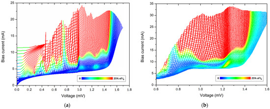
Figure 1.
IVCs of the Nb/Al-AlOx/Nb (a) and the Nb/Al-AlN/NbN (b) FFOs, measured at different magnetic fields. The pumping current of the integrated SIS mixer induced by the FFO radiation is shown by the color.
For most practical applications, continuous frequency tuning of the superconducting local oscillator is required at the arbitrary value of the bias current. This requirement is naturally fulfilled in the flux-flow regime, while in operation in the regime of Fiske steps, stable generation is possible only at Fiske steps, the distance between which in frequency is tens of GHz. This article presents the results of a comprehensive study of the FFO; a method for suppressing Fiske steps was proposed and tested to ensure continuous frequency tuning at voltages V < Vg/3.
It should be noted that spectral measurements by the integrated receiver require not only continuous tuning of the local oscillator frequency, but also the implementation of the FFO phase locking [39]. Considering the delay in the phase locking loop (PLL) between the SIR microcircuit located in the cryostat at helium temperature and the PLL system operating at room temperature, the linewidth of the free-running FFO should not exceed 10–15 MHz to implement synchronization with a sufficiently high spectral quality. The linewidth of the oscillator is proportional to the square of the differential resistance Rd of the FFO at the operating point [40,41,42]; this in turn imposes restrictions on the value of Rd required to implement the PLL regime, therefore special attention should be paid to this problem as Rd is increased for the geometry with the suppression. The purpose of this paper is the development and systematical study of the continuous frequency tunable FFO with low Rd.
2. Materials and Methods
At present, the main elements of superconducting electronics are SIS tunnel structures based on niobium and its compounds. Films made of these materials have high mechanical strength, chemical stability, sustainability to thermal cycling and good adhesion, as well as a sufficiently high critical temperature to operate at liquid helium temperature (T = 4.2 K). The critical temperatures of the films made of niobium and niobium nitride (NbN) are 9.2 K and 15.5 K, respectively. The technology of Nb tunnel junctions with an Al interlayer is based on the well-known fact that a very thin Al layer completely covers the Nb base electrode [43,44,45,46,47], effectively wetting the columnar microstructure of the Nb film and flattening the surface [45] in spite of its roughness. The tunnel barrier is formed by the oxidation or nitridization of a thin aluminum film (5–7 nm), which covers the niobium surface as a continuous layer and makes it possible to obtain ultrathin tunnel layers (about 1 nm thick). The possibility of fabricating the tunnel junctions with high current density and extremely low leakage, which do not change their characteristics for many years, is the most important factor that ensures the widespread use and practical application of junctions based on niobium.
Fabrication technology of multilayer superconducting circuits based on Nb-AlOx-Nb junctions made by Selective Niobium Etching and Anodization Process (SNEAP) [46] was developed and implemented at Kotelnikov Institute of Radio Engineering and Electronics of Russian Academy of Science. A number of new technological processes and techniques for manufacturing superconducting tunnel junctions with unique parameters have been developed [47,48]. Tunnel junctions with high current density allow increasing the operating frequency of SIS receivers and expanding their bandwidth. However, there is a limit to the transparency of the barrier for SIS junctions based on alumina. This limit is of the order of 10–15 kA/cm2; with a further increase in the current density, a sharp degradation of the quality of the junctions occurs. In order to overcome this limitation, a technology for manufacturing Nb/Al-AlN/Nb SIS tunnel junctions with extremely high transparency of the tunnel barrier by nitridization of the Al surface in an RF plasma discharge with acceptable values of the ratio of the subgap to normal resistance (quality parameter Rj/Rn) was developed [49,50,51,52].
Application of NbN as the upper electrode in a three-layer structure made it possible not only to achieve a critical current density up to 70 kA/cm2, but also to significantly improve the parameters of the tunnel structures. As a result, the value of the gap voltage of the Nb-AlN-NbN junctions as high as 3.7 mV was obtained; the quality parameter Rj/Rn exceeds 20 even at high current densities [4,29,52], which indicates the perfect quality of the tunnel barrier. A technology has been developed for manufacturing integrated circuits based on Nb-AlN-NbN tunnel junctions with niobium wiring, which makes it possible to use the advantages of Nb-AlN-NbN junctions in circuits with a topology designed and tested earlier for niobium structures. Using this technology, circuits for studying the linewidth of a superconducting local oscillator, microcircuits of an integrated submm wave spectrometer, and a number of other unique elements and devices were made [4,18,19,20,21,22,23,53]. For the formation of tunnel structures of submicrometer sizes (down to 100 nm), methods of electron-beam lithography were used [54].
The Nb-AlOx-Nb and Nb-AlN-NbN structures were deposited layer by layer in a single vacuum cycle on a silicon substrate, covered with a protective (buffer) layer of Al2O3. Furthermore, by the means of photolithography and plasma etching, the areas of SIS junctions were formed on the surface of the workpiece. During the manufacturing process, the structure went through an isolation stage. It included anodization of the area uncovered by photoresist and magnetron sputtering of the SiO2 layer. This minimized the probability of leakage and shorts for the multilayer structures. The next step was the formation of absorbing resistors by magnetron sputtering of Mo metal (see Section 3.2). The Nb film, which is the top electrode, and Au contact pads, were finally deposited by magnetron sputtering. Detailed descriptions and all main parameters of the technological processes were published in various articles [4,29,47,54].
3. Results and Discussion
3.1. Traditional FFO
First, we describe the operation principles of a traditional FFO based on the LJJ. A DC bias current IB is applied through the LJJ in combination with an external magnetic field, which is generated by the current through the superconducting control line parallel to the junction plane. The magnetic field penetrates into the junction at the end: the Josephson phase φ(x), along the junction changes, with the formation of a vortex carrying the magnetic flux quantum . The bias current causes this quantum to move, and as a result, a unidirectional viscous flow of Josephson vortices arises in the junction, and each vortex has a length of along the junction plane and in the direction perpendicular to the junction plane. The value of the Josephson penetration depth λJ depends on critical current density jc; typically, λJ is of about 5 µm for the jc = 5 kA/cm2, while the London penetration depth for niobium films is 85 nm. Moving along the junction under the Lorentz force, the fluxons are repelled from each other and form a chain of vortices, which is quite rigid at high magnetic fields [55,56]. When a moving fluxon crosses the end of the junction, a voltage pulse V occurs, the integral of which over time is equal to the value of the “emerging” magnetic flux quantum:
The speed and density of this fluxon chain, and, consequently, the power and frequency of electromagnetic radiation that occurs when quanta cross the boundary, can be tuned by changing the bias current Ib and the current through the magnetic field control line ICL. After the vortex collides with the emitting end, a reflected electromagnetic wave arises inside the junction. For a small value of the parameter α, which characterizes the attenuation in the FFO, the wave can reach the opposite end of the junction. At certain frequencies, a standing wave can arise, which will affect the entry of vortices into the junction; as a result, the IVCs in the region of small α has a pronounced resonant structure. The smaller the α, the steeper the current steps appear on the IVC. At higher operating frequencies, the parameter α experiences an abrupt increase due to the effect of Josephson self-pumping [33,34,35,36], and a non-resonant mode of motion of a dense flow of vortex chain is formed (see Section 1). The transition between the two operating modes of the FFO is clearly visible on the IVC (Figure 1 and Figure 2) at voltages V = Vg/3.
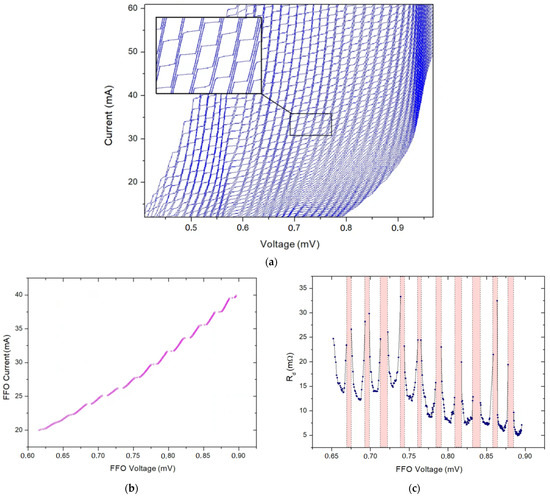
Figure 2.
(a) IVCs of the Nb-AlOx-Nb FFO measured at different magnetic fields induced by the current in integrated control line (ICL = 20–40 mA); (b) IVC of the Nb-AlOx-Nb FFO measured at fixed value of ICL = 29.6 mA; (c) differential resistance Rd calculated from (b) using linear fitting of the IVC over 3 points at each voltage value.
For the successful operation of the superconducting oscillator as a local oscillator (LO) in the integrated receiver [17,18], continuous tuning of the FFO frequency in the entire available frequency range of the device is necessary; in addition, to implement the PLL mode, the linewidth of the FFO emission should not exceed 10–15 MHz. The linewidth of the Josephson junction is determined by the combination of thermal and shot noise in the tunnel junction, which translates into frequency fluctuations at the tunnel junction by the square of differential resistance Rd; exact expression depends on the specific LJJ model [40,41,42,55]. For a current-biased lumped Josephson tunnel junction at temperature T, the full linewidth at half power δf is given by the expression:
δf = 4 π kB T Rd2 Ib/(Φ0 V).
The noise phenomenon observed in Josephson oscillators has been studied since 1980 [57], in addition to the extra noise that can appear for Josephson junctions with high critical current density [58]. A significant increase in the spectral linewidth is due to the effect of noise self-pumping [59,60,61] and transition to the chaotic regime [62,63]. A detailed discussion of these effects is beyond the scope of this article.
Figure 2a shows the IVCs of the Nb-AlOx-Nb junction measured at different magnetic fields, while Figure 2b demonstrates one IVC taken at a fixed magnetic field. The dependence of the differential resistance Rd on voltage V for the curve from Figure 2b is presented in Figure 2c. One can see that there are jumps between steps that make operation impossible in some frequency ranges (marked by bars in Figure 3c). Furthermore, at the edges of the steps, regions of a sharp increase in the differential resistance appear, which leads to a significant broadening of the emission line. The special shape of the FFO [64] is beneficial for suppression on the Fiske steps in the Josephson junctions. We used the same shape for the ends of the FFO (see Figure 3); although in the range of magnetic fields required for the FFO operation, the Fiske steps were still presented on the FFO IVCs. It should be mentioned that continuous frequency tuning and even phase locking with spectral ratio up to 90% was realized for specially designed Nb-AlN-NbN FFO in the frequency range 490–606 GHz (below Vg/3) [18,29]. It became possible due to FFO IVCs bending at low Ib and high voltages (just below Vg/3) caused by dispersion and surface losses [65] by using a specially developed procedure to find the optimal Fiske step nearest to required LO frequency [18,19].
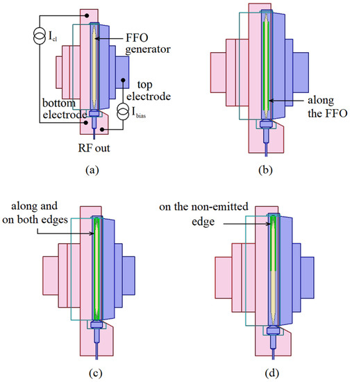
Figure 3.
Layout of the FFO of different designs: (a) traditional FFO; (b) design with resistive layers along the FFO; (c) resistive layers along and on both ends of the FFO; (d) resistive layers on the non-emitting end of the FFO.
3.2. Suppression of Resonant Features. Study of the Modified FFO
In order to “smooth” the IVC of the FFO in the resonant mode, it is necessary to increase the damping parameter α, which would cause the dissipation of the reflected electromagnetic wave inside the junction. This was achieved by introducing an additional resistive layer into the FFO topology. To study the effect of the suppression of the resonances experimentally, several versions of the oscillators were fabricated with a 60–100 nm thick Mo absorber layer, partially covering the FFO and located either along the entire junction or at the FFO ends [66]. Figure 3 shows a schematic representation of the structures with different geometries of absorbing resistors. For a direct comparison, the FFOs without an absorber (see Figure 3a) were fabricated in the same technological run. It should be mentioned that all test circuits contained a small SIS junction to detect the radiation emitted by the FFO [39,67]; this makes it possible to compare the power produced by FFOs with and without absorbers. Both Nb-AlOx-Nb and Nb-AlN-NbN circuits were fabricated and tested.
The location of the resistive layers along the FFO on its sides (Figure 3b) does not provide complete suppression of geometric resonances. There are still weakly expressed regions with a characteristic stepped structure on the IVC in the resonant mode. The inclusion of additional resistors on both ends of the generator and along the FFO (Figure 3c) allows for the suppression of the resonances completely, but leads to strong losses, since only part of the power generated by the FFO reaches the mixer (especially at high frequencies). The location of the resistors only at the non-radiating end where the fluxons enter the FFO (Figure 3d) results in good suppression of resonances and does not lead to considerable additional power losses.
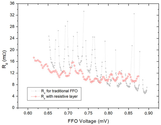
The I–V characteristics of the FFO equipped with absorbing layers placed on the non-radiating end are shown in Figure 4a,b. It can be seen that the dependence became smooth, even in the resonant operating mode. Dependence of the differential resistance Rd on voltage V for the curve from Figure 4b is presented in Figure 4c. Comparison of the Rd-V dependencies for two different designs Figure 3a,d is presented in Figure 5. It is clearly seen that the Rd-V dependence has become smoother without sharp jumps, therefore making it possible to smoothly tune the frequency of the FFO at an arbitrary bias current. This was confirmed by direct measurements of the FFO linewidth (see Section 3.4).
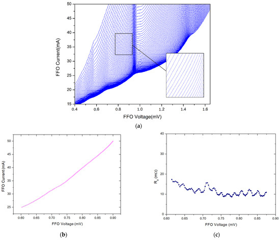
Figure 4.
(a) IVCs of the Nb-AlOx-Nb FFO with resistive layers on the non-emitting end of the FFO (Figure 3d) measured at different magnetic fields induced by the current in integrated control line (ICL = 20–40 mA); (b) one of the FFO IVC measured at fixed value of ICL = 27.2 mA; (c) differential resistance calculated from Figure 4b.
3.3. Modeling of Suppression Methods and Estimation of Parameters
In order to confirm the physical principles of the suppression of the resonant modes, to determine the factors contributing to the suppression the most, and to optimize the geometry of absorbers (without a significant decrease in radiation power of FFO), we carried out the calculations of different geometries in Ansys HFSS [68].
Unfortunately, HFSS does not have in-built tools to treat superconducting effects, such as the penetration of the magnetic field into the superconducting electrodes and the change in propagation velocity due to this effect (Swihart velocity) [30]. In the article by Belitsky et al. [69], the procedure of modeling of the superconducting microstrip line is described. The authors propose to assign special boundary conditions to the corresponding surfaces of the superconductors. In our work, we followed this method. Assigned to the surfaces of superconductors frequency-dependent datasets were generated separately using the expressions of the Mattis–Bardeen theory [70], extended by Zimmermann et al. [71] by taking into account a finite mean free path time of the quasiparticles. In our simulations, we consider a model of Josephson transmission line (JTL).
Figure 6 depicts the geometries of the simulated structures. When fabricating the junction, the narrowing regions near its ends were carried out to provide better coupling of the FFO with the outer circuit and to decrease the reflection from the end of the FFO. In geometries 2 and 3, the metal layer overhung the junction and due to this geometry, the field leaked out of the junction. We modeled only the “input” part of the FFO where fluxons enter the junction; we assigned a single lumped port for JTL excitation, as shown in Figure 6. This enabled us, on one hand, to investigate the absorption of the electromagnetic waves in the line, and on the other hand, to examine the reflection of the wave from the end of the junction. We could assign the port impedance to match the line in order to avoid reflections, but dispersion in the line at high frequencies due to the change in London penetration depth and geometrical factor made this task almost impossible. As is shown later, it turned out to be much easier to set the impedance of the excitation port much bigger than the characteristic impedance of the line (impedance of the port was set to 100 Ω and the characteristic impedance of the line was around 0.3 Ω) and then recalculate the data on S11 in order to eliminate the influence of the port.
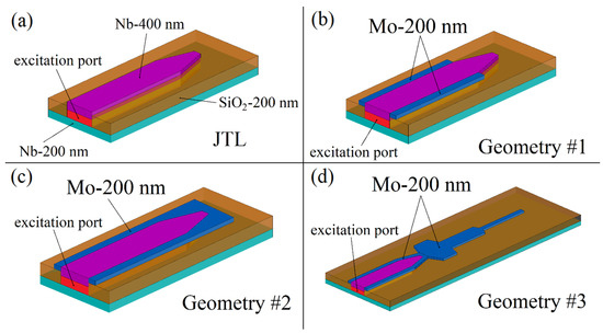
Figure 6.
3D-models of the simulated geometries. (a) FFO without idle region (geometry #0, corresponds to Figure 3a); (b) geometry with normal metal layer along the FFO where width is constant (geometry #1, Figure 3b); (c) circuit with normal metal layer at the end and along the junction (#2, Figure 3d); (d) design with the impedance transformer connected to the end (#3) in order to decrease the reflection.
The results of the simulation are shown in Figure 7 where the lines represent the magnitude of S11-parameter dependence on frequency. It is clearly seen that the application of the normal metal to the idle region leads to a strong decrease in amplitude of the oscillations which corresponds to the absorption of radiation in the structure. Moreover, when adding normal metal to the end of the FFO, almost complete suppression of the resonances can be obtained (see green curve, which refers to geometry #2 and corresponds to the experimental layout presented in Figure 3d).
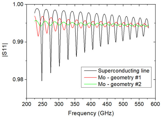
Figure 7.
S11-parameter dependence on frequency from simulations in Ansys HFSS. Black curve represents the result for barely superconducting line; red curve depicts the geometry with normal metal in idle region, but with uncovered end; green corresponds to the geometry with normal metal both near the line and at the end (see Figure 6).
Here, we derive some formulas in order to eliminate the reflections from the excitation port and quantitatively estimate the level of attenuation in the line and reflection ratio from the ends in the investigated structures. Consider an incident wave coming from the left; it reflects from the outer boundary of the line with the amplitude reflection ratio r1, which is given by the well-known expression:
where Zline and Zport denote the characteristic impedance of the line and the impedance of the port. Amplitude of the wave decreases exponentially with the distance due to the absorption in the line. Reflection ratio from the opposite end is r2. Taking all the effects above into account, we can derive the expression for S11:
where κ is the attenuation constant, k is the wave number k = 2π/λ, and L is the length of the line; in the first term denotes that the port impedance is larger than that of the line. This expression can be rewritten for the magnitude of S11:
where .
The magnitude of S11 reaches its maxima when cos(2kL) = 1 and minima when cos(2kL) = −1. Corresponding expressions are:
Thus, the difference between maxima and minima is given by formula:
By taking a natural logarithm of the expression for diff and expanding it into a Taylor series, assuming , being small compared to unity, we obtain:
Thus, the magnitude of the oscillations of |S11| in this case is almost completely determined (with an error less than 15% for superconducting case and 2% for all the other simulations) by the absorption in the line and reflection ratio from the opposite boundary as the term in square brackets can be neglected. Yet, there is a value C(r1) in the expression above which is the same for all simulated geometries and can be determined by the extrapolation of the curve corresponding the superconducting case to the low-frequency region.
This enables us to determine the amplitude of the wave after passing through the structure. Recalculated curves in a format: , where B1 is an amplitude of the wave returned to the port after propagation in the line and reflection from the end, and A1 is the initial amplitude, are shown on Figure 8. For all the geometries, an increase in the attenuation with frequency is observed as expected. This can be explained by two factors. First, the wave number and the attenuation constant depend linearly on frequency [72]. Second, the resistance of the films made either of a superconductor or normal metal increases with frequency [70,71]; this leads to stronger absorption of electromagnetic wave energy in the structures. The introduction of layers of normal metal to the idle region of the junction leads to a decrease in the magnitude of the reflected wave by a factor of 4 (curve Mo #1); an additional normal metal layer at the end of the junction improves this result to more than the order of magnitude (curve Mo #2) in the whole frequency range 200–500 GHz.
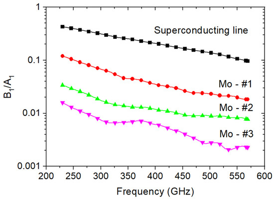
Figure 8.
Amplitude of the wave after propagation in the line and reflection from the end normalized to the initial amplitude versus frequency for simulated structures.
It should be noted that attenuation layers significantly reduce the radiation power of the FFO. Thus, it is crucial to design a geometry with a low reflection ratio from the ends and low losses. As we can see from Figure 6 and Figure 8, the suppression of the resonances can be improved, either by the attenuation layers near the line or by the modifications of the end (compare geometries #2 and #1). Therefore, we designed and performed a simulation of the structure with a Chebyshev impedance transformer connected to the end of the structure. The transformer was optimized to provide a match between the FFO and outer medium at frequency 300 GHz. Both the structures made of a superconductor and normal metal were simulated. In the structure with the superconducting transformer, any noticeable change in damping compared to geometry #2 was observed, but geometry with the transformer made of normal metal showed an additional decrease in amplitude by more than two times (see Mo-#3 curve in Figure 8).
However, many effects regarding the real FFO are yet to be considered in simulations. First, our simulation did not involve any effects related to the fluxon dynamics and generation in the FFO. Actually, the generation occurred only when the fluxon reached the end of the junction and far from the ends the FFO behaved like a passive transmission line. However, standard excitation port in Ansys HFSS was still a good approximation. Second, in a real structure, there is an overlapping region made of a superconductor, which covers the FFO itself and the metallization layers (in corresponding geometries). As shown in a study by Lee et al. [65], this may greatly contribute to the propagation velocity depending on the width of the overlap. Moreover, the proximity effect [73] significantly impacts the properties of normal metal and poses some restrictions on the layer thickness.
3.4. Measurements of the FFO Radiation
In practice, the most accurate measurements of Rd are made by recording spectra of the FFO emission line; the measuring technique is described in the papers [28,39,67]. The oscillator under study was part of an integrated microcircuit also comprising a small SIS junction with an area of about 1.5 μm2 to monitor the radiation of the FFO, and specially designed matching and tuning elements. The superconducting microcircuit was mounted inside a helium cryostat equipped with the necessary electronics for DC and microwave measurements. The SIS junction located on the same chip with the FFO was also used as a harmonic mixer (HM) with a very high harmonic number up to 50. The emission from the FFO under testing and the signal from the reference synthesizer (which is at room temperature, = 10–20 GHz met at the harmonic mixer. At the output of the HM, a signal appeared at the intermediate frequency (IF) fIF, equal to the difference between the frequency of the FFO, fFFO, and the nth harmonic of the reference synthesizer fsynth.
Next, the output HM signal traveled to a cryogenic high electron mobility transistors (HEMT) amplifier, then to a warm IF amplifier that was at room temperature. Thus, the signal from a superconducting local oscillator was downconverted and recorded by a spectrum analyzer. By using this technique, it was possible to record FFO IVCs and determine FFO differential resistance with very high accuracy by using Josephson relation: FFO frequency can be measured by a spectrum analyzer with an accuracy of about 1 MHz that corresponds to 2 nV precision for voltage reading. By measuring the FFO bias current for two points with a certain frequency shift (e.g., 500 MHz, which corresponds to a voltage shift of about 1 µV), the Rd value can be determined. The results are presented in Figure 9a,b for two FFO frequencies.
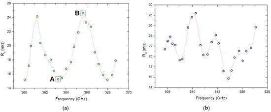
Figure 9.
Dependencies of the FFO differential resistance Rd on FFO frequency recorded for the Nb-AlN-NbN junction by spectra measuring technique in two frequency ranges; near 365 (a) and 515 GHz (b). Experimental points are connected by lines as a guide for the eye.
By using a technique based on an integrated harmonic mixer described above [17,28,39,67], it was possible to the measure free-running linewidth of the FFO at each point, providing frequency stabilization to compensate for low-frequency noise temperature fluctuations. The results are presented in Figure 10, which shows down-converted emission spectra measured in two points, marked in Figure 9 by labels “A” and “B”; the linewidth varies from 4 MHz to 12 MHz due to the change in the value of Rd using a specially developed technique [28,39,67]. Dependence of the FFO linewidth versus frequency is shown in Figure 11. The linewidth does not exceed 12 MHz at all operating points, making FFO phase locking PLL possible [28,39,67]; phase-locked spectra of the FFO are shown in Figure 10, along with free-running FFO spectra. Thus, the proposed approach ensured the smooth tuning of the oscillator frequency and provided the possibility for phase locking of the FFO for any frequency at a constant bias current.
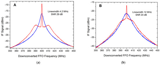
Figure 10.
Down-converted spectra of the Nb-AlN-NbN FFO recorded for points A and B (see Figure 9); spectra are measured for free-running and phase-locked FFO (blue and red curves, respectively).
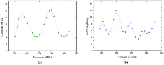
Figure 11.
Dependencies of the free-running FFO linewidth on FFO frequency recorded for frequency ranges near 365 (a) and 515 GHz (b). Experimental points are connected by lines as a guide for the eye.
4. Conclusions
We proposed and realized a method for suppressing resonances in a sub-terahertz superconducting local oscillator based on long Josephson junctions. The suggested method is based on the introduction of normal metal layers near the junction. Modeling of the propagation of electromagnetic waves in the proposed integrated circuits was performed; experimental samples were fabricated and tested. Complete suppression of resonances and the possibility of continuous tuning of the frequency of a superconducting local oscillator in the range of 200–700 GHz at arbitrary bias current have been demonstrated. The linewidth of the FFO radiation in the range 4–12 MHz was measured, allowing the realization of FFO phase locking, which is vitally important for spectral studies. Geometry with a matching circuit made of normal metal connected to one of the ends of the FFO was proposed and modeled. This geometry will help to improve the suppression even further, without a significant change in losses compared with the standard FFO geometry.
5. Patents
This study is based on the Patent by Paramonov M.E., Filippenko L.V, Fominsky M.Yu, Koshelets V.P. “Cryogenic Tunable Oscillator of Sub-Terahertz Range Heterodyne for Integrated Receiving Systems”; Patent RU2638964 (C1) [51].
Author Contributions
Conceptualization and methodology, V.P.K.; FFO and SIS circuit fabrication, L.V.F.; IVC and LW measurements, M.E.P., O.S.K. and V.P.K.; electromagnetic simulations, F.V.K.; data analysis, writing and editing, L.V.F., F.V.K., M.E.P., O.S.K. and V.P.K. All authors have read and agreed to the published version of the manuscript.
Funding
The work was supported by the Russian Foundation for Basic Research (grant No. 19-52-80023). The development and fabrication of the FFO circuits was supported by the State Assignment of the Kotelnikov IRE RAS (project FFWZ-2022-0005). The equipment of USU “Cryointegral” was used to carry out the research; USU is supported by a grant from the Ministry of Science and Higher Education of the Russian Federation, agreement No. 075-15-2021-667.
Conflicts of Interest
The authors declare no conflict of interest.
References
- Zmuidzinas, J.; Richards, P.L. Superconducting detectors and mixers for millimeter and submillimeter astrophysics. Proc. IEEE 2004, 92, 1597–1616. [Google Scholar] [CrossRef]
- De Graauw, T.; Helmich, F.P.; Phillips, T.G.; Stutzki, J.; Caux, E.; Whyborn, N.D.; Dieleman, P.; Roelfsema, P.R.; Aarts, H.; Assendorp, R.; et al. The Herschel—Heterodyne Instrument for the Far-Infrared (HIFI). Astron. Astrophys. 2010, 518, 1–7. [Google Scholar] [CrossRef]
- ALMA Observatory Website. Available online: https://www.almaobservatory.org/en/about-alma/ (accessed on 27 July 2022).
- Dmitriev, P.N.; Filippenko, L.V.; Koshelets, V.P. Applications in Superconducting SIS Mixers and Oscillators: Toward Integrated Receivers. In Josephson Junctions, History, Devices, and Applications; Wolf, E., Arnold, G., Gurvitch, M., Zasadzinski, J., Eds.; Pan Stanford Publishing Pte: Singapore, 2017; pp. 185–244, ISBN1 978-981-4745-47-5 (Hardcover), ISBN2 978-1-315-36452-0 (eBook). [Google Scholar]
- Ustinov, A.V.; Kohlstedt, H.; Heiden, C. Possible phase locking of vertically stacked Josephson flux-flow oscillators. Appl. Phys. Lett. 1994, 65, 1457–1459. [Google Scholar] [CrossRef]
- Darula, M.; Doderer, T.; Beuven, S. Millimetre and sub-mm wavelength radiation sources based on discrete Josephson junction arrays. Supercond. Sci. Technol. 1999, 12, R1–R25. [Google Scholar] [CrossRef]
- Jain, A.K.; Likharev, K.K.; Lukens, J.E.; Sauvageau, J.E. Mutual phase-locking in Josephson junction arrays. Phys. Rep. 1984, 109, 309–426. [Google Scholar] [CrossRef]
- Kleiner, R.; Müller, P. Intrinsic Josephson effects in high-T c superconductors. Phys. Rev. B 1994, 49, 1327–1342. [Google Scholar] [CrossRef]
- Ozyuzer, L.; Koshelev, A.E.; Kurter, C.; Gopalsami, N.; Li, Q.; Tachiki, M.; Kadowaki, K.; Yamamoto, T.; Minami, H.; Yamaguchi, H.; et al. Emission of coherent THz radiation from superconductors. Science 2007, 318, 1291–1293. [Google Scholar] [CrossRef]
- Barbara, P.; Cawthorne, A.B.; Shitov, S.V.; Lobb, C.J. Stimulated emission and amplification in Josephson junction arrays. Phys. Rev. Lett. 1999, 82, 1963–1966. [Google Scholar] [CrossRef]
- Welp, U.; Kadowaki, K.; Kleiner, R. Superconducting emitters of THz radiation. Nat. Photonics 2013, 7, 702–710. [Google Scholar] [CrossRef]
- Tucker, J.R. Quantum Limited Detection in Tunnel Junction Mixers. IEEE J. Quantum Electron. 1979, 15, 1234–1258. [Google Scholar] [CrossRef]
- Tucker, J.R.; Feldman, M.J. Quantum Detection at millimeter wavelengths. Rev. Mod. Phys. 1985, 57, 1055–1113. [Google Scholar] [CrossRef]
- Baryshev, A.M.; Hesper, R.; Mena, F.P.; Klapwijk, T.M.; van Kempen, T.A.; Hogerheijde, M.R.; Jackson, B.D.; Adema, J.; Gerlofsma, G.J.; Bekema, M.E.; et al. The ALMA Band 9 receiver. Design, construction, characterization, and first light. Astron. Astrophys. 2015, 577, A129. [Google Scholar] [CrossRef]
- Rudakov, K.I.; Khudchenko, A.V.; Filippenko, L.V.; Paramonov, M.E.; Hesper, R.; da Costa Lima, D.A.R.; Baryshev, A.M.; Koshelets, V.P. THz Range Low-Noise SIS Receivers for Space and Ground-Based Radio Astronomy. Appl. Sci. 2021, 11, 10087. [Google Scholar] [CrossRef]
- Karpov, A.; Miller, D.; Rice, F.; Stern, J.A.; Bumble, B.; LeDuc, H.G.; Zmuidzinas, J. Low Noise 1 THz–1.4 THz Mixers Using Nb/Al-AlN/NbTiN SIS Junctions. IEEE Trans. Appl. Supercond. 2007, 17, 343–346. [Google Scholar] [CrossRef]
- Koshelets, V.P.; Shitov, S.V. Integrated Superconducting Receivers. Supercond. Sci. Technol. 2000, 13, R53–R69. [Google Scholar] [CrossRef]
- Koshelets, V.P.; de Lange, A.; de Lange, G.; Vaks, V.L.; Li, M.Y.; Wang, H.; Dmitriev, P.N.; Faley, M.I.; Filippenko, L.V.; Kalashnikov, K.; et al. Superconducting Integrated Terahertz Spectrometers. IEEE Trans. Terahertz Sci. Technol. 2015, 5, 687–694. [Google Scholar] [CrossRef]
- De Lange, G.; Birk, M.; Boersma, D.; Dercksen, J.; Dmitriev, P.; Ermakov, A.; Filippenko, L.; Golstein, H.; Hoogeveen, R.; de Jong, L.; et al. Development and characterization of the superconducting integrated receiver channel of the TELIS atmospheric sounder. Supercond. Sci. Technol. 2010, 23, 045016. [Google Scholar] [CrossRef]
- Li, M.; Yuan, J.; Kinev, N.; Li, J.; Gross, B.; Guénon, S.; Ishii, A.; Hirata, K.; Hatano, T.; Koelle, D.; et al. Linewidth dependence of coherent terahertz emission from Bi2Sr2CaCu2O8 intrinsic Josephson junction stacks in the hot-spot regime. Phys. Rev. B 2012, 86, 060505. [Google Scholar] [CrossRef]
- Sobakinskaya, E.; Vaks, V.L.; Kinev, N.; Ji, M.; Lia, M.Y.; Wang, H.B.; Koshelets, V.P. High-resolution terahertz spectroscopy with a noise radiation source based on high-Tc superconductors. J. Phys. D Appl. Phys. 2017, 50, 035305. [Google Scholar] [CrossRef]
- Baksheeva, K.; Ozhegov, R.; Goltsman, G.; Kinev, N.; Koshelets, V.; Kochnev, A.; Betzalel, N.; Puzenko, A.; Ishai, P.; Feldman, Y. The Sub THz Emission of the Human Body under Physiological Stress. IEEE Trans. Terahertz Sci. Technol. 2021, 11, 381–388. [Google Scholar] [CrossRef]
- Kinev, N.V.; Rudakov, K.I.; Filippenko, L.V.; Baryshev, A.M.; Koshelets, V.P. Terahertz spectroscopy of gas absorption using the superconducting flux-flow oscillator as an active source and the superconducting integrated receiver. Sensors 2020, 20, 7267. [Google Scholar] [CrossRef] [PubMed]
- Nagatsuma, T.; Enpuku, K.; Irie, F.; Yoshida, K. Flux-flow type Josephson oscillator for millimeter and submillimeter wave region. J. Appl. Phys. 1983, 54, 3302–3309. [Google Scholar] [CrossRef]
- Nagatsuma, T.; Enpuku, K.; Yoshida, K.; Irie, F. Flux-flow-type Josephson oscillator for millimeter and submillimeter wave region. II. Modeling. J. Appl. Phys. 1984, 56, 3284–3293. [Google Scholar] [CrossRef]
- Nagatsuma, T.; Enpuku, K.; Sueoka, K.; Yoshida, K.; Irie, F. Flux-flow-type Josephson oscillator for millimeter and submillimeter wave region. III. Oscillation stability. J. Appl. Phys. 1985, 58, 441–449. [Google Scholar] [CrossRef]
- Qin, J.; Enpuku, K.; Yoshida, K. Flux-flow-type Josephson oscillator for millimeter and submillimeter wave region. IV. Thin-film coupling. J. Appl. Phys. 1988, 63, 1130–1135. [Google Scholar] [CrossRef]
- Koshelets, V.P.; Dmitriev, P.; Ermakov, A.; Sobolev, A.; Torgashin, M.; Kurin, V.; Pankratov, A.; Mygind, J. Optimization of the Phase-Locked Flux-Flow Oscillator for the submm Integrated Receiver. IEEE Trans. Appl. Supercond. 2005, 15, 964–967. [Google Scholar] [CrossRef]
- Torgashin, M.Y.; Koshelets, V.P.; Dmitriev, P.N.; Ermakov, A.B.; Filippenko, L.V.; Yagoubov, P.A. Superconducting integrated receiver based on Nb-AlN-NbN-Nb circuits. IEEE Trans. Appl. Supercond. 2007, 17, 379–382. [Google Scholar] [CrossRef]
- Swihart, J.C. Field solution for a thin-film superconducting strip transmission line. J. Appl. Phys. 1961, 32, 461–469. [Google Scholar] [CrossRef]
- Enpuku, K.; Yoshida, K.; Irie, F. Self-resonant current steps of Josephson tunnel junctions in the presence of multimode oscillation. J. Appl. Phys. 1981, 52, 344–351. [Google Scholar] [CrossRef]
- Erne, S.N.; Ferrigno, A.; Parmentier, R.D. Fluxon propagation and Fiske steps in long Josephson tunnel junctions. Phys. Rev. B 1983, 27, 5440–5446. [Google Scholar] [CrossRef] [Green Version]
- Koshelets, V.P.; Shitov, S.V.; Shchukin, A.V.; Filippenko, L.V.; Mygind, J.; Ustinov, A.V. Self-Pumping Effects and Radiation Linewidth of Josephson Flux Flow Oscillators. Phys. Rev. B 1997, 56, 5572–5577. [Google Scholar] [CrossRef]
- Werthamer, N.R. Nonlinear self-coupling of Josephson radiation in superconducting tunnel junctions. Phys. Rev. 1966, 147, 255–263. [Google Scholar] [CrossRef]
- Hasselberg, L.E.; Levinsen, M.T.; Samuelsen, M.R. Theories of subharmonic gap structures in superconducting junctions. Phys. Rev. B 1974, 9, 3757–3765. [Google Scholar] [CrossRef]
- Maezawa, M.; Aoyagi, M.; Nakagawa, H.; Kurosawa, I.; Takada, S. Observation of Josephson self-coupling in Nb AlOx Nb tunnel junctions. Phys. Rev. B 1994, 50, 9664–9667. [Google Scholar] [CrossRef]
- Gulevich, D.R.; Koshelets, V.P.; Kusmartsev, F.V. Josephson flux-flow oscillator: The microscopic tunneling approach. Phys. Rev. B 2017, 96, 024515. [Google Scholar] [CrossRef]
- Gulevich, D.R.; Filippenko, L.V.; Koshelets, V.P. Microscopic Tunneling Model of Nb–AlN–NbN Josephson Flux-Flow Oscillator. J. Low Temp. Phys. 2019, 194, 312–324. [Google Scholar] [CrossRef]
- Koshelets, V.P.; Shitov, S.V.; Filippenko, L.V.; Vaks, V.L.; Mygind, J.; Baryshev, A.M.; Luinge, W.; Whyborn, N. Phase locked 270–440 GHz local oscillator based on flux flow in long Josephson tunnel junctions. Rev. Sci. Instrum. 2000, 71, 289–293. [Google Scholar] [CrossRef]
- Dahm, A.J.; Denenstein, A.; Langenberg, D.N.; Parker, W.M.; Rogovin, D.; Scalapino, D.J. Linewidth of the radiation emiited by a Josephson junction. Phys. Rev. Lett. 1969, 22, 1416–1420. [Google Scholar] [CrossRef]
- Joergensen, E.; Koshelets, V.P.; Monaco, R.; Mygind, J.; Samuelsen, M.R.; Salerno, M. Thermal fluctuations in resonant motion of fluxons on a Josephson transmission line: Theory and experiment. Phys. Rev. Lett. 1982, 49, 1093–1096. [Google Scholar] [CrossRef]
- Likharev, K.K. Dynamics of Josephson Junctions and Circuits, 1st ed.; Chapter 4; Gordon and Breach: London, UK, 1986; pp. 105–113. [Google Scholar]
- Rowell, J.M.; Gurvitch, M.; Geerk, J. Modification of tunneling barriers on Nb by a few monolayers of Al. Phys. Rev. B 1981, 24, 2278–2281. [Google Scholar] [CrossRef]
- Gurvitch, M.; Washington, M.A.; Huggins, H.A. High quality refractory Josephson tunnel junctions utilizing thin aluminum layers. Appl. Phys. Lett. 1983, 42, 472–474. [Google Scholar] [CrossRef]
- Imamura, T.; Shiota, T.; Hasuo, S. Fabrication of high quality Nb/AlOx-Al/Nb Josephson junctions: I—Sputtered Nb films for junction electrode. IEEE Trans. Appl. Supercond. 1992, 2, 1–14. [Google Scholar] [CrossRef]
- Kroger, H.; Smith, L.N.; Jillie, D.W. Selective niobium anodization process for fabrication Josephson tunnel junctions. Appl. Phys. Lett. 1981, 39, 280–282. [Google Scholar] [CrossRef]
- Filippenko, L.V.; Shitov, S.V.; Dmitriev, P.N.; Ermakov, A.B.; Koshelets, V.P.; Gao, J.R. Submillimeter superconducting integrated receivers: Fabrication and yield. IEEE Trans. Appl. Supercond. 2001, 11, 816–819. [Google Scholar] [CrossRef]
- Butz, S.; Jung, P.; Filippenko, L.V.; Koshelets, V.P.; Ustinov, A.V. A one-dimensional tunable magnetic metamaterial. Opt. Express 2013, 21, 22540–22548. [Google Scholar] [CrossRef] [PubMed]
- Shiota, T.; Imamura, T.; Hasuo, S. Nb Josephson junction with an AlNx barrier made by plasma nitridation. Appl. Phys. Lett. 1992, 61, 1228–1230. [Google Scholar] [CrossRef]
- Kleinsasser, A.W.; Miller, R.E.; Mallison, W.H. Nb/AIN/Nb Josephson Junctions with High Critical Current Density. IEEE Trans. Appl. Supercond. 1995, 5, 2318–2321. [Google Scholar] [CrossRef]
- Kawamura, J.; Miller, D.; Chen, J.; Zmuidzinas, J.; Bumble, B.; LeDuc, H.G.; Stern, J.A. Very high-current-density Nb/AlN/Nb tunnel junctions for low-noise submillimeter mixers. Appl. Phys. Lett. 2000, 76, 2119–2121. [Google Scholar] [CrossRef]
- Dmitriev, P.N.; Lapitskaya, I.L.; Filippenko, L.V.; Ermakov, A.B.; Shitov, S.V.; Prokopenko, G.V.; Kovtonyuk, S.A.; Koshelets, V.P. High quality Nb-based tunnel junctions for high frequency and digital applications. IEEE Trans. Appl. Supercond. 2003, 13, 107–110. [Google Scholar] [CrossRef]
- Khudchenko, A.; Baryshev, A.M.; Rudakov, K.I.; Dmitriev, P.M.; Hesper, R.; de Jong, L.; Koshelets, V.P. High-Gap Nb-AlN-NbN SIS Junctions for Frequency Band 790-950 GHz. IEEE Trans. Terahertz Sci. Technol. 2016, 6, 127–132. [Google Scholar] [CrossRef]
- Fominsky, M.Y.; Filippenko, L.V.; Chekushkin, A.M.; Dmitriev, P.N.; Koshelets, V.P. Fabrication of Superconducting Nb–AlN–NbN Tunnel Junctions Using Electron-Beam Lithography. Electronics 2021, 10, 2944. [Google Scholar] [CrossRef]
- Golubov, A.A.; Malomed, B.A.; Ustinov, A.V. Radiation linewidth of a long Josephson junction in the flux-flow regime. Phys. Rev. B 1996, 54, 3047–3050. [Google Scholar] [CrossRef] [PubMed]
- Ustinov, A.V.; Kohlstedt, H.; Henne, P. Giant radiation linewidth of multifluxon states in long Josephson junctions. Phys. Rev. Lett. 1996, 77, 3617–3620. [Google Scholar] [CrossRef] [PubMed]
- Huberman, B.A.; Crutchfield, J.P.; Packard, N.H. Noise phenomena in Josephson junctions. Appl. Phys. Lett. 1980, 37, 750–752. [Google Scholar] [CrossRef]
- Dieleman, P.; Bukkems, H.G.; Klapwijk, T.M.; Schicke, M.; Gundlach, K.H. Observation of Andreev reflection enhanced shot noise. Phys. Rev. Lett. 1997, 79, 3486–3489. [Google Scholar] [CrossRef]
- Koshelets, V.P.; Dmitriev, P.N.; Sobolev, A.S.; Pankratov, A.L.; Khodos, V.V.; Vaks, V.L.; Baryshev, A.M.; Wesselius, P.R.; Mygind, J. Line width of Josephson flux flow oscillators. Phys. C Supercond. 2002, 372, 316–321. [Google Scholar] [CrossRef]
- Pankratov, A.L. Noise self-pumping in long Josephson junctions. Phys. Rev. B 2008, 78, 024515. [Google Scholar] [CrossRef]
- Matrozova, E.A.; Pankratov, A.L.; Levichev, M.Y.; Vaks, V.L. Spectral characteristics of noisy Josephson flux flow oscillator. J. Appl. Phys. 2011, 110, 053922. [Google Scholar] [CrossRef]
- Pankratov, A.L.; Pankratova, E.V.; Shamporov, V.A.; Shitov, S.V. Oscillations in Josephson transmission line stimulated by load in the presence of noise. Appl. Phys. Lett. 2017, 110, 112601. [Google Scholar] [CrossRef]
- Gulevich, D.R.; Koshelets, V.P.; Kusmartsev, F.V. Bridging the Terahertz gap for chaotic sources with superconducting junctions. Phys. Rev. B 2019, 99, 060501.1–060501.6. [Google Scholar] [CrossRef] [Green Version]
- Gijsbertsen, J.G.; Houwman, E.P.; Klopman, B.B.G.; Flokstra, J.; Rogalla, H.; Quenter, D.; Lemke, S. Field dependence of the Josephson current and Fiske resonances in specially shaped Josephson junctions. Phys. C Supercond. 1995, 249, 12–14. [Google Scholar] [CrossRef]
- Lee, G.S.; Barfknecht, A.T. Geometric and material dispersion in Josephson transmission lines. IEEE Trans. Appl. Supercond. 1992, 2, 67–73. [Google Scholar] [CrossRef]
- Paramonov, M.E.; Filippenko, L.V.; Fominsky, M.Y.; Koshelets, V.P. Cryogenic Tunable Oscillator of Sub-Terahertz Range Heterodyne for Integrated Receiving Systems. RU Patent RU2638964 (C1), 19 December 2017. [Google Scholar]
- Dmitriev, P.N.; Ermakov, A.B.; Kinev, N.V.; Kiselev, O.S.; Filippenko, L.V.; Fominskii, M.Y.; Koshelets, V.P. Superconducting Structures for Study and Phase Synchronization of Integrated Terahertz Oscillators. J. Commun. Technol. Electron. 2021, 66, 473–479. [Google Scholar] [CrossRef]
- Ansys HFSS. Available online: https://www.ansys.com/products/electronics/ansys-hfss (accessed on 27 July 2022).
- Belitsky, V.; Risacher, C.; Pantaleev, V.; Vassilev, V. Superconducting microstrip line model studies at millimetre and sub-millimetre waves. Int. J. Infrared Millim. Waves 2006, 27, 809–834. [Google Scholar] [CrossRef]
- Mattis, D.C.; Bardeen, J. Theory of the anomalous skin effect in normal and superconducting metals. Phys. Rev. 1958, 111, 412–417. [Google Scholar] [CrossRef]
- Zimmermann, W.; Brandt, E.H.; Bauer, M.; Seider, E.; Genzel, L. Optical conductivity of BCS superconductors with arbitrary purity. Phys. C Supercond. 1991, 183, 99–104. [Google Scholar] [CrossRef]
- Fusco, V.F. Microwave Circuits: Analysis and Computer-Aided Design, 1st ed.; Prentice Hall: Hoboken, NJ, USA, 1987; Chapter 1; pp. 20–23. [Google Scholar]
- Tinkham, M. Introduction to Superconductivity, 2nd ed.; Chapter 6; McGraw-Hill: New York, NY, USA, 2004; pp. 198–205. [Google Scholar]
Publisher’s Note: MDPI stays neutral with regard to jurisdictional claims in published maps and institutional affiliations. |
© 2022 by the authors. Licensee MDPI, Basel, Switzerland. This article is an open access article distributed under the terms and conditions of the Creative Commons Attribution (CC BY) license (https://creativecommons.org/licenses/by/4.0/).