Abstract
The active clamp flyback (ACF) converter is gradually becoming popular in the application field of low or medium output power range due to its advantage of soft switching and high conversion efficiency. An asymmetric half-bridge (AHB) flyback converter has been proposed in previous studies. The main advantages of the AHB flyback are the same number of components as the ACF converter and the soft switching technique. In this paper, an AHB flyback converter with constant off-time (COT) plus pulse frequency modulation (PFM) is proposed, so that the resonant time is not affected by the input voltage and load, and can achieve a wide range of zero voltage switching (ZVS) operating range. Compared to pulse width modulation (PWM), the PFM control with COT can make the system more stable. Finally, a prototype circuit with a specification input of 48 V to an output of 2.5 V/8 A is made for verification.
1. Introduction
The flyback converter is widely used in the low to medium output power range because of the advantages of fewer circuit components and simple control. Compared with the LLC converter, the flyback converter requires fewer components, but the switching voltage stress of the flyback converter is higher than that of the LLC converter. The voltage stress of the main switch of the flyback converter is the input voltage plus the reflection voltage and spike voltage. The snubber circuit is added to switches of the flyback converter to reduce the voltage surge. However, the voltage stress of an LLC converter is only equal to the input voltage, so low-voltage components can be used. The advantage of flyback converter over LLC converter is the wide input voltage and the simple control method, so that no pre-stage voltage regulator is required. Although the research in [1,2] provides the input voltage range with wide variation range of switching frequency, it also results in efficiency reduction and EMI problems. The multi-level approaches proposed in [3,4,5,6,7,8,9,10,11] make LLC converters extend the operating voltage range, but still have the problems of the number of components, complex structure, and difficult control, so as to make it difficult to balance cost and performance. Based on the reasons above, the flyback-based topologies are still attractive solutions.
To increase conversion efficiency, more technologies have been added to the conventional flyback converter, such as quasi-resonance (QR) [12,13,14,15] or active clamping [16,17,18,19] to achieve zero-voltage switching (ZVS) and reduce switching loss. Synchronous rectification (SR) [20,21] can also be applied to reduce the conduction loss and further improve the conversion efficiency. The difference in the number of components between the active clamp flyback (ACF) converter and the LLC converter is that the ACF converter needs only a single secondary SR switch, which is the cost advantage of the ACF converter.
The asymmetric half-bridge (AHB) flyback converter has been proposed in previous studies [20,21,22,23,24,25,26,27,28,29], whose main advantage is that the number of components is the same as that of ACF converter, and it also provides the same voltage stress on the switching elements as the LLC converter with ZVS turn-on. Most studies of AHB flyback converters adopt pulse width modulation (PWM) control.
However, previous researches in [20,21,22,23,24,25,26,27] suggest that PWM should not be used because Toff of PWM mode varies with the input voltage and load condition to affect the ZVS operation range. In [28], the AHB flyback converter is unstable with the PWM control method. The article [20,30] proposes a resonant AHB flyback, which provides a ZVS function on its switches. However, the efficiency at light load and dynamic response are not mentioned.
The resonant high step-down converter [31], shown in Figure 1, is proposed with constant off-time (COT) and pulse frequency modulation (PFM), which is verified with a wide range of ZVS operations. In this paper, a resonant AHB flyback converter with COT control is proposed as shown in Figure 2 to improve the ZVS operation. A prototype with a specification input of 48 V to output 2.5 V/8 A is made to verify that the concept is feasible.
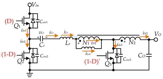
Figure 1.
The previous high step-down converter with COT control.
Figure 2.
The proposed resonant AHB flyback converter.
2. Proposed Circuit Configuration
As shown in Figure 2, the proposed circuit consists of half-bridge switches Q1 and Q2, a SR switch Q3, resonant capacitor Cr, and coupling inductor L with magnetizing inductance Lm, leakage inductor Lr, and windings N1 and N2. The proposed circuit adopts the combinational control method of QR and COT [31], which is suitable for a converter with low voltage gain and high output current. Figure 3 shows the waveforms of each point of the circuit. The proposed circuit has 8 states, as shown in Figure 4.
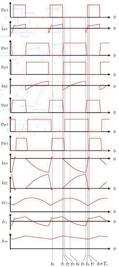
Figure 3.
Operation waveforms of the proposed circuit.
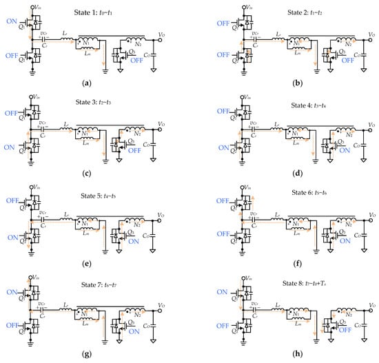
Figure 4.
Operation states of the proposed circuit: (a) state 1; (b) state 2; (c) state 3; (d) state 4; (e) state 5; (f) state 6; (g) state 7; and (h) state 8.
Before entering the following behavior description, the definitions of the resonance tanks are listed as (1) to (8). In addition, the iN2(0) and the ids2(0) are both supposed as 0 A at t0, respectively. The inductance of Lm is assumed to be much higher than the inductance of Lr, so iLm can be considered a constant current source.
2.1. State 1 (t0 − t1)
During this interval, Q1 is turned on, and Q2 and Q3 are turned off. Vin charges Cr and magnetizes Lm to make iLm (iLm = iLr = iCr) rise. When Q1 is turned off, it enters state 2.
2.2. State 2 (t1 − t2)
During this interval, Q1 is turned off, and Q2 and Q3 are turned off. The freewheeling current iLr of Lr charges Cr. Therefore, iLr is demagnetized to decrease. iLm is more than iLr. The partial iLm flows through winding N1 and releases energy to winding N2 to the output terminal with transformer behavior. iLr charges Coss1 and discharges Coss2, so vds1 rises and vds2 falls. At the same time, iN2 discharges Coss3 to make vds3 drop. The iN2 flows through the body diode of Q3, so vds3 is zero. iLm releases energy from winding N1 to winding N2 to the output terminal. When vds2 falls to zero, it enters state 3.
2.3. State 3 (t2 − t3)
During this interval, Q1 and Q3 remain off, and Q2 is turned on. The freewheeling current iLr charges Cr. iLr is demagnetized and drops. iLr charges Coss1 to Vin, while Coss2 is discharged to zero. iLr and iN2 flow through the body diodes of Q2 and Q3, so vds2 and vds3 are 0, respectively. At this time, Q2 and Q3 are turned on with the ZVS function. However, in order to avoid triggering Q3 by mistake, the SR control IC turns on Q3 after a short time delay. iLm transmits energy through the winding N1 to the winding N2 to the output terminal. When vds3 falls to zero, it enters state 4.
2.4. State 4 (t3–t4)
During this interval, Q2 and Q3 remain on, and Q1 is turned off. After the default delay time, the SR control IC turns Q3 with ZVS turned on. iLr still is demagnetized and drops when the freewheeling current iLr charges Cr. The stored energy of Lm is released from the winding N1 to the winding N2 to the output terminal. When the polarity of iCr is changed from positive to negative, it enters state 5.
2.5. State 5 (t4 − t5)
During this interval, Q1 remains on, and Q2 and Q3 remain off. Lr is demagnetized to reduce iLr to zero gradually. Cr magnetizes Lr reversely in the third quadrant to increase iLr and releases energy to output terminal via winding N2. Additionally, vCr discharges and falls. When Q2 is turned off, it enters state 6.
2.6. State 6 (t5 − t6)
During this interval, Q1 remains off. Q3 remains on. Q2 is turned off. After Q2 is turned off, the freewheeling current iLr charges Cr, then iLr is demagnetized and reduced. iLr discharges Coss1 to decrease vds1, and iLr charges Coss2 to raise vds2 gradually. During this interval, Cr discharges, so vCr falls.
2.7. State 7 (t6 − t7)
During this interval, Q1 is turned on. Q3 remains on. Q2 remains off. iLr discharges Coss1 to reduce vds1 to zero. Thus, Coss2 is charged and vds2 gradually rises to Vin. During this state, Q1 is turned on with the ZVS function. When vds1 falls to zero, it enters state 8.
2.8. State 8 (t7 − t0 − Ts)
During this interval, Q1 and Q3 remain on. Q2 is turned off. When iLr is demagnetized to zero, Vin magnetizes Lr to increase iLr positively. Cr is also charged to raise vCr. Since iLr is the sum of iLm and iN1, both vN1 and vN2 are higher than zero when iLr is higher than iLm. Coss3 is charged to increase vds3 from zero. Once vds3 is positive and detected by the SR control IC, which turns Q3 off immediately. Due to Lm >> Lr and Cr >> Coss3, Lm and Cr do not resonate with Lm and Cr. Therefore, it only needs to consider the resonant operations of Lr and Coss3. Lr and Coss3 resonate for half a cycle to raise vds3. When vds3 is charged to (vN2 + VO), it returns to state 1.
The formulas for Q1 and Q2 to achieve ZVS turn-on are shown as (64):
The calculation of output current can be expressed as (68).
3. Design Considerations
Figure 5 shows the structure of the prototype circuit, where the feedback compensator is the digital PID-based controller [31,32,33] with the peak current mode. The digital compensator is implemented with the field programmable gate array (FPGA) chip. Table 1 shows the system specifications and the component list. The design procedure is shown in Figure 6.
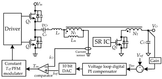
Figure 5.
Circuit structure of the prototype circuit.

Table 1.
Specification of the prototype circuit.
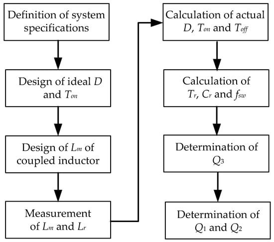
Figure 6.
Design flow chart.
3.1. Design of Ideal D and Ton
First, the ideal duty cycle is obtained as (69) and (70) without considering the leakage inductance Lr. Then, the ideal VCr(24V) and VCr(48V) can be obtained as (71) and (72). The ideal values of Ton are shown in (73) and (74).
3.2. Design of Ideal Lm of the Coupled Inductor
The turns ratio of the coupled inductor L and the maximum flux density Bmax are defined to be 2:1 and 0.1 T, respectively. Then, the turns of L can be designed according to the given information of Bmax and core material. Then, the ideal windings of L are calculated as (75) to (77). The ideal magnetizing inductance Lm is calculated in (78). However, the leakage inductance Lr is highly relative to its geometry structure. The value of Lr is measured after the coupled inductor L of the prototype is made.
3.3. Measurement of Lm and Lr
The coupled inductor L of the prototype is measured with an LCR meter, and the values of Lm and Lr are obtained as 18.2 μH and 1.9 μH, respectively. The values of D, Ton, and Toff can be recalculated according to [22] as (79) to (82).
3.4. Calculation of Actual D, Ton and Toff
The Ton, Toff, D, and the voltage gain can be reprensented as (79), (76), (81), and (82), respectively.
3.5. Determination of Tr, Cr and fsw
The current iLr can discharge and charge Coss1 and Coss2, respectively. To extend the effect of ZVS turn-on to light load as much as possible, it is better to design Toff to be Tr/4 so as to obtain iLr at its maximum point. The maximum frequency designed at 180 kHz with Cr as 4.45 μF and 5.06 μF for input voltages of 48 V and 24 V, respectively.
Finally, Cr is chosen to be a 4.7 μF MLCC. Then, fsw is recalculated to obtain 179 kHz and 155 kHz at input voltages of 24 V and 48 V, respectively.
3.6. Determination of Q3
Q3 is a synchronous rectifier, which always has a ZVS turn-on function without considering switching loss. The minimum rated voltage of Q3 can be expressed as (94). To reduce conduction loss, the AON6500 is adopted with drain-source resistance of 0.95 mΩ and a rated voltage of 30 V.
3.7. ZVS Operation of Q1 and Q2
The ZVS operation of Q1 and Q2 is needed to satisfy the condition in (95) when in state 5. From (96), it can be seen that more iLr can result in ZVS turn-on. However, the output capacitance of a MOSFET is nonlinear and varies with vds. Consequently, it is not easy to obtain an accurate result from calculations in (96) and (97).
Table 2 is the list of the key components in the prototype circuit.
Table 2.
Key components information of the prototype circuit.
4. Experimental Results
Figure 7 shows the experimental setup blocks of the system test.
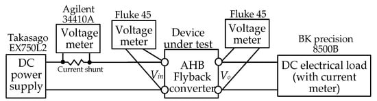
Figure 7.
Measurement setup of the system test.
Figure 8a shows the measured result of the conversion efficiency. The prototype can achieve better efficiency at lower input voltages and more load currents. This prototype circuit is based on COT control, so the controller increases Ton and reduces fsw as the load increases. When the input voltage decreases, Ton also increases. Figure 8b shows the frequency curve with variation of load current and input voltage. Since the previous calculation does not take the parasitic effect of individual components into consideration, the actual switching frequency is lower than the theoretical calculation result. The results of fsw at high input voltage and low input voltage at light load are 148 kHz and 129 kHz, respectively. Finally, the variation range Δfsw of fsw can be calculated as ±16.7%, which is much less than the results of ±95.4% in [1] and ±100% in [2], respectively.
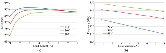
Figure 8.
Measured curves of conversion efficiency and switching frequency: (a) conversion efficiency; (b) switching frequency.
Figure 9 and Figure 10 show the measured waveforms of vgs1, vds1, vgs2, and vds2 for different input voltages of 24 V and 48 V at 10%, 50%, and 100% load, respectively. They show that higher input voltage induces more parasitic capacitance energy of the switch and lower iLr under the same load, so it is not easy to achieve the complete ZVS turn-on. However, the switches turned-on at the lowest vds still reduce the switching loss. As the load increases, iLr rises to expand the voltage range of ZVS turn-on. When the output load is more than 40% of the rated load, ZVS turn-on is also achieved at the high voltage input.
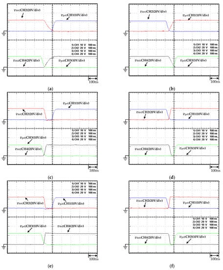
Figure 9.
Measured waveforms of vgs1, vds1, vgs2, and vds2 at input 24 V under (a) Q1 turned-on at 10% load; (b) Q1 turned-off at 10% load; (c) Q1 turned-on at half load; (d) Q1 turned-off at half load; (e) Q1 turned-on at full load; and (f) Q1 turned-off at full load.
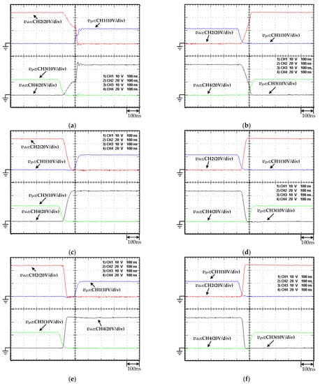
Figure 10.
Measured waveforms of vgs1, vds1, vgs2, and vds2 at input 48 V under (a) Q1 turned-on at 10% load; (b) Q1 turned-off at 10% load; (c) Q1 turned-on at half load; (d) Q1 turned-off at half load; (e) Q1 turned-on at full load; and (f) Q1 turned-off at full load.
Figure 11 and Figure 12 show the measured waveforms of vgs1, vgs2, vCr, and iLr for different input voltages of 24 V and 48 V at 10%, 20%, 50%, and 100% load, respectively. The variation of iLr and vCr at different input voltages is not significant. However, iLr and vCr increase significantly with the rising load.
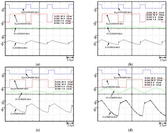
Figure 11.
Measured waveforms of vgs1, vgs2, vCr, and iCr at input 24 V under (a) 10% load; (b) 20% load; (c) half load; and (d) full load.
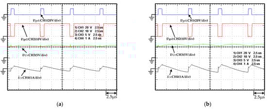
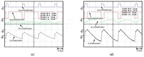
Figure 12.
Measured waveforms of vgs1, vgs2, vCr, and iCr at input 48 V under (a) 10% load; (b) 20% load; (c) half load; and (d) full load.
Figure 13 and Figure 14 show the waveforms of vgs1, vgs2, vds3, and iN2 for different input voltages of 24 V and 48 V at 10%, 20%, 50%, and 100% load, respectively. The more iN2 is, the higher vds3 becomes. This is the driving mechanism of MP6905 SR IC, which controls the conduction resistance of MOSFET Q3 at a fixed interval, so that vds3 remains at −32 mV.
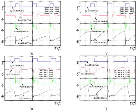
Figure 13.
Measured waveforms of vgs1, vgs2, vds3, and iN2 at input 24 V under (a) 10% load; (b) 20% load; (c) 50% load; and (d) 100% load.
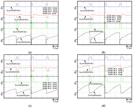
Figure 14.
Measured waveforms of vgs1, vgs2, vds3, and iN2 at input 48 V under (a) 10% load; (b) 20% load; (c) 50% load; and (d) 100% load.
Figure 15 shows the measurement results of the phase margin (PM) and gain margin (GM) under different load and different input voltage conditions, and the effect of increasing load on PM and GM is not significant under the same input voltage. Under the same load, the change of input voltage can cause the PM and GM to deteriorate. The detailed results are shown as Table 3. According to [34,35], the experimental results of GM of 6 dB and PM of 45° can make sure the closed-loop system is stable.
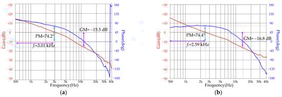
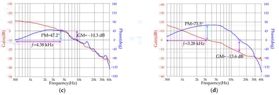
Figure 15.
Measured curves of gain margin and phase margin under (a) 10% load at input 24 V; (b) full load at input 24 V; (c) 10% load at input 48 V; and (d) full load at input 48 V.
Table 3.
Measured results of phase margin and gain margin.
Figure 16 shows the experimental results of the load transient response. vCF is the current reference of the inner current-loop controller. Vo(AC) and vCr(AC) are the ac coupled signals from Vo and vCr to enlarge the ripple waveforms, respectively. Due to the weak sampling rate and the memory depth of the oscilloscope, the waveforms are measured with significant glitch. The measured results show the close loop response is stable under load transient at different input voltages.
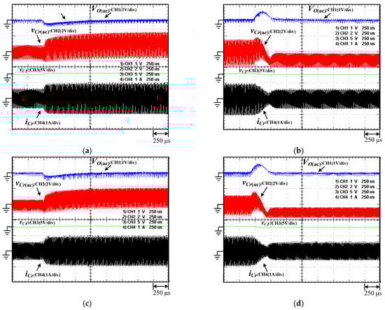
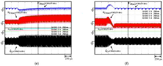
Figure 16.
Measured transient waveforms of Vo ripple, vCr ripple, vCF, and iCr: (a) from 50% to 100% load at 24 V input; (b) from 100% to 50% load at 24 V input; (c) from 50% to 100% load at 36 V input; (d) from 100% to 50% load at 36 V input; (e) from 50 to 100% load at 48 V input; and (f) From 100% to 50% load at 48 V input.
Table 4 shows the comparison of the proposed and other topologies. Figure 17 shows the photographs of the power stage of the proposed prototype, not showing the part of the controller. Q1~Q3 and SR IC are soldered to the PCB in an upside-down placement, and only the bottom of the components can be seen externally. There is a buck module to power the FPGA control board.
Table 4.
Comparison of the proposed method and other topologies.
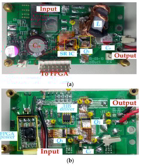
Figure 17.
Photographs of the proposed prototype (a) view of top side; and (b) view of bottom side.
5. Conclusions
This paper proposes an AHB flyback converter derived from a resonant high step-down converter. For applications with wide input voltage range, this circuit features the same low stress on all active switches as an LLC converter with fewer components and less frequency variation than an LLC converter. Compared to the ACF converter, the proposed AHB flyback has a similar wide input voltage range with ZVS turn-on, but lower voltage stress on all active switches. Finally, the system performance and stability are verified with the prototype circuit.
Funding
This research was supported by the Ministry of Science and Technology, Taiwan, under the Grant Number: MOST 109-2222-E-167-003-MY3.
Institutional Review Board Statement
Not applicable.
Informed Consent Statement
Not applicable.
Data Availability Statement
No new data were created or analyzed in this study. Data sharing is not applicable to this article.
Conflicts of Interest
The author declares no conflict of interest.
Abbreviations
| Symbol and Variable | Definition |
| Vin | Input voltage |
| VO | Output voltage |
| L | Main coupled inductor |
| Lm | Magnetizing inductor of main coupled inductor |
| Q1, Q2 | Main switch |
| Q3 | Synchronous Rectifier switch |
| CO | Output capacitor |
| Coss1, Coss2, Coss3 | Output capacitance of Q1, Q2, and Q3, respectively |
| Qrr3 | Reverse recovery charge of Q3 |
| Lr | Resonance inductor |
| Cr | Input capacitor |
| fsw | Switching frequency |
| Ts | Switching period |
| fsw(24V), fsw(48V) | Switching frequency at input voltages of 24 V and 48 V, respectively |
| D | Duty cycle |
| D(24V), D(48V) | Duty cycle at input voltages of 24 V and 48 V, respectively |
| Ton | Conduction time of Q1 |
| Ton(24V), Ton(48V) | Conduction time of Q1 at input voltages of 24 V and 48 V, respectively |
| Toff | Disconduction time of Q1 |
| iLm | Current of Lm |
| iN1, iN2 | Current of N1 and N2, respectively |
| iLr | Current of Lr |
| iLr(pk) | Peak current of Lr |
| ids1, ids2, ids3 | Drain-source current of Q1, Q2, and Q3, respectively |
| vds1, vds2, vds3 | Drain-source voltage of Q1, Q2, and Q3, respectively |
| iCr | Current of Cr |
| vCr | Voltage across Cr |
| Z1 | Impedance of resonant tank of Cr, Lm, and Lr |
| Z2 | Impedance of resonant tank of Cr, Coss1, Coss2, Lm, and Lr |
| Z3 | Impedance of resonant tank of Cr and Lr |
| Z4 | Impedance of resonant tank of Lr and Cds3 |
| ωr1 | Angular frequency of resonant tank of Cr, Lm, and Lr |
| ωr2 | Angular frequency of resonant tank of Cr, Coss1, Coss2, Lm, and Lr |
| ωr3 | Angular frequency of resonant tank of Cr and Lr |
| ωr4 | Angular frequency of resonant tank of Lr and Cds3 |
| Tr | Resonant period of Cr and Lr |
| fmax, fmin | Maximum and minimum of fsw, respectively |
| Δfsw | Variation rang of fsw |
| Ae | Magnetic cross sectional area of L |
| Le | Mean magnetic path length of L |
| Bmax | Maximum flux density of Lm |
| VCr | Average value of vCr |
| VCr(24V), VCr(48V) | Average value of vCr at input voltage 24 V and 48 V, respectively |
| vCF | Current reference of the inner current-loop controller |
| Vo(AC) | AC coupled signals of Vo |
| vCr(AC) | AC coupled signals of vCr |
| Vref, iref | Reference of the voltage loop compensator and the current loop, respectively |
| verr | Feedback error of the voltage loop |
References
- Beiranvand, R.; Rashidian, B.; Zolghadri, M.R.; HosseinAlavi, S.M. Using LLC resonant converter for designing wide-range voltage source. IEEE Trans. Ind. Electron. 2011, 58, 1746–1756. [Google Scholar] [CrossRef]
- Musavi, F.; Craciun, M.; Gautam, D.S.; Eberle, W.; Dunford, W.G. An LLC resonant DC–DC converter for wide output voltage range battery charging applications. IEEE Trans. Power Electron. 2013, 28, 5437–5445. [Google Scholar] [CrossRef]
- Lin, B.R.; Chen, K.Y. Hybrid LLC converter with wide range of zero-voltage switching and wide input voltage operation. Appl. Sci. 2020, 10, 8250. [Google Scholar] [CrossRef]
- Lin, B.R.; Liu, Y.C. Implementation of a wide input voltage resonant converter with voltage doubler rectifier topology. Electronics 2020, 9, 1931. [Google Scholar] [CrossRef]
- Lin, B.R.; Dai, C.X. Wide voltage resonant converter using a variable winding turns ratio. Electronics 2020, 9, 370. [Google Scholar] [CrossRef] [Green Version]
- Gu, Y.L.; Lu, Z.Y.; Hang, L.J.; Qian, Z.M.; Huang, G.S. Three-level LLC series resonant DC/DC converter. IEEE Trans. Power Electron. 2005, 20, 781–789. [Google Scholar] [CrossRef]
- Yuan, Y.S.; Mei, X.L. Five-level LLC resonant converter suitable for wide output voltage range. Electron. Lett. 2005, 54, 1187–1189. [Google Scholar] [CrossRef]
- Hu, H.B.; Fang, X.; Chen, F.; Shen, Z.J.; Batarseh, I. A modified high-efficiency LLC converter with two transformers for wide input-voltage range applications. IEEE Trans. Power Electron. 2013, 28, 1946–1960. [Google Scholar] [CrossRef]
- Shang, M.; Wang, H.Y. A voltage quadrupler rectifier based pulsewidth modulated LLC converter with wide output range. IEEE Tran. Ind. Appl. 2018, 54, 6159–6168. [Google Scholar] [CrossRef]
- Wang, H.Y.; Li, Z.Q. A PWM LLC type resonant converter adapted to wide output range in PEV charging applications. IEEE Trans. Power Electron. 2018, 33, 3791–3801. [Google Scholar] [CrossRef]
- Gu, L.; Liang, W.; Praglin, M.; Chakraborty, S.; Juan, R.D. A wide-input-range high-efficiency step-down power factor correction converter using a variable frequency multiplier technique. IEEE Trans. Power Electron. 2018, 33, 9399–9411. [Google Scholar] [CrossRef]
- Hwu, K.I.; Yau, Y.T.; Lee, L.L. Powering LED using high-efficiency SR flyback converter. IEEE Trans. Ind. Appl. 2011, 47, 376–386. [Google Scholar] [CrossRef]
- Alganidi, A.; Moschopoulos, G. A comparative study of two passive regenerative snubbers for flyback converters. In Proceedings of the Conference Record of the IEEE International Symposium on Circuits and Systems (ISCAS), Florence, Italy, 27–30 May 2018; pp. 1–4. [Google Scholar]
- Dzhunusbekov, E.; Orazbayev, S. A new passive lossless snubber. IEEE Trans. Power Electron. 2021, 36, 9263–9272. [Google Scholar] [CrossRef]
- Yau, Y.T.; Hung, T.L. Lossless snubber for GaN-based flyback converter with common mode noise consideration. IEEE Access 2022, 10, 56652–56667. [Google Scholar] [CrossRef]
- Yau, Y.T.; Jiang, W.Z.; Hwu, K.I. Light-load efficiency improvement for flyback converter based on hybrid clamp circuit. In Proceedings of the Conference Record of the IEEE International Conference on Industrial Technology (ICIT), Taipei, Taiwan, 14–17 March 2016; pp. 329–333. [Google Scholar]
- Xue, L.X.; Zhang, J. Highly efficient secondary-resonant active clamp flyback converter. IEEE Trans. Ind. Electron. 2011, 58, 1746–1756. [Google Scholar] [CrossRef]
- Perrin, R.; Quentin, N.; Allard, B.; Martin, C.; Ali, M. High-temperature GaN active-clamp flyback converter with resonant operation mode. IEEE Trans. Power Electron. 2016, 4, 1077–1085. [Google Scholar] [CrossRef]
- Huber, L.; Jovanović, M.M.; Song, H.B.; Xu, D.F.; Zhang, A.; Chang, C.C. Flyback converter with hybrid clamp. In Proceedings of the Conference Record of the IEEE Applied Power Electronics Conference and Exposition (APEC), Orlando, FL, USA, 19–23 March 2018; pp. 2098–2103. [Google Scholar]
- Xu, X.; Khambadkone, A.M.; Oruganti, R. An asymmetrical half bridge flyback converter with zero-voltage and zero-current switching. In Proceedings of the Conference Record of the Annual Conference of IEEE Industrial Electronics Society (IECON), Busan, Korea, 2–6 November 2004; pp. 767–772. [Google Scholar]
- Kim, H.S.; Jung, J.H.; Baek, J.W.; Kim, H.J. Analysis and design of a multioutput converter using asymmetrical PWM half-bridge flyback converter employing a parallel–series transformer. IEEE Trans. Ind. Electron. 2013, 60, 3115–3125. [Google Scholar]
- Seo, D.H.; Lee, O.J.; Lim, S.H.; Park, J.S. Asymmetrical PWM flyback converter. In Proceedings of the Conference Record of the IEEE Annual Power Electronics Specialists Conference (PESC), Galway, Ireland, 23–26 June 2000; pp. 848–852. [Google Scholar]
- Cho, J.S.; Kwon, J.G.; Han, S.Y. Asymmetrical ZVS PWM flyback converter with synchronous rectification for ink-jet printer. In Proceedings of the Conference Record of the IEEE Annual Power Electronics Specialists Conference (PESC), Jeju, Korea, 18–22 June 2006; pp. 1–7. [Google Scholar]
- Chen, T.M.; Chen, C.L. Characterization of asymmetrical half bridge flyback converter. In Proceedings of the Conference Record of the IEEE Annual Power Electronics Specialists Conference (PESC), Jeju, Korea, 18–22 June 2006; pp. 921–926. [Google Scholar]
- Chen, Y.F.; Nguyen, T.D.; Lin, J.Y.; Hsieh, Y.C.; Chiu, H.J. Hybrid-switching asymmetrical half-bridge flyback DC-DC converter. In Proceedings of the Conference Record of the IEEE International Conference on Industrial Technology (ICIT), Taipei, Taiwan, 14–17 March 2016; pp. 1313–1317. [Google Scholar]
- Lin, B.R.; Yang, C.C.; Wang, D. Analysis, design and implementation of an asymmetrical half-bridge converter. In Proceedings of the Conference Record of the IEEE International Conference on Industrial Technology (ICIT), Seville, Spain, 17–19 March 2015; pp. 1209–1214. [Google Scholar]
- Huber, L.; Jovanović, M.M. Analysis, design, and performance evaluation of asymmetrical half-bridge flyback converter for universal-line-voltage-range applications. In Proceedings of the Conference Record of the IEEE Applied Power Electronics Conference and Exposition (APEC), Tampa, FL, USA, 26–30 March 2017; pp. 2481–2487. [Google Scholar]
- Li, H.; Zhou, W.J.; Zhou, S.P.; Yi, X. Analysis and design of high frequency asymmetrical half bridge flyback converter. In Proceedings of the Conference Record of the IEEE International Conference on Electrical Machines and Systems (ICEMS), Wuhan, China, 17–20 October 2008; pp. 1902–1904. [Google Scholar]
- Jung, J.H. Feed-forward compensator of operating frequency for APWM HB flyback converter. IEEE Trans. Power Electron. 2012, 27, 211–223. [Google Scholar] [CrossRef]
- Medina-Garcia, A.; Schlenk, M.; Morales, D.P.; Rodriguez, N. Resonant hybrid flyback, a new topology for high density power adaptors. Electronics 2018, 7, 363. [Google Scholar] [CrossRef] [Green Version]
- Yau, Y.T.; Jiang, W.Z.; Hwu, K.I. Analysis and design of a high-step-down ratio resonant converter. IET Power Electron. 2016, 9, 864–873. [Google Scholar] [CrossRef]
- Hwu, K.I.; Wang, C.W.; Yau, Y.T. Enhancement of system stability based on PWFM. Electronics 2019, 8, 399. [Google Scholar] [CrossRef] [Green Version]
- Yau, Y.T. Asymmetrical half bridge flyback converter with constant off time control. In Proceedings of the Conference Record of the IEEE International Midwest Symposium on Circuits and Systems (MWSCAS), Online, 7–10 August 2022; pp. 1–4. [Google Scholar]
- Chuang, C.C.; Hua, C.C.; Huang, C.Y.; Jhou, L.K. Modeling a dual-mode controller design for a quasi-resonant flyback converter. Appl. Sci. 2019, 9, 1860. [Google Scholar] [CrossRef] [Green Version]
- Zang, H.J. Application Note of Modeling and Loop Compensation Design of Switching Mode Power Supplies. Available online: https://www.analog.com/media/en/technical-documentation/application-notes/an149fa.pdf (accessed on 1 January 2015).
Publisher’s Note: MDPI stays neutral with regard to jurisdictional claims in published maps and institutional affiliations. |
© 2022 by the author. Licensee MDPI, Basel, Switzerland. This article is an open access article distributed under the terms and conditions of the Creative Commons Attribution (CC BY) license (https://creativecommons.org/licenses/by/4.0/).