Article

A 2.4 GHz 20 W 8-Channel RF Source Module with Improved Channel Output Balance

1
Department of Electronic System Engineering, Hanyang University, Ansan 15588, Korea
2
Department of Electrical and Electronic Engineering, Hanyang University, Ansan 15588, Korea
*
Author to whom correspondence should be addressed.
Appl. Sci. 2021, 11(16), 7491; https://doi.org/10.3390/app11167491
Submission received: 20 May 2021 / Revised: 7 August 2021 / Accepted: 11 August 2021 / Published: 15 August 2021
(This article belongs to the Special Issue Radio-Frequency High Power Amplifier)

Abstract

:

Featured Application

RF source for plasma generator.

Abstract

This paper presents a 2.4 GHz 20 W 8-channel radio frequency (RF) source module with improved channel output balance. The proposed RF source module is composed of an RF source generation/DC control part, a power amplification part, and a power dividing part. A 2-stage power amplifier (PA) is combined with gallium nitride high-electron-mobility transistors, including a 25 W transistor and 2-way combined 120 W transistors as the drive and main PA, respectively. In addition, a structure was applied to improve the channel output balance compared to that of the previous module, and the differences of the phase and magnitude of the output power between channels are alleviated within 0.35° and 0.18 dB, respectively. A water jacket was implemented under the drive and main PAs for liquid cooling; however, unlike in the previous work, it was designed by optimizing the size of the water jacket and reducing unnecessary materials using a brazing process. The output power at each channel was 43 dBm, and the drain efficiency was more than 50% at 2.4 GHz. The total module size was 244 mm × 247.4 mm × 30 mm, and its volume was reduced by approximately 58.4% compared to that of the previous module.

1. Introduction

RF source modules for plasma generators have been used as a magnetron type in the sub-GHz frequency band, but recently this type of module has been developed by using a solid-state power amplifier (SSPA) in the 2.4 GHz industrial–scientific–medical (ISM) band [1,2,3,4,5,6]. To produce high-quality wafers in the semiconductor process, area coverage, uniformity and reliability during plasma generation should be considered [7,8]. Until now, plasma RF sources have had low area coverage, because they consisted of one channel with high output power [9,10]. In addition, there was a problem in that the density of the center and that of the periphery are not uniform, which degrades reliability. Furthermore, it was difficult to improve the drain efficiency due to the high-level output power. Although various attempts have been made to improve plasma density by configuring multi-channels, there was a problem in that the size, weight, and cost of the entire system increased because individual RF sources were required as much as the number of plasma sources [4,5]. For this reason, an 8-channel RF source module was previously presented that focused on area coverage, uniformity, and drain efficiency [11]. Although improvement of the drain efficiency was confirmed in the previous module, the uniformity problem could not be completely solved due to the difference in transistor performance as a result of a 2-stage power amplifier (PA) being applied to each channel. Moreover, due to there being many devices, such as voltage gain amplifiers (VGAs) and relays to control the transistors, the size of the module including the DC control part was inevitably increased.
Therefore, in this paper, a 2.4 GHz 20 W 8-channel RF source module with improved channel output balance is proposed to solve the aforementioned problems. The power amplification part is simply constructed to a single 2-stage PA that has a high-level output power to improve the channel output balance. The output terminal consists of 8-channel as previously mentioned, but it is implemented with a 3-section of 2-way Wilkinson divider, not a commercial 2-way divider, to minimize the magnitude and phase difference between channels. Additionally, the channel spacing was reduced to 3.2 cm to improve the uniformity. In addition, to alleviate performance degradation due to high-level output power characteristic, a water jacket is optimized to improve the drain efficiency and the module size. The remainder of this paper is organized as follows. Section 2 describes the proposed RF source module, which is classified into three parts. The measurement results of the proposed RF source module are presented in Section 3. Finally, concluding remarks are provided in Section 4.

2. Materials and Methods

The proposed RF source module is classified into three parts: an RF source generation/DC control part, a power amplification part, and a power dividing part, as shown in Figure 1.

2.1. RF Source Generation/DC Control Part

The RF source generation/DC control part provides DC bias to ensure the safe operation of the proposed RF source module and generates an initial RF source delivered to the power amplification part. At the first step, a voltage-controlled oscillator (VCO), CVCO55CC-2328-2536 (Crystek Corporation, Fort Myers, USA) generates an initial RF source that has a specific frequency controlled by the DC control voltage without a signal generator. Then, a voltage gain amplifier (VGA), MAX2057ETX+ (Maxim Integrated, San Jose, USA), is used to provide insufficient gain between the VCO and source PA. This is also tuned by the DC control voltage. To control the frequency of the VCO and the gain of the VGA, trimmer resistors, 3214W-1-204E (Bourns, Altadena, USA), are used. Subsequently, the source PA, ACPM-5040 (Avago Technologies, San Jose, USA), amplifies the delivered power from the VGA up to 30 dBm to transmit it to the power amplification part. The DC bias of the source PA uses VSRC_EN = 2.6 V and VSRC_CC = 5 V.
Six external DC biases are required to operate the proposed RF source module, as shown in Table 1. The module requires 30 V of the main DC bias, called VSUPPLY. The rest of the DC bias is used as the control bit for the proposed module operation as described in Table 2. This is because it prevents the drive and main PAs from burning out through sequential on/off. Gallium nitride high electron mobility transistor (GaN HEMT) devices normally have an on-state characteristic. If a drain bias is applied without closing the drain–source channel, excessive current flows through the channel, causing damage to the transistor. The process of turning off is in the reverse order of the operating sequence. A solid-state relay (SSR), CMX60D20 (Crydom, Mansfield, USA), supplies a drain bias for the drive and main PAs. The other relays, 8L01-05-111 (Coto Technology, North Kingstown, RI, USA) for SPST and 8L61-05-111 (Coto Technology, North Kingstown, USA) for SPDT, act as switches to turn the other active devices on or off. A negative charge pump, MAX868EUB (Maxim Integrated, San Jose, USA), generates a negative DC bias to maintain the off state of the drive and main PAs. Low dropout regulators (LDOs), TPS54560DDAR (Texas Instruments, Dallas, USA) and TPS7A7001DDAR (Texas Instruments, Dallas, USA), convert high-level voltage to low-level voltage to supply the proper DC bias to the components. A printed circuit board (PCB) for the RF source generation/DC control part was designed on 4-layer FR-4.
  • Sequence 1 (off state): When 30 V of the main DC bias, VSUPPLY, is applied, it is supplied to the SSR and converted from 30 V to 5 V using a low dropout regulator (LDO). Then, it is supplied to the remaining components in the RF source generation/DC control part. In contrast, some of the voltages are converted to negative voltages through the negative charge pump to maintain off state.
  • Sequence 2 (ideal state #1): When VSSR_CTRL becomes high, the SSR is activated to supply 30 V at the drain of the drive and the main PAs.
  • Sequence 3 (ideal state #2): When VMAIN_ CTRL and VDRV_ CTRL become high, the gate bias of the drive and main PAs is changed from –5 V to –2.7 V to activate these components.
  • Sequence 4 (power emission): When VSRC_ CTRL and VRF_ CTRL become high, the proposed RF source module generates 20 W output power at each channel.

2.2. Power Amplification Part

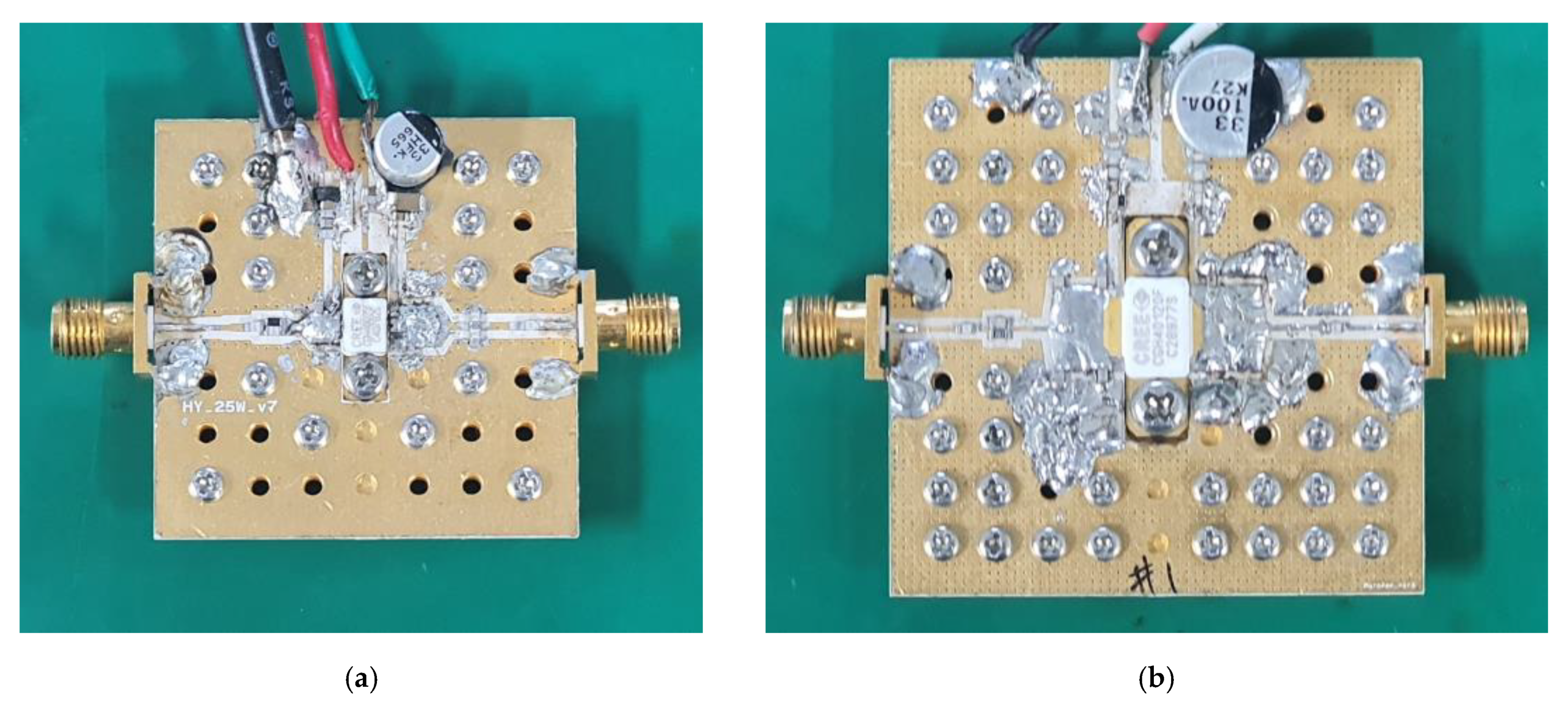
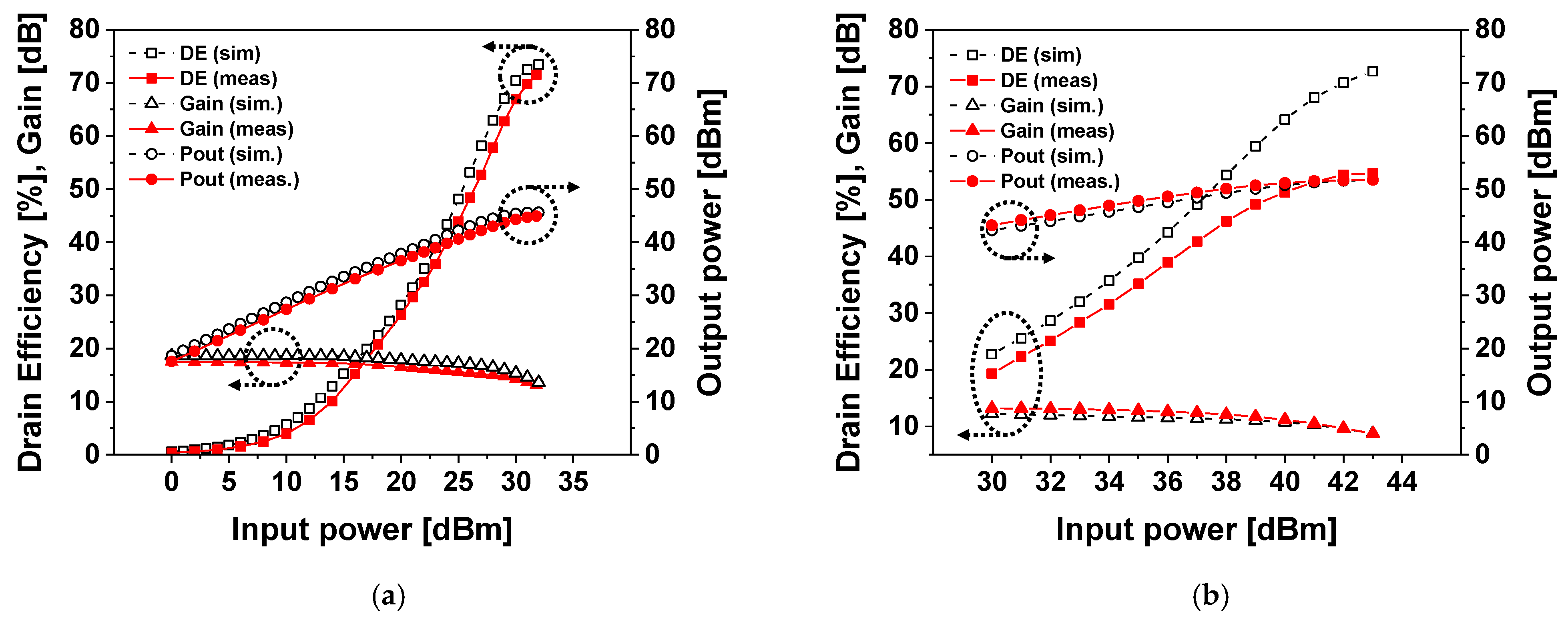
The delivered power from the RF source generation/DC control part is amplified over 53 dBm passing through the power amplification part. In the previous module, the power amplification part was implemented using gallium arsenide and GaN devices as a 2-stage PA and applied to each channel. In the proposed module, however, two types of GaN HEMT packaged transistors were used to implement a single 2-stage PA. Therefore, the number of transistors used is much smaller than that of the previous module; thus, this module has an advantage in terms of cost and DC control part size. The 2-stage PA consisted of a 25 W transistor, CGH40025F, for the drive PA and 2-way combined 120 W transistors, CGH40120F, for the main PA. To verify the performance of each transistor, test units were manufactured as shown in Figure 2. The DC bias of the drive and the main PA used VMAIN_GG = VDRV_GG = −2.7 V and VMAIN_DD = VDRV_DD = 30 V, respectively. The measurement proceeded with continuous wave (CW) under natural convection at a room temperature of 25 °C. Figure 3a shows the measured RF characteristics of the drive PA test unit. The measurement results used swept input power from 0 to 33 dBm at 2.4 GHz. An output power of more than 40 dBm was achieved with more than 70% drain efficiency. Figure 3b shows the measured RF characteristics of the main PA test unit. Using a gain block, the input power was swept from 30 dBm to 43 dBm at 2.4 GHz. Output power of up to 50 dBm was achieved with a drain efficiency of over 50%. From the measurement results, it was confirmed that sufficient system target performance could be secured.
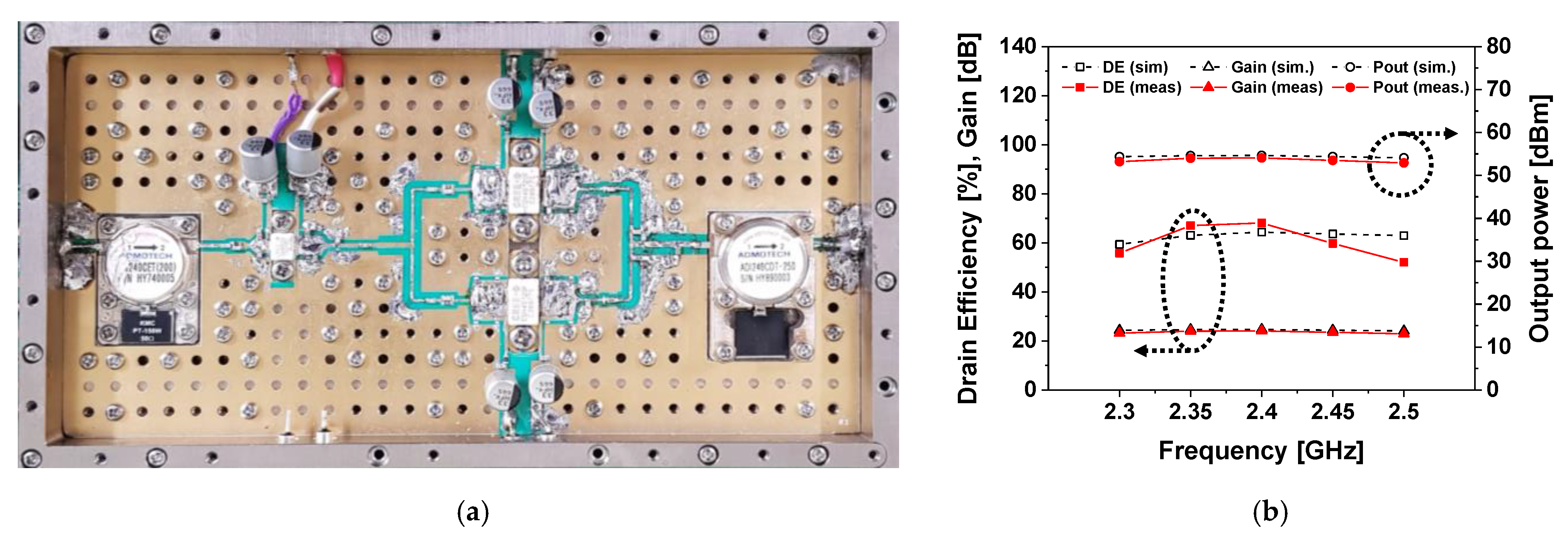
Using the above two types of transistors, a 2-stage PA test unit was fabricated, as shown in Figure 4a. Isolators, ADI240CET, were used at the input/output terminal of the 2-stage PA to avoid damage to the power amplification part caused by the reflected power in case of a mismatch. The PCB used for the power amplification part was a RT/duroid® 6010.LM (Rogers Corporation, Chandler, USA). The 2-stage PA was designed considering stability to ensure reliability. The stability is determined by Rollet’s factor, K, using network scattering parameters [12]. The stability factor of K is required to be larger than 1 at least to prevent oscillation; thus, it was confirmed that is K > 1 in the design and measurement. Moreover, the negative resistance was checked whether it existed at the input and output nodes or not. The DC bias of the drive and the main PA used VMAIN_GG = VDRV_GG = –2.7 V and VMAIN_DD = VDRV_DD = 30 V, respectively. As the measurement of the 2-stage PA was fabricated as a test unit, liquid cooling was not available, so it proceeded under a duty cycle of 10% pulsed wave. Figure 4b shows the measurement results. The output power reached over 53 dBm at 2.4 GHz and the adjacent frequency. The average value of the measured gain was 23 dB, and an average drain efficiency of over 50% was achieved.
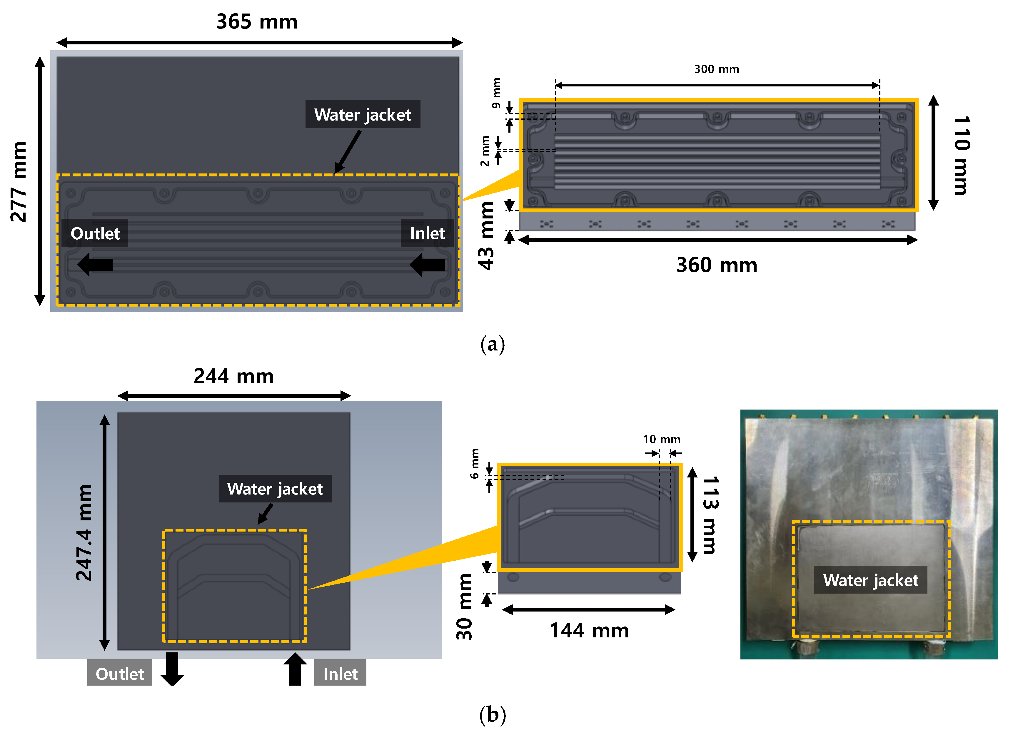
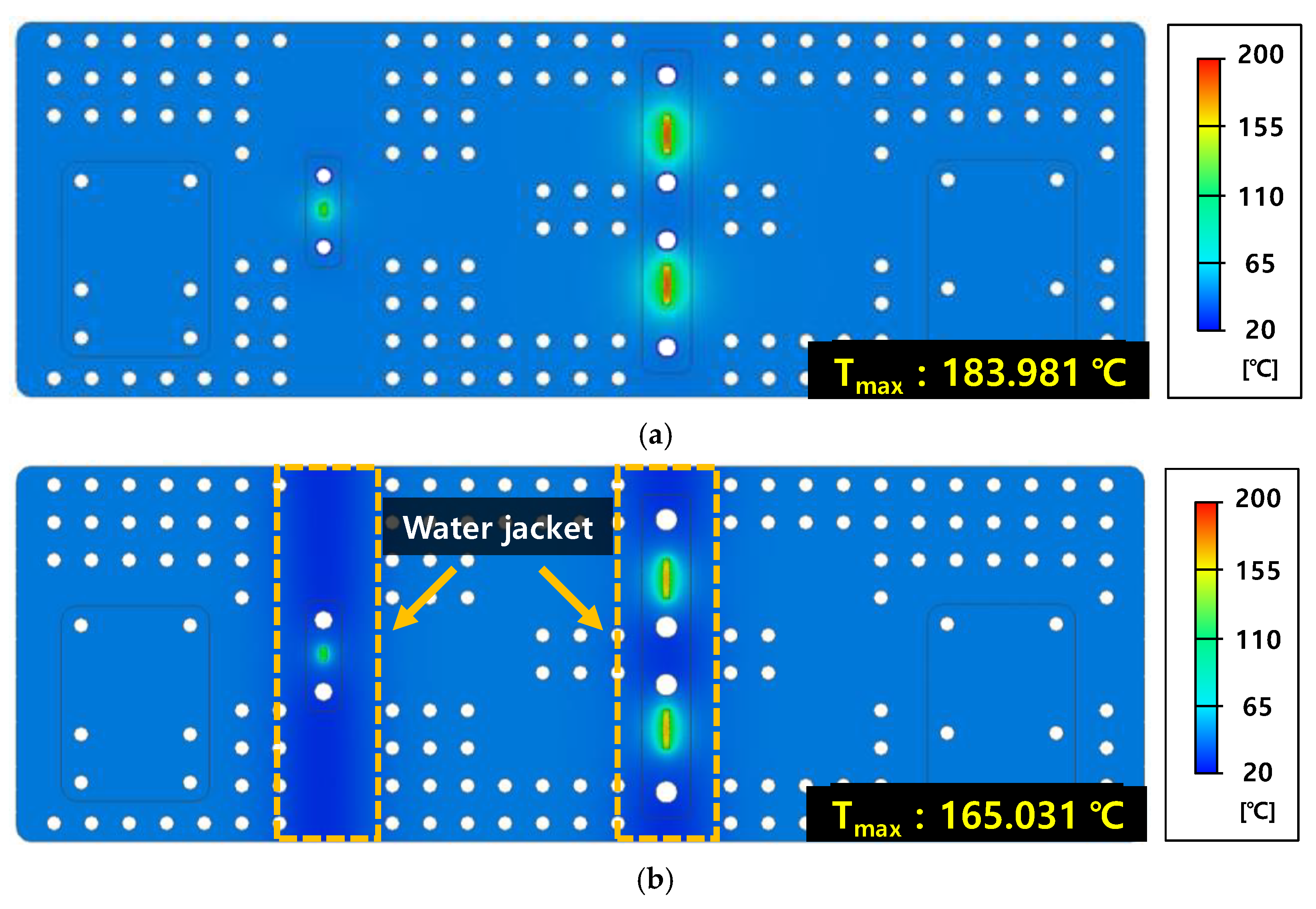
GaN-based high-power amplifiers have the advantage of high-power density, but they have a disadvantage of a high amount of heat density as well. Therefore, burnout or performance degradation, such as drain efficiency, can occur without a proper cooling system [13,14]. Therefore, it was required to consider thermal management when designing the power amplification part [15,16]. The previous module was implemented with a large water jacket, and the surrounding area was waterproofed using plate silicon and screws, as shown in Figure 5a. This method had a problem in that the module size increased because coolant can be distributed throughout the power amplification part. In addition, because the actual coolant path was not located just under the main PA where heat was intensively spread, the proposed module attempted to implement a water jacket using a more efficient method than the previous module. Figure 5b shows photographs of the proposed module, which implements a water jacket using a brazing process. The water jacket size was reduced through intensive cooling just below the heat source, and a brazing process was used to waterproof the joints of the bottom cover without additional materials [17,18]. For this reason, the module thickness was reduced by 13 mm compared to the previous module. Furthermore, while the size of the water jacket has been reduced, the cooling capacity is still good enough in the previous module. To prove the cooling capacity, thermal simulation was conducted based on the power amplification part. Thermal simulation considered the cases both with and without a water jacket. In the proposed module, the water jacket was located directly under the heat source, and the heat amount was set based on 25 W for the drive PA and 200 W for the main PAs. The coolant circulated with a temperature of 25 °C and a velocity of 0.1 m/s. The bottom temperature was set to 45 °C. Figure 6a,b show both without and with water jacket implementation in the proposed module, respectively. When looking at the operating temperature of the proposed module, the operating temperature presented an alleviation effect of approximately 19 °C according to whether water jacket implementation was carried out. The simulation results suggest the importance of the water jacket implementation, as well as of the optimized water jacket structure of the proposed module.

2.3. Power Dividing Part

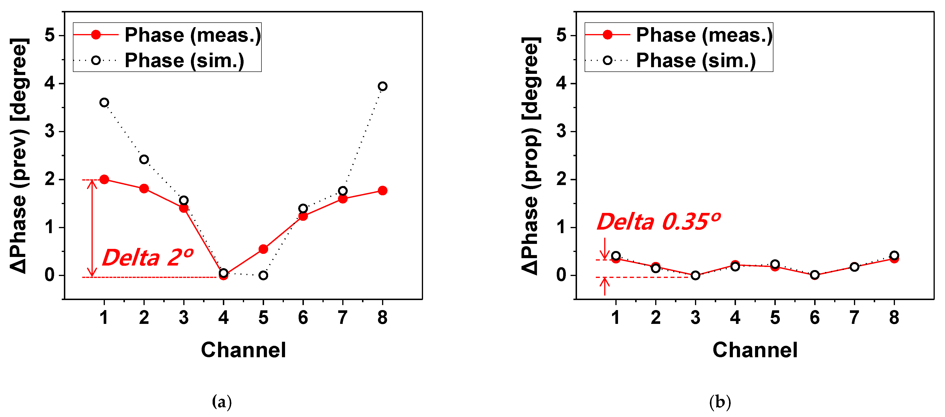
In the previous module, 2-way commercial dividers, GP2Y+, with transmission lines on FR-4 were used to design an 8-channel structure. It was also a method for uniform distribution between channels, but it could not predict the error between commercial components because the power divider was not its own design. Therefore, the power dividing part has been constructed with eight channels by combining three sections of the 2-way Wilkinson divider as shown in Figure 7 [19,20,21]. Characteristic impedance ( Z 0 ) of each port is based on 50 Ohm, and that of the dividing line is Z 0 2 . The length of the dividing line should be λ / 4 . The shunt resistor is used as 2 Z 0 ; in this case, 100 Ohm resistors were used. Important parameters during the multi-channel design of a plasma source include the phase and magnitude balance among channels that maintain the uniformity of the plasma generation. In the previous module, the channel spacing was 4.25 cm, but in the proposed module, the channel spacing was further reduced up to 3.2 cm, considering the cables to be connected to each channel. Moreover, the proposed RF source module considered detailed EM analysis to solve discontinuity at the intersection of the transmission lines from the beginning of the Wilkinson divider design on the Rogers RT/duroid® 6010.LM. To verify the output channel balance, each channel was measured from the network analyzer, ZVA 50, and the other channels were connected to 50 Ohm terminations. The measurement was based on an input power of 0 dBm. In the previous module, the phase difference occurred up to 2° from the center to the outer channel as shown in Figure 8a. In contrast, the proposed module proves that a phase difference within 0.35° can be achieved as shown in Figure 8b; thus, it was confirmed that the phase difference was reduced more than in the previous module. The difference in magnitude of the output power between the channels will be explained in Section 3.

3. Measurement Results

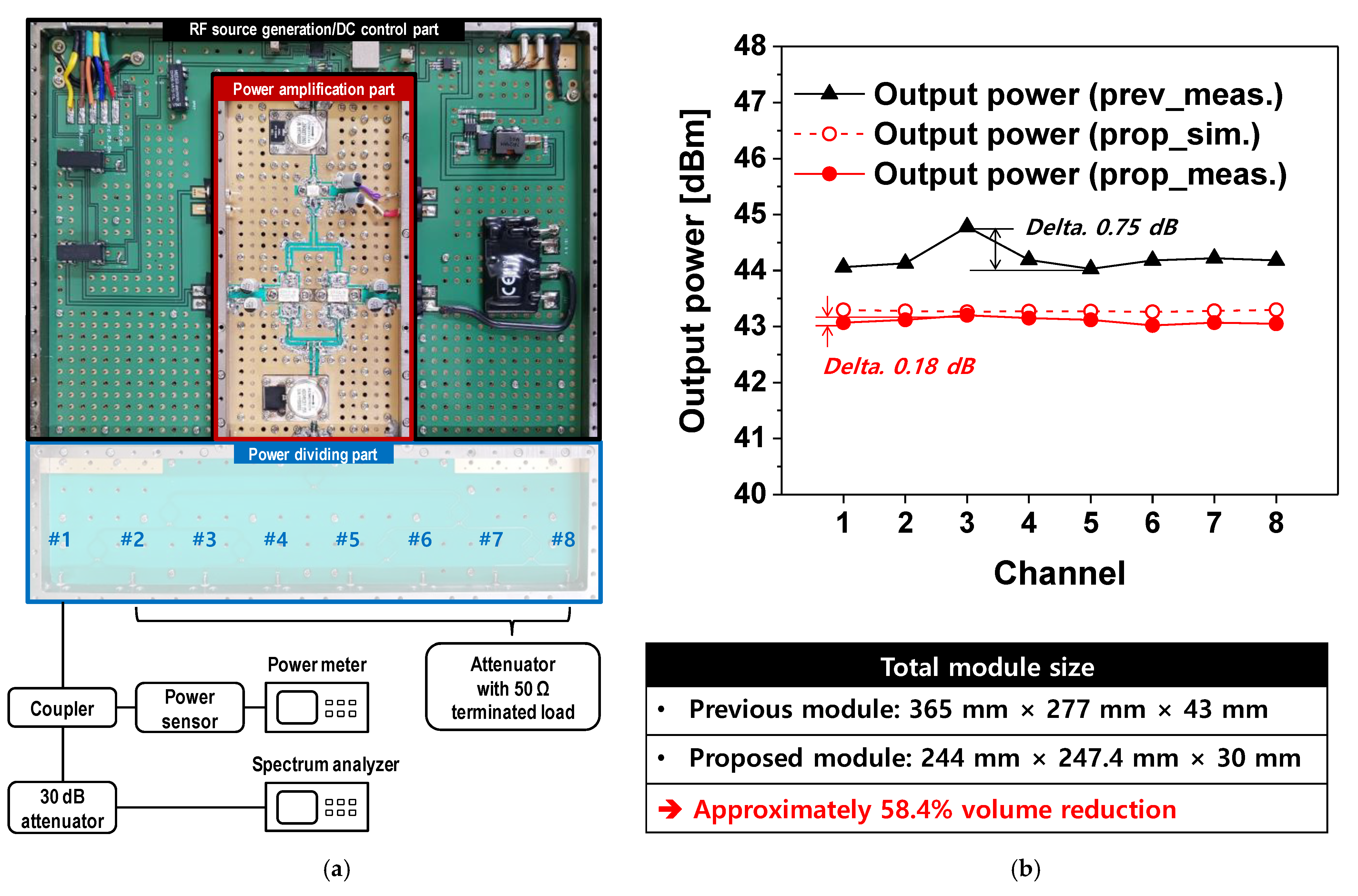
The proposed RF source module was implemented in an aluminum body as shown in Figure 9a. The total module size was 244 mm × 247.4 mm × 30 mm in width, length, and height, respectively. Each part was divided into 5 mm partition walls to prevent interference with between sections. As preparation before the measurement, seven of the eight channels were terminated with attenuators using 50 Ohm termination, and the remaining channel was connected to measurement setup. The measurements were performed by rotating each channel under the same conditions. The measurement setup consisted of E4417A (Keysight Technologies, Santa Rosa, USA) as a power meter, E9323A (Keysight Technologies, Santa Rosa, USA) as a power sensor, E4404B (Keysight Technologies, Santa Rosa, USA) as a spectrum analyzer, N5767A, E36312A, and E3632A (Keysight Technologies) as a DC supply, and Exos-2.5 (Koolance, Auburn, USA) as a liquid circulator. The measurement was performed with the top plate of the module covered, and coolant was circulated at a room temperature of 25 °C. The details of the measurement results are presented in Figure 9b. As for the output power, it can be confirmed that the target performance was achieved by securing an average of 43 dBm (20 W) for each channel. Moreover, in the previous module, there was a 0.75 dB difference in the output power between channels. In the proposed module, however, the difference of the output power was reduced to 0.18 dB; thus, it was confirmed that the channel output balance was improved. Furthermore, the proposed module has a volume 53.3% lower than that of the previous module.
In Table 3, the RF performance of the proposed RF source module is compared with that of the conventional research on plasma generator applications. In the conventional 1-channel application, the module has been manufactured as a pallet amplifier [9,10] or just a PA test unit [22]. The high-level output power can be presented as an advantage of the conventional 1-channel application, but the output power level of the proposed module can be further increased if it is replaced with a high-power transistor. In contrast, in the conventional multi-channel application, a method that combined several 1-channel modules was presented [4,5,23], but only the previous module implemented 8-channel operation by itself [11]. As the conventional modules are implemented by connecting multiple transistors or PA modules, the channel output balance may be different from that of the proposed module; however, the operation of the proposed module can achieve uniformity, high area coverage, and reliability. Further work could improve the module to be stackable to configure more output channels, which would allow it to cover a wider area under stable conditions.

4. Conclusions

A 2.4 GHz 20 W 8-channel RF source module with improved channel output balance for plasma generator applications is proposed. To equalize the variability between channels when the impedance of the output terminal changes due to plasma generation, a method of distributing eight channels from the high-power amplifier was applied. The channel spacing was also reduced to less than 4 cm to further improve uniformity, and the overall module size was reduced by 58.4% by simplifying the circuit configuration compared to that of the previous module. In addition, a Wilkinson divider was designed to reduce the phase and magnitude difference between channels, and the results are presented. Through the brazing process, water jacket implementation was optimized, and the module was further reduced in size and weight. The RF measurement shows that the output power was 20 W for each channel, and the drain efficiency was greater than 50%. This paper demonstrates that the use of a multi-channel RF source can be a promising design method to improve the channel output balance for plasma generator applications.

Author Contributions

Conceptualization, formal analysis, investigation, and resources, H.N. and J.K.; methodology, software, validation, data curation, writing—original draft preparation, writing—review and editing, and visualization, H.N., T.K., T.S. and S.B.; supervision, project administration, and funding acquisition, J.K. All authors have read and agreed to the published version of the manuscript.

Funding

This work was supported in part by the fourth BK21 Program through the National Research Foundation of Korea within the Ministry of Education, and in part by the National Research Foundation of Korea (NRF) grant funded by the Korea government (Ministry of Science).

Institutional Review Board Statement

Not applicable.

Informed Consent Statement

Not applicable.

Data Availability Statement

Not applicable.

Conflicts of Interest

The authors declare no conflict of interest.

References

  1. Petreus, D.; Grama, A.; Cadar, S.; Plaian, E.; Rusu, A. Design of a plasma generator based on E power amplifier and impedance matching. In Proceedings of the 2010 12th International Conference on Optimization of Electrical and Electronic Equipment, Basov, Romania, 20–22 May 2010; pp. 1317–1322. [Google Scholar]
  2. Miotk, R.; Jasinski, M.; Mizeraczyk, J. Optimization of microwave power transfer from electric field to the plasma inside an microwave 915 MHz plasma source. In Proceedings of the 2016 International Conference on Actual Problems of Electron Devices Engineering (APEDE), Saratov, Russia, 22–23 September 2016; pp. 1–8. [Google Scholar]
  3. Miotk, R.; Jasinski, M.; Mizeraczyk, J. Improvement of Energy Transfer in a Cavity-Type 915-MHz Microwave Plasma Source. IEEE Trans. Microw. Theory Tech. 2017, 66, 711–716. [Google Scholar] [CrossRef]
  4. Latrasse, L.; Radoiu, M.; Lo, J.; Guillot, P. 2.45-GHz microwave plasma sources using solid-state microwave generators. Collisional-type plasma source. J. Microw. Power Electromagn. Energy 2017, 51, 43–58. [Google Scholar] [CrossRef]
  5. Latrasse, L.; Radoiu, M.; Lo, J.; Guillot, P. 2.45-GHz microwave plasma sources using solid-state microwave generators. ECR-type plasma source. J. Microw. Power Electromagn. Energy 2017, 50, 308–321. [Google Scholar] [CrossRef]
  6. Latrasse, L.; Marilena, R.; Thomas, N.; Olivier, A. Self-matching plasma sources using 2.45 GHz solid-state generators: Microwave design and operating performance. J. Microw. Power Electromag. Energy 2017, 51, 237–258. [Google Scholar] [CrossRef]
  7. Chen, F.F.; Chang, J.P. Lecture Notes on Principles of Plasma Processing; Springer Science and Business Media: New York, NY, USA, 2003; pp. 25–30. [Google Scholar]
  8. Wu, R.; Benqing, G.; Zhenghui, X.; Weiming, L. The study of the RF field in a plasma reactor. In Proceedings of the Cross Strait Quad-Regional Radio Science and Wireless Technology Conference (CSQRWC) 2012, New Taipei City, Taiwan, 23–27 July 2012; pp. 191–194. [Google Scholar]
  9. RFM245-10, RFHIC Corp., Anyang, Republic of Korea.
  10. RCP25400-20L, RFHIC Corp., Anyang, Republic of Korea.
  11. Hyosung, N.; Taejoo, S.; Junghyun, K. A 2.4 GHz 20 W 8-channel RF Source Module with Solid-State Power Amplifiers for Plasma Generators. Electronics 2020, 9, 1378. [Google Scholar]
  12. Gonzalez, G. Microwave Transistor Amplifiers: Analysis and Design, 2nd ed.; Prentice Hall: Upper Saddle River, NJ, USA, 1997; pp. 217–227. [Google Scholar]
  13. Schefter, M.; Ardavan, M. A comparison of GaN VS GaAs system performance. Microw. J. 2019, 29, 17–22. [Google Scholar]
  14. Prejs, A.; Wood, S.; Pengelly, R.; Pribble, W. Thermal analysis and its application to high power GaN HEMT amplifiers. In Proceedings of the 2009 IEEE MTT-S International Symposium Digest, Boston, MA, USA, 7–12 June 2009; pp. 917–920. [Google Scholar]
  15. Yuxiang, L.; Chao, C.; Ruixiang, Y.; Yawen, O. Review: Special brazing and soldering. J. Manuf. Process. 2020, 60, 608–635. [Google Scholar]
  16. Ashutosh, S.; Seunghyun, L.; Hyungoh, B.; Youngsik, S.; Jaepil, J. Effect of Various Factors on the Brazed Joint Properties in Al Brazing Technology. J. Weld. Join. 2016, 34, 30–35. [Google Scholar]
  17. Xingcun, C.T. Advanced Materials for Thermal Management of Electronic Packaging; Springer Science & Business Media: Berlin, Germany, 2011. [Google Scholar]
  18. Ting, K.; Yuxin, Y.; Yungcong, J.; Yanmei, K.; Binbin, J. Enhanced Thermal Management of GaN Power Amplifier Electronics with Micro-Pin Fin Heat Sinks. Electronics 2020, 9, 1778. [Google Scholar]
  19. Pozar, D.M. Microwave Engineering, 4th ed.; Wiley: Hoboken, NJ, USA, 2012; pp. 564–570. [Google Scholar]
  20. Wilkinson, E.J. An N-Way Hybrid Power Divider. IRE Transact. Microw. Theory Techn. 1960, 8, 116–118. [Google Scholar] [CrossRef]
  21. Altaf, A.; Xi, C.; Dilshad, U.; Miao, J. Design of compact C-band one into eight-way equal Wilkinson Power Divider. In Proceedings of the 2019 International Conference on Microwave and Millimeter Wave Technology (ICMMT), Guangzhou, China, 19–22 May 2019; pp. 1–3. [Google Scholar]
  22. Bansleben, C.; Heinrich, W. Compact high-power high efficiency microwave generator with differential outputs. In Proceedings of the 2014 44th European Microwave Conference, Rome, Italy, 6–9 October 2014; pp. 723–726. [Google Scholar]
  23. Korpas, P.; Gryglewski, D.; Wojtasiak, W.; Gwarek, W. A Computer-controlled System of High-power Microwave Sources. Int. J. Electron. Telecommun. 2011, 57, 121–126. [Google Scholar] [CrossRef]
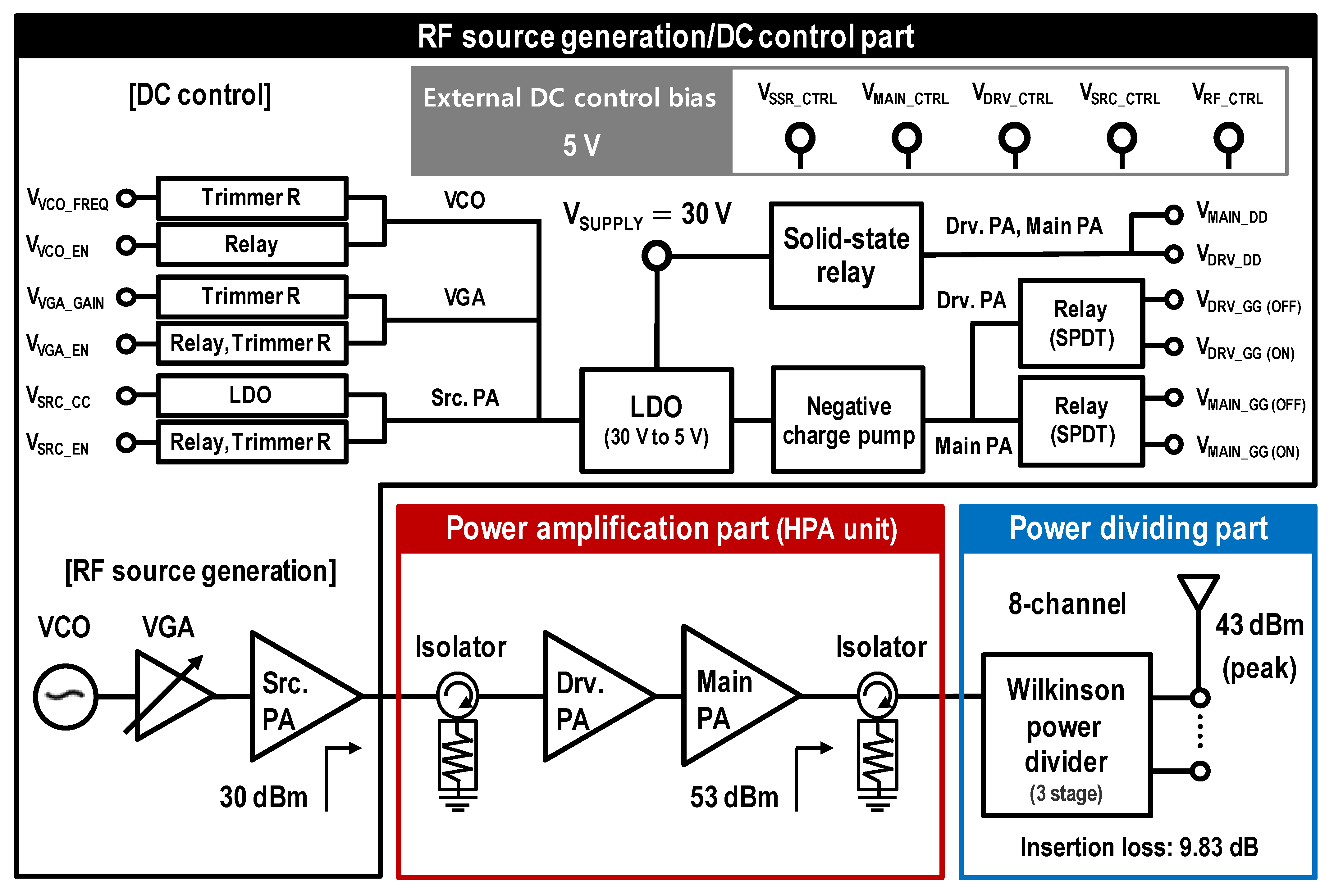
Figure 1. Block diagram of the proposed RF source module.
Applsci 11 07491 g001
Figure 2. Photographs of (a) the drive and (b) the main PA test unit.
Applsci 11 07491 g002
Figure 3. Simulated and measured RF characteristic of (a) the drive and (b) the main PA test unit.
Applsci 11 07491 g003
Figure 4. The 2-stage PA test unit: (a) a photograph; (b) RF characteristic with a duty cycle of 10%.
Applsci 11 07491 g004
Figure 5. System-level packaging with liquid cooling: (a) a 3D model of the previous module; (b) a 3D model and photograph of the proposed module using brazing process.
Applsci 11 07491 g005
Figure 6. Thermal simulation results: the proposed module (a) without and (b) with water jacket implementation.
Applsci 11 07491 g006
Figure 7. Photograph of the power dividing part using Wilkinson divider.
Applsci 11 07491 g007
Figure 8. Simulation and measurement results of the phase difference between channels: (a) in the previous module, (b) in the proposed module.
Applsci 11 07491 g008
Figure 9. (a) Photograph of the proposed RF source module with measurement setup; (b) measurement results of each channel.
Applsci 11 07491 g009
Table 1. Description of the external DC biases.
DC biasDC LevelDescription
VSUPPLY30 VMain DC source
VSSR_CTRLhigh (5 V)
or
low (0 V)
Control bit for the drain bias of the drive and main PAs
VMAIN_CTRLControl bit for the main PAs on/off
VDRV_CTRLControl bit for the drive PA on/off
VSRC_CTRLControl bit for the source PA on/off
VRF_CTRLControl bit for the VCO and the VGA on/off
Table 2. Operating sequence for the proposed RF source module.
SequenceVSSR_CTRLVMAIN_CTRLVDRV_CTRLVSRC_CTRLVRF_CTRLDescription
1LLLLLoff state
2HLLLLideal state #1
3HHHLLideal state #2
4HHHHHpower emission
Table 3. Comparison with 2.4 GHz ISM band RF sources for plasma generator applications.
Ref.Freq. (GHz)Output Power
Per
Channel (W)
Gain (dB)Drain
Efficiency
(%)
Channel
Configuration
CoolingSize
(W × L × H, mm3)
[4]2.45200--1 × NNone-
[5]2.45200--1 × NNone-
[9]2.45100-371None290 × 150 × 92
[10]2.4540013.8631None106 × 42.8 × 6.8
[22]2.457-471None36 × 36
[23]2.4520025-4None-
[11]
(prev. work)
2.4204052.58Liquid365 × 277 × 43
This work2.4202352.98Liquid244 × 247.4 × 30
Publisher’s Note: MDPI stays neutral with regard to jurisdictional claims in published maps and institutional affiliations.