1. Introduction
Single-phase AC-DC-AC converters with the same input/output frequencies can be found in multi-electric aircraft [
1], such as power interface units, standby power supplies, uninterruptible power supplier, etc. Large DC-link energy storage capacitors are usually used to adsorb pulsating power, which is harmful to the system, but the presence of the large electrolytic capacitor will lead to larger volume, heavier weight, and higher price [
2]. So, a great deal of research is devoted to reducing DC-link capacitor size and mitigating second-order power in the single-phase converter.
At present, non-electrolytic capacitive methods can be divided into two categories: active methods and passive methods [
3]. The main idea of the passive methods is to use passive components or passive networks instead of large electrolytic capacitors for energy storage. The simplest passive method is to replace the large electrolytic capacitor with multiple small-capacity non-electrolytic capacitors (such as film capacitors) in parallel, but its obvious disadvantages such as low withstand voltage, large volume, and high price limit its practical applications. In [
4,
5,
6,
7,
8], a resonance unit is used to replace the traditional DC energy storage unit, eliminating large-capacity energy storage components, while also realizing soft-switching, and the dynamic performance of the system is also improved. However, due to the shortcomings of the resonant unit itself, the circuit will generate higher voltage and current stress, and the conduction loss will also increase. In addition, this passive method also has the disadvantages of large volume and heavy weight.
The active methods mainly can be grouped into reducing or transferring the instantaneous power difference. Some control strategies are proposed in [
9,
10]. The instantaneous power difference between AC and DC sides is narrowed by injecting third and fifth harmonics actively into the AC side. However, this kind of method is at the cost of reducing the power factor of the power converter, so it is only suitable for occasions where the power factor requirement is not high. Another way to directly reduce the instantaneous power difference is to allow greater pulsation of the output current, which has been studied a lot in [
11,
12]. The pulsation of the output power also increases and when the instantaneous input and output power are similar, a smaller non-electrolytic capacitor can be used to balance the energy difference. This kind of method is mostly used for light-emitting diode (LED) driving, which may cause flicker, and the system efficiency is low. It is only suitable for occasions where the DC side load is not sensitive to pulsating current. The second active method that achieves the transfer of pulsating power through additional circuits is described in [
13,
14,
15]. The basic idea is to transfer the instantaneous power difference to an additional non-DC-link energy storage capacitor through an external circuit to achieve DC bus power decoupling, but it adds additional hardware cost and control cost, and it also increases the system loss. A method that only changed the control algorithm without adding auxiliary circuits is proposed in [
16,
17,
18]. However, this method is only designed for specific circuit, and huge calculation workload is needed to obtain its control algorithm by analyzing the switching states of each circuit.
The six-switch converter adopting the idea of components multiplexing instead of the traditional single-phase back-to-back converter is used to solve the above issues in this paper. On this basis, a non-electrolytic capacitance method without changing the circuit structure or adding auxiliary circuits is proposed. This method improves the traditional modulation strategy based on the principle of minimum energy storage. While ensuring the stable operation of the converter, it not only reduces the fluctuation of the DC bus capacitor voltage in the line frequency cycle, but also improves the quality of the output waveform. Compared with the traditional single-phase eight-switch converter, the proposed converter can achieve the same effect with fewer switches and smaller DC-link capacitors. The improved modulation strategy of the six-switch converter also has some guiding effects on the optimization of the nine-switch converter.
The paper is organized as follows. The topology description and operation principles are introduced in
Section 2. Then, the analysis of improved modulation strategy and the comparison with the traditional one are explained in detail by means of mathematical derivation in
Section 3. A prototype is implemented to verify the performance of the proposed converter in
Section 4. Finally, this paper is concluded in
Section 5.
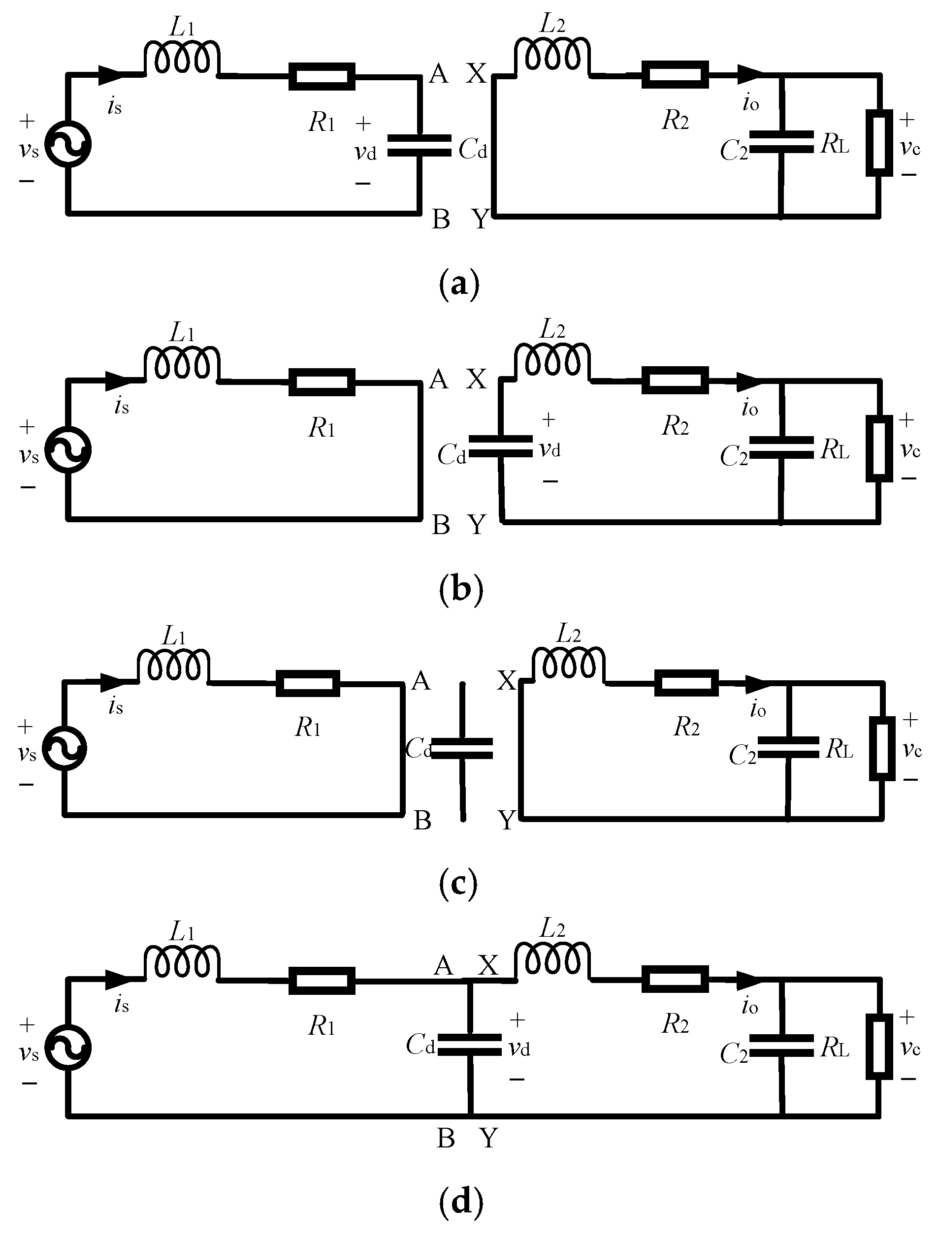
2. The Topology and Modulation Principle of Six-Switch Converter
The topology of the six-switch converter is shown in
Figure 1. Each bridge arm is composed of three switches in series, and there are two sets of input and output. Compared with the traditional single-phase back-to-back AC-DC-AC converter, the proposed converter reduces two switches. In the proposed six-switch converter, the switch in the middle of each bridge arm is shared by the rectifier and inverter, and the voltage
vXN is no greater than
vAN at any time. As shown in
Table 1, each bridge arm of the six-switch converter has three switching states.
In order to meet the switching constraint requirements of the six-switch converter, the modified carrier-based PWM method is applied, and the modulation reference of the upper rectifier and the modulation reference of the lower inverter are compared with a common triangular carrier, respectively, as shown in
Figure 2.
The instantaneous value of the upper reference must be no less than the lower reference. The PWM signal of switch
ST1 (
ST3) is generated by comparing the upper (lower) reference and the triangular carrier, and the PWM signal of switch
ST2 is generated by logic operation.
where
vcw is the common triangular carrier,
vrA and
vrX are the upper and the lower modulation references, respectively.
Figure 3 shows the modulation references of
ST1,
ST3,
ST4,
ST6 in a six-switch converter. It can be observed that due to the relative position changes of the four references in one line frequency cycle, the switching signals of the six switches also change. Therefore, the relative position in a line frequency cycle can be divided into four states (two for the first half cycle and two for the second half cycle) for analysis. Take the first half line frequency cycle of the modulation reference as an example to analyze the working states of the circuit.
There are four working states of the six-switch converter, which are introduced as follows. The rectification state (abbreviated as RS) is shown in
Figure 4a, the inversion state (abbreviated as IS) is shown in
Figure 4b, the freewheeling state (abbreviated as FS) is shown in
Figure 4c, and the both-way state (abbreviated as BS) is shown in
Figure 4d. When the relative positions of four modulation references are shown as state A in
Figure 3, the six-switch converter has the first three working states in one switching cycle. When the relative positions of four modulation references are shown as state B in
Figure 3, the six-switch converter has all four working states in one switching cycle.
From the aforementioned six-switch converter modulation method, a schematic diagram of six switching states in one switching cycle can be achieved, as shown in
Figure 5. The state A in
Figure 5a corresponds to the state A in
Figure 3, which means the relative positions of the modulation references are consistent. State B in
Figure 5b corresponds to state B in
Figure 3.
vcw,
vrA, and
vrX were previously defined on paper, and
vrB and
vrY are the modulation references of the upper switch and the modulation references of the lower switch of the second bridge arm, respectively.
d1,
d3,
d4, and
d6 denote the duty ratios of
ST1,
ST3,
ST4,
ST6, and
TS is the switching period. From
Figure 5a, it can be concluded that when the switching states of
ST1~
ST6 are {101011}, the six-switch converter is in RS, and the state duration is (
d1–
d4)
TS. When the switching states of
ST1~
ST6 are {110101}, the six-switch converter is in IS, and the state duration is (
d6–
d3)
TS. The rest of the switching states are in FS, and the state duration is (1 −
d1 + d3 + d4 −
d6)
TS. 3. Improved Modulation Strategy Analysis of Six-Switch Converter Based on Time Average Modulation
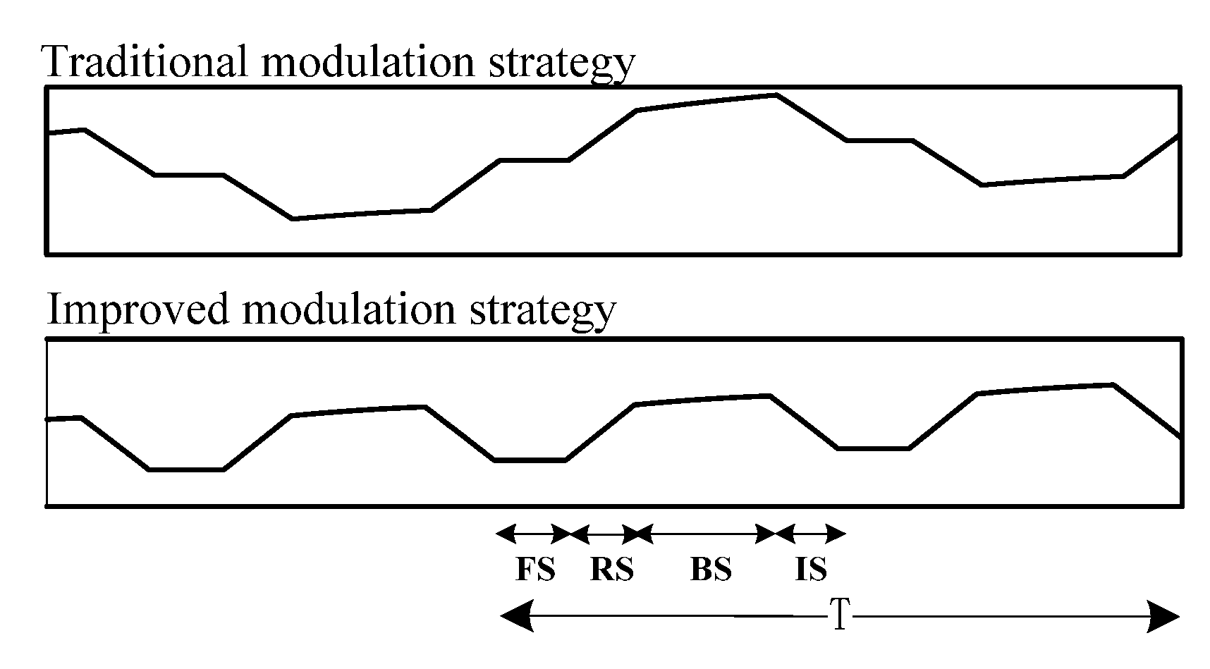
It is assumed the inversion and rectification have the same power factor. Under the traditional six-switch converter control strategy, one switching cycle includes eight working states, followed by FS, RS, FS (BS in state B), IS, FS, IS, FS (BS in state B), RS. Two RS (or IS) are too close, and there is only one FS between them, so that the DC side capacitor is continuously charged (or discharged). A large capacitor is required, which greatly limits practical applications of the six-switch converter. The key point of the proposed improved modulation method is to exchange rectification state and inversion state in the second half of the switching cycle by logic control, so that the order of the eight states in a cycle becomes FS, RS, FS (BS in state B), IS, FS, RS, FS (BS in state B), IS. Therefore, the energy on the capacitor can quickly accumulate and release in a complete switching cycle, achieving the effect of ‘fast charging and discharging’.
Figure 6 shows a larger version of the DC side capacitor voltage
vd under two modulation strategies. Each linear section in the curve corresponds to FS, RS, IS, and BS, respectively.
According to the input/output power balance theory and supposing
VS ≈
VAB ≈
VXY, the Equation (2) can be obtained by vector relations. Where
X1 is the input impedance and
X2 is the output impedance.
θ1 represents the phase angle of rectification modulation reference and
θ0 is the power factor angle of inverter load. When the radio of
X1/
X2 is about 0.2, the unit input power factor can be ensured.
The voltage fluctuation of the DC side capacitor is caused by the fluctuating current flowing through the capacitor, as shown in Equation (3). When the amplitude of
ic becomes smaller, the capacitor which used to keep
vd relatively stable also decreases. In order to verify the effectiveness of the improved six-switch converter modulation strategy, the
ic under the traditional and improved modulation strategies are calculated and compared respectively.
The equation of Kirchhoff’s Current Law at point P of six-switch converter in
Figure 1 is:
In (4),
i1(
t) and
i4(
t) are currents flowing through switch
ST1 and
ST4 based on the pre-defined reference direction. The average value of current
i1(
t) can be calculated according to the switching state of the six-switch converter. When the switching states of
ST1,
ST2,
ST3 are {011},
i1(
t) = 0; when the switching states becomes {101},
i1(
t) =
is(
t) with the duration of (
d1 + d3 − 1)
TS; when the switching states are {110},
i1(
t) =
is(
t) −
io(
t) with the duration of (1 −
d3)
TS. Therefore, the average current
i1(
t) can be written as:
Similarly, when the switching states of
ST4,
ST5,
ST6 are {011},
i4(
t) = 0; when the switching states are {101},
i4(
t) =
is(
t) with the duration of (
d4 + d6 − 1)
TS; when the switching states are {110},
i4(
t) =
is(
t) −
io(
t) with the duration of (1 −
d6)
TS. So, the average current
i4(
t) can be written as:
Substitute (5) and (6) into (4), average current
ic can be figured out as:
Modulation reference for rectifier is defined as:
Modulation reference for inverter is defined as:
where
mr and
mi are modulation indices for the rectifier and inverter, respectively. Assuming unity input power factor operation condition,
φ is phase angle difference between rectifier reference and inverter reference.
Duty radios
d1,
d3,
d4,
d6 can be calculated through similar triangle theory:
Parameters doff1 and doff2 are offset values utilized for moving up/down modulation reference of rectifier/inverter.
Finally, substitute
d1,
d3,
d4 and
d6 into Equation (7):
where
is(
t) is expressed as
Is sin
wt, the phase angle of inversion modulation reference is (
wt + θ1 + φ), so the output voltage
vxy is also (
wt + θ1 + φ). Since the output current
io lags behind the inversion output voltage
vxy, the output current’s phase angle is (
wt + θ1 + φ − θo).
θo is the power factor angle of inverter load, thus
io(
t) can be expressed as
Iosin(
wt + θ1 + φ −
θo). The angle relationship of proposed converter is shown below.
The constant term in Equation (15) is identical to zero based on the assumptions of no switching or capacitor loss.
Amplitude of current
ic can be gotten as below through expansion of (16).
It is observed from (17) that when phase angle
φ reaches (
θo −
θ1)/2, minimization of AC power variation can be achieved in DC-link voltage. Therefore,
φ is equal to (
θo − θ1)/2 in this paper and modulation indices for rectifier and inverter are supposed to be approximately the same (
mr =
mi =
m).
Icmin under traditional control can be written as:
Ic′ under improved control can be attained in the same way. When the switching states of
ST1,
ST2,
ST3 are {011},
i1′(
t) = 0; when the switching states are {101},
i1′(
t) =
is(
t) with the duration of ((
d1 + d3 + d4 + d6)/2 − 1)
Ts; when the switching states are {110},
i1′(
t) =
is(
t) −
io(
t) with the duration of ((
d1 −
d3 −
d4 −
d6)/2
+ 1)
Ts. Therefore, the average current
i1′(
t) can be written as:
Similarly, when the switching states of
ST4,
ST5,
ST6 are {011},
i4′(
t) = 0; when the switching states are {101},
i4′(
t) =
is(
t) with the duration of ((
d1 + d3 + d4 + d6)/2 − 1)
Ts; when the switching states are {110},
i4′(
t) =
is(
t) −
io(
t) with the duration of (1 −
d6)
Ts. So, the average current
i4′(
t) can be written as:
Substituting
d1,
d3,
d4 and
d6 into Equation (20), it yields:
The constant term in Equation (22) is identical to zero based on the assumptions that no switching or capacitor loss.
Amplitude of current
ic can be got as below through expansion of (23).
Ic’ can reach its minimum when
φ =
θo −
θ1:
The above has been obtained
Icmin = 0.5
m|
Io −
Is|. Subtracting Equation (18) from (25) to compare the amplitude, it yields:
It can be known Icmin > Ic′min from (26). The calculation result shows that improved modulation strategy reduces the amplitude of Ic and the DC side voltage fluctuation. Therefore, a smaller capacitor Cd can be used to maintain the relative stability of the DC voltage vd, thereby achieving the purpose of reducing the capacitance.
The derivations of Icmin and Ic′min have already reflected the difference of modulation strategy. Therefore, whether the improved modulation strategy is effective can be judged by observing the fluctuation of DC side capacitor voltage under the line frequency cycle.
4. Simulation and Experimental Results
In order to further verify the feasibility and correctness of the proposed modulation strategy, a linear-load typical system with unity input power factor is built on the Matlab/Simulink platform. The simulation results based on traditional and improved modulation strategy, respectively, are compared to prove the validity of the improved strategy. Simulation parameters are shown in
Table 2.
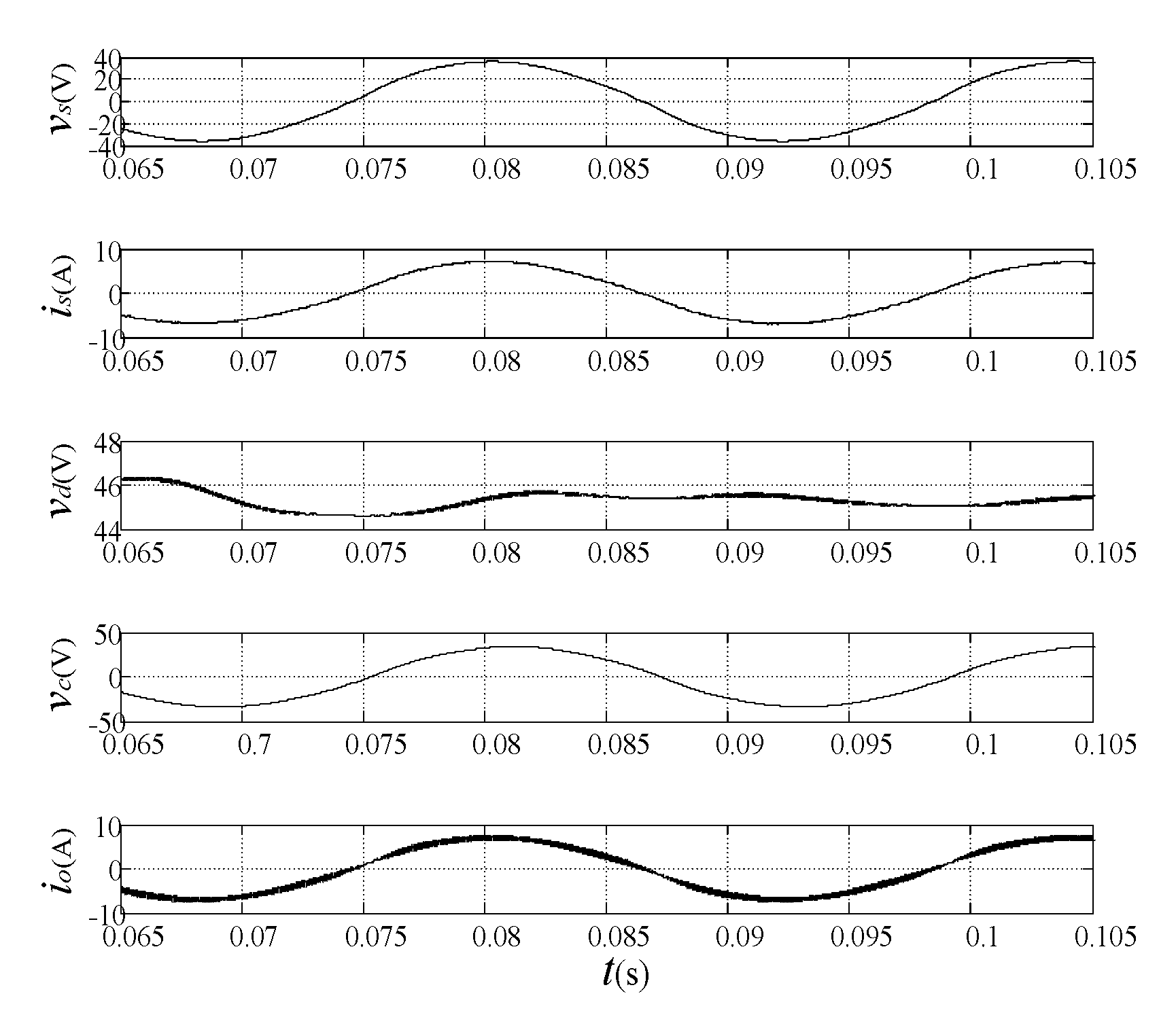
Figure 7 shows the waveforms of input/output voltage, current, and DC-link voltage under traditional control when
φ is equal to 0.4. The percentage of DC-link voltage variation is limited into 2.71% (1.24 V/45.81 V = 2.71%), and total harmonic distortion (THD) of the output voltage
vc is 1.39%.
Figure 8 shows the waveforms of input/output voltage, current, and DC-link voltage under improved control when
φ′ is equal to 0.8. The percentage of DC-link voltage variation is limited to 0.56% (0.225 V/45.28 V = 0.56%), and total harmonic distortion (THD) of the output voltage
vc is 0.22%.
Seen from the simulation results, the proposed modulation strategy can reduce DC-link voltage variation under the line frequency. Therefore, DC-link voltage vd can remain relatively stable with a smaller capacitor. At the same time, the THD of improved output voltage drops significantly and the waveform is better.
Through (17) and (24) in the previous section,
Ic =
Ic′ can be attained when phase angle difference is equal to zero. At this point, it should be observed that the DC-link voltage fluctuations are equal under the line frequency cycle, regardless of which modulation strategy is adopted, as shown in
Figure 9.
Seen from the above figure, the voltage fluctuations of the DC side under the line frequency cycle are equal. Comparing the ripples under the switching cycle, clearly, the ripple under the traditional modulation strategy is larger than the ripple under the improved modulation strategy (the yellow envelope is thicker than the green one in the figure above), which demonstrates again the effectiveness of improved modulation strategy under switching period scale.
When only the DC-link capacitance
Cd is changed, the DC-link ripple coefficient, amplitude and THD of output voltage under traditional modulation strategy and improved modulation strategy are shown in
Table 3 and
Table 4.
Figure 10 intuitively depicts the trends of ripple coefficient changing with
Cd under two modulation strategies, respectively. As
Cd increases, the DC-link voltage fluctuation should reduce. However, when the capacitor is small, DC-link voltage waveform under the line frequency cycle is mainly caused by the oscillation under the switching cycle. In fact, the magnitude of voltage fluctuation under the switching cycle still shows a decline trend.
In order to further prove the theoretical analysis of the proposed converter, an experimental prototype is made in laboratory. Specifications of the prototype are the same as
Table 2. The prototype block diagram, experimental setup, and the top-view of the proposed converter are shown in
Figure 11a–c, respectively. Notice that the converter is operated in an open loop and the driving signal is generated by RCP and FPGA EP4CE10F17C8.
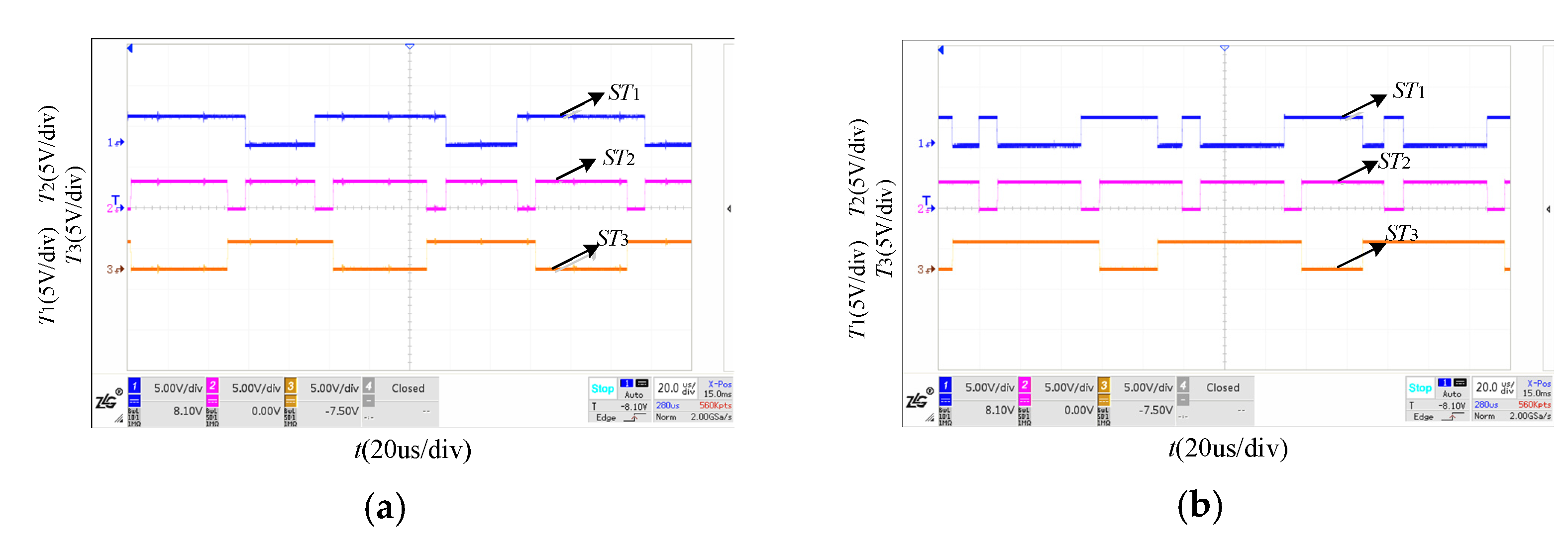
The switching control signals of the upper, middle, and lower switches on the same bridge arm generated by RCP and FPGA are shown in
Figure 12.
Figure 12 shows that the switch sequence is consistent with the theoretical analysis and simulation results. The final output waveforms are shown in
Figure 13.
Seen from
Figure 13, the percentage of DC-link voltage variation is 3.49% (1.6 V/45.9 V = 3.49%) under the traditional modulation strategy while the percentage of DC-link voltage variation is 2.20% (1 V/45.4 V = 2.20%) with the improved modulation strategy.
Compared with the experimental results, the improved modulation strategy can reduce the DC-link voltage fluctuation greatly under the line frequency, which once again verifies the effectiveness of the proposed modulation strategy.
Fourier analysis of
vc under the traditional modulation strategy and the improved modulation strategy are shown in
Figure 14a,b, respectively.
The THD of the output voltage under the traditional modulation strategy is 1.38%, and correspondingly, the value under the improved modulation strategy is 0.92%, which proves that the proposed modulation strategy can reduce the DC side voltage ripple coefficient under the line frequency, thereby improving the output voltage waveform.
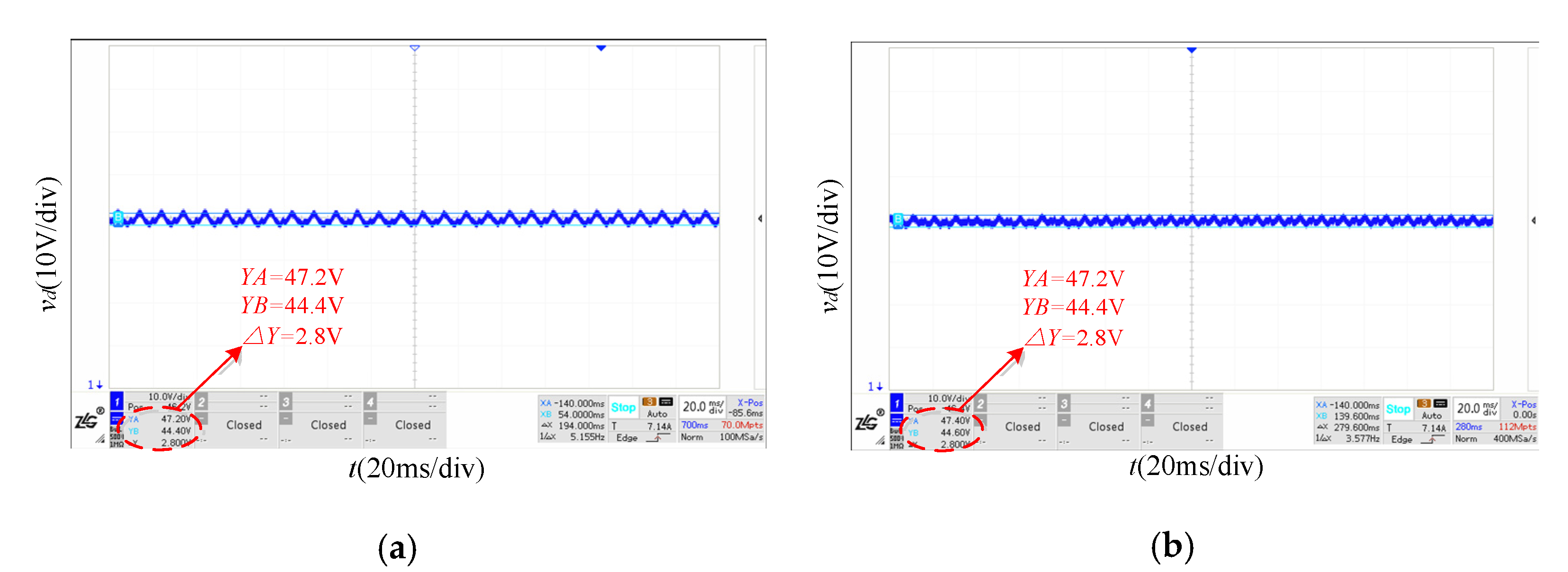
When the phase angle
φ equals to zero, according to theoretical derivation, the ripple coefficients under the traditional and improved modulation strategies should be equal. The experimental results are shown in
Figure 15.
In
Figure 15a,b, the position and spacing of cursors A and B are equal. It can be observed that the voltage fluctuations under the traditional and improved modulation strategies are almost the same (the delay of the controller itself cannot be ignored).
The stable operation of the system can be strictly ensured when the ripple coefficient is less than 2%. When the ripple factors under traditional strategy and improved strategy are both about 2%, the required DC-link capacitors are shown in
Figure 16.
It can be observed from
Figure 16 that when the voltage ripple is about 2%, the six-switch converter adopting the traditional modulation strategy requires capacitance value of 1800 μF, while the improved one requires capacitance value of 500 μF. The capacitance value is greatly reduced, and long-life film capacitors can be used to replace the large electrolytic capacitors to realize the electrolytic capacitor-less solution of the six-switch converter.


