Abstract
The current understanding of physical principles governing electronic transport in graphene field effect transistors (GFETs) has reached a level where we can model quite accurately device operation and predict intrinsic frequency limits of performance. In this work, we use this knowledge to analyze DC and RF transport properties of bottom-gated graphene on boron nitride field effect transistors exhibiting pronounced velocity saturation by substrate hyperbolic phonon polariton scattering, including Dirac pinch-off effect. We predict and demonstrate a maximum oscillation frequency exceeding . We discuss the intrinsic limit of GFETs and envision plasma resonance transistors as an alternative for sub-THz narrow-band detection.
1. Introduction
Graphene is considered as a high-potential material for electronics, especially radio-frequency (RF) field effect transistors (GFETs) [1], owing to the high intrinsic mobility of charge carriers [2,3,4,5]. The main challenge in this respect is to achieve current saturation at high bias to obtain significant voltage and power gain. Two routes are considered. The first relies on band-gap engineering using, e.g., lateral confinement in graphene nanoribbon devices [6], which is often obtained at the cost of a reduced mobility. As in MOSFETs [7], the saturation results from a potential barrier induced at the drain side. The second route is velocity saturation, which promises high performances [8,9,10]. It requires high mobility transistors () and results in large saturation currents () [11]. Limited by the Fermi energy at low doping, the saturation velocity is determined by optical phonon (OPs) scattering at large doping when exceeds the optical phonon energy [11,12]. In oxide-supported graphene, relevant OPs are substrate polar phonons (SPPs) [13,14,15] that have a moderate energy . The saturation current being proportional to the OP energy, power applications favor non-oxide dielectrics such as SiC (), or hexagonal boron nitride (h-BN), which has two Reststrahlen bands, and , associated respectively with out-of-plane and in-plane optical phonons. Uniaxial dielectrics, such as h-BN, actually sustain hyperbolic phonon polariton modes (HPhPs) that differ from SPPs (and intrinsic OPs), insofar as they propagate deep in the dielectric bulk, providing a unique radiative cooling pathway [11,16]. This paper discusses velocity saturation GFETs, their optimal design and operating conditions, their intrinsic frequency limit, and envisions the possibility to overcome this limit using plasma resonance devices [17,18]. It relies on experimental data taken on two series of h-BN-supported GFETs based on CVD graphene, which is appropriate for wafer scale applications.
2. Methods
Samples used in this work are made of CVD graphene on a thin h-BN flake deposited on top of a metallic bottom gate. The substrate consists in a thermal insulating barrier on top of high-resistivity Si suitable for RF measurements. Two types of gate electrodes are used: a thin tungsten electrode deposited on (type A samples) for low-frequency devices and DC characterization, and a thick gold dual gate buried in (type B samples) for RF devices. Several samples of both types have been measured presenting similar characteristics, but for simplicity, we focus on one illustrative sample of each type.
Sample-A (Figure 1a) is made out of a 20-nm-thin tungsten film that is etched to define the gate whose dimensions are μm for the length and μm for the width. In addition, we have included local contact gates (also tungsten) controlling the carrier density of the contacted graphene to reduce the contact resistance (see [19]). An h-BN flake, of thickness , is deposited on top of the gate by a dry transfer technique [2]. The h-BN surface is cleaned by furnace annealing at 300 °C under an Ar/H2 flow. The CVD graphene is grown on copper following the pulsed CVD method at Institut Néel [3] and transferred with a wet technique on top of h-BN. Again, the polymer residues are removed by furnace annealing. Finally, of Pd is evaporated for the electrical contacts, and devices are embedded in a 50 -matched coplanar waveguide (CPW) used for DC and RF characterization. A schematic of a type-A device can be seen in Figure 1b. In very-high mobility devices such as the Zener-Klein transistor of [11] radiative cooling by hyperbolic phonon polaritons in the can be achieved, which is optimized using thicker () h-BN substrates. Note also that alternative WSe2 substrates can be used that provide even higher mobility at room temperature [20].
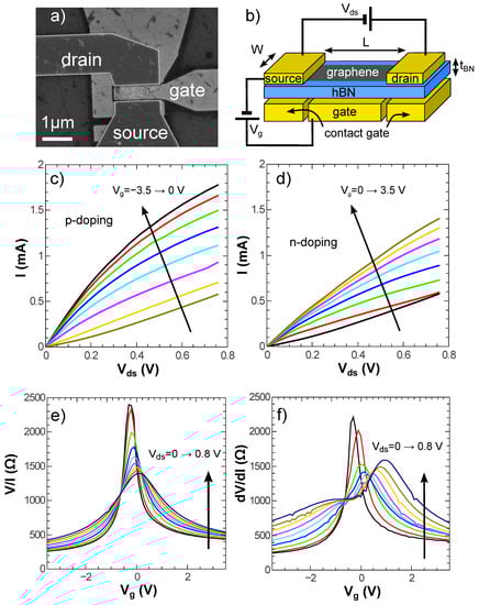
Figure 1.
Low frequency field effect transistors (GFETs). (a) SEM image of sample-A. Note the absence of ungated area. (b) Electrical sketch of samples used in this study. For sample-A we have , μm and . (c) I–V characteristic of sample A in the p-doping regime. (d) I–V characteristic of sample-A in the n-doping regime. (e) DC resistance of sample-A. (f) RF small signal resistance of sample-A. The global increase of resistance with is due to HPhP scattering only for negative gate voltages and both HPhP scattering and Dirac pinch-off for positive gate voltages. The resistance peak of is the best working point for an RF transistor.
The fabrication steps of sample-B (see Figure 2a below) are identical, except for the gate electrode: First a trench of is realized with e-beam lithography and dry etching with a carefully controlled depth of . Another e-beam lithography step defines a gate electrode within the trench, and gold is evaporated up to a nearly perfect alignment with the surface (an excess of a few of gold is preferable to avoid any air gap between the gate and h-BN). The gate dimensions are μm and μm, and h-BN thickness is .
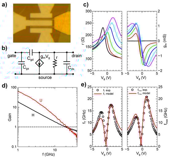
Figure 2.
Radio-frequency GFETs. (a) Optical image of sample-B before graphene and contact deposition. Dimensions: , μm and . (b) Small signal lumped elements circuit of an RF transistor. (c) RF small signal resistance r and transconductance of sample-B measured at for biases in the 0–2 range. (d) Logarithmic plot of the current H(f) and Mason U(f) gains measured between 1 GHz and 40 GHz after de-embedding. (e) dependence of the corresponding measured cut-off frequencies (black circles) together with the model prediction (red lines).
The low contact resistance of sample-A (μm) is minimized by contact gating implying that the total resistance is dominated by the channel. Fully ambipolar contact gating was demonstrated in Ref. [19]; in this work the channel length was small so that the transistor was controlled by the contact junction resistance. Here we work with long channels, longer than the optical phonon scattering length, to realize velocity saturation transistors with large voltage gain; contact gating is used instead to minimize the contact resistance. This geometry is well suited for the identification of such mechanisms and their modeling. The sample-B geometry is best suited for maximizing the oscillation frequency , as dual gates provide a better impedance match of the device and the thick gold allows a reduction of the gate electrode resistance, which is a limiting factor for . Our devices fulfill the filed-effect mobility requirement at low temperature. Experiments are carried out in a Janis cryogenic probe station at in the band 0–. A vector network analyzer (VNA) is used to measure the S-parameters of our transistors.
3. Characterization of Low-Frequency GFETs
Figure 1c,d shows the I–V characteristic of sample-A in the p-doping and n-doping regime respectively. Both regimes show a trend toward saturation, with larger currents on the p-side due to a lower contact resistance (the contacted graphene is p-doped at ~ by the contact gate kept at a constant voltage here). Figure 1e shows sample-A’s DC resistance for increasing bias voltages . In the low doping regime, there is a broadening of the resistance peak as is increased, which we attribute to a thermal effect. More interestingly, in the highly doped regime, we observe an increase of the resistance which is generally attributed to optical phonon scattering. However the relevant quantity is rather the small signal resistance , shown in Figure 1f, which is directly obtained from the S-parameters and averaged over a to bandwidth. Indeed, on one hand, the small signal resistance is more sensitive to current saturation and on the other hand, it is used to describe the operation of an RF transistor [21]. In addition to the increase of resistance in the doped regime, we observe a pronounced shift of the resistance peak towards positive gate voltages (the resistance peak shifts towards negative when is negative). This peculiar shape is characteristic of locally gated devices [11] and not observed when using a remote Si gate. This effect, already introduced in Refs. [8,22], is a consequence of finite quantum capacitance effects and geometry which lead to a non-uniform carrier density in the channel at large and eventually to a Dirac pinch-off. The next section is devoted to the development of a comprehensive model taking into account both mechanisms.
4. Simple Model of GFETs
4.1. Substrate Phonon Scattering Model
The scattering by optical phonons has been identified as an important phenomenon of high-bias transport in high mobility materials like carbon nanotubes [23]. However, the influence of the substrate cannot be neglected, and the impact of surface polar phonons (SPP) on transport properties has been invoked in several studies to explain the current saturation [8,12,14,15,24]. Those studies have been conducted with graphene on oxide samples, and to our knowledge, the effect of HPhPs has only recently been demonstrated using high-mobility exfoliated graphene on h-BN transistors [11]. It was found that velocity saturation is provided by the lower -HPhP band and hot electron cooling by the upper -HPhP band. The out-of-plane optical phonons of the band lift the sublattice degeneracy of graphene leading to an (unscreened) electron–phonon coupling reminiscent of the mass disorder mechanism reported in Ref. [25]. In Refs. [11,16] exfoliated graphene was used and the mobility was high enough () to access interband transport at very high bias, the so-called Zener–Klein regime, which is not reached in the present study due to limited mobility.
The heuristic model used to describe HPhP scattering is inspired by the optical phonon-electron scattering model used by Yao et al. for carbon nanotubes [23]. One considers that electrons are accelerated by an electric field up to the HPhP energy (here ) to emit a phonon. In this notation, is the voltage across the channel without potential drop at the contacts. This interaction can be expressed as a scattering length for the electron–HPhP interaction , which is density-independent as represented by the dashed lines in Figure 3a for different electric fields. Our samples are not totally ballistic, and we need to account for a finite impurity scattering length , shown as a black solid line (the effective mobility is ). The resulting scattering length is given by the Matthiessen rule , which is shown at V in Figure 3a as a green solid line. As seen in the figure, at high bias, the transport is indeed dominated by HPhP scattering. The total scattering length is translated into conductance . It can be more conveniently expressed as a resistance:
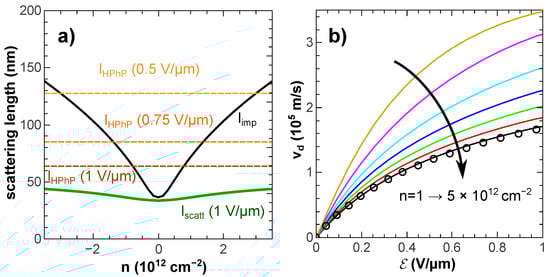
Figure 3.
(a) Scattering length associated with the impurity scattering (black solid line) responsible for the low field mobility; here , and with the HPhP scattering (dashed lines) for different in plane electric fields . The green thick line is the total scattering length at the largest bias obtained by the Matthiessen’s law. (b) Carrier drift velocity simulated using with R from Equation (1), and the measured drift velocity at large doping () in black circles.
The first term of Equation (1) is the ballistic resistance, the second is the well-known diffusive term, and the third corresponds to the HPhP scattering contribution; it is responsible for saturation and proportional to . Note that the linear dependence of the DC resistance (negative quadratic deviation in the current) depends only on the carrier density and the HPhP energy. That is how we can identify the energy of h-BN HPhPs as the main source of scattering and rule out the scattering by intrinsic graphene optical phonons or the -HPhP band, as ~~. Note that the role of intrinsic OPs or -HPhPs in energy relaxation can be identified using noise thermometry respectively in suspended [26] and h-BN supported graphene [11,16]. This illustrates the difference between momentum relaxation (the resistance) and energy relaxation (the temperature or electronic distribution) mechanisms (Another example of such a difference, is acoustic phonon scattering which gives rise to a linear temperature dependence for resistivity but a cubic one for relaxation, reflecting single phonon and inelastic supercollision scattering respectively [27]).
In the full saturation regime all terms are negligible compared to the HPhP term and one obtains the saturation current:
Physically, the current saturation is due to the carrier velocity saturation :
Equations (1)–(3) strictly hold at large doping when ; the crossover to Fermi energy limited current at low doping can be taken into account by substituting for [11] (The pre-factor, which stems from the angular projection of electron momentum along the current axis, is sometimes omitted in the literature [8]). In Ref. [11] the saturation current was deduced by fitting the differential conductance by the law , which can be deduced from Equation (1). The saturation is not complete in our samples due to limited mobility and we cannot extract and directly. In Figure 3b, we show the calculated drift velocity as a function of (solid lines) for different densities from the current saturation model with . Further, we show the measured at large density (), where channel density is mostly homogeneous. The very good agreement between theory and experiment, in a regime where HPhP scattering dominates, confirms the relevance of our model.
As a conclusion of this section, we note that the effect of high mobility is mainly to decrease the threshold voltage of saturation and thus to clarify the transition toward the current saturation regime. This is why full current saturation is only observed in high-mobility samples.
4.2. Dirac Pinch-Off Model
In a remote gate transistor, for example using a global silicon gate, the gate uniformly controls the charge of the semiconducting channel. However, considering a local gate transistor, where local means that the quantum capacitance and the geometrical capacitance per unit area are on the same order of magnitude, the charge in the channel is not set by the gate voltage only and it can be influenced by the electrostatic potential in the channel. Applying a voltage on the drain electrode results in a linear electrochemical potential along the channel if we assume diffusive conduction, which is the case at large bias due to HPhP scattering. We write the electrochemical balance at the position x in the channel:
where is the electrostatic potential of graphene. This equation is combined with the electrostatic equilibrium , which allows calculating :
with and . It results in an inhomogeneous within the channel. This effect is sketched in Figure 4a, and the calculated is shown in Figure 4b for increasing . The corresponding carrier density in the channel as a function of and x is shown in the color plot of Figure 4c. Starting from an n-doped channel and increasing leads to a decrease of the carrier density on the drain side. Figure 4b shows that the neutrality can be reached and that for larger there is even a localized neutral point whose location is shifted toward the source electrode. At the onset of neutrality on the drain side, increasing induces an increase of the resistance, which amplifies the sublinear behavior of the I–V characteristic and results in enhanced current saturation. This is the Dirac pinch-off. On the contrary, starting from a p-doped channel, an increase of leads to an increase of the carrier density on the drain side which contributes to decreasing the channel resistance. This explains the observed asymmetric shape of the high bias resistance curve in Figure 1f.
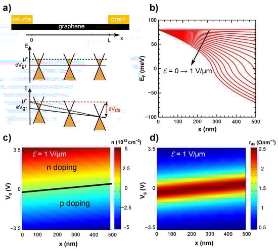
Figure 4.
(a) Sketch of the doping profile across the graphene channel when is increased. Starting from n-doping, can be decreased down to neutrality at the drain side. This is the Dirac pinch-off. (b) Simulated along the channel for increasing in-plane electric field. (c) Color plot of the local carrier density in the channel as a function of the x-position along the channel and the gate voltage (d) Color plot of the local resistivity at V. The total resistance of the device is the integration over x of this resistivity.
4.3. Hot Electron Effects
To accurately describe the behavior of our transistor, we have to take into account the thermal broadening that arises at large . Indeed, for high biased samples, the electronic temperature can rise up to 800 K [28], which significantly modifies the energy distribution. We take into account this thermal broadening by writing the carrier density with a residual term that depends on :
where is the sum of an impurity term ( at zero bias) and a hot electron term: ~. Here, is governed by the interaction between electrons and acoustic phonons of graphene. It has been shown in previous studies [27] that, at low doping and moderate impurity scattering, electron cooling is controlled by electron–phonon-impurity supercollisions and that for a given Joule power input one has (In very high mobility h-BN supported/encapsulated samples, supercollisions are suppressed and the leading relaxation mechanism becomes black-body and luminescent -HPhP emission). In this equation we have and so that is constant. Finally, the hot electron residual density reads as follows,
where is a constant that depends on sample dimensions. This is used to calculate the local resistance , which is plotted in Figure 4d. for V. As expected, the maximum resistance line follows the minimum carrier density line, with a width related to .
4.4. Complete Model and Discussion
Let us now calculate the total resistance of the graphene channel taking into account HPhP scattering, the non-uniform carrier density in the channel and the hot electron effect. We compute the total scattering length and neglect the ballistic conductance to obtain the local resistance
The total channel resistance is then obtained by integrating over the channel length:
Finally, in short devices with high-mobility graphene, the contact resistance is not negligible. Most of the contact resistance comes from the junction between contacted graphene and the channel. This issue has been overcome in a previous study with the transistor geometry of sample-A [19]. It allows us to calculate the dependent contact resistance. The total transistor resistance is then . For sample-A, we have on the p-doping side (where there are p-p junctions at the two contact edges) and on the n-doping side (where there are p-n junctions at the two contact edges).
The relevant quantity for an RF transistor is the small signal resistance that we calculate from the current through the transistor and the applied bias voltage across the device. The simulated is plotted in Figure 5a where the mobility and are determined from the zero bias transfer curve and the thermal broadening coefficient (from [28]) is in principle universal. The very good agreement between measurement and simulation shows that we are able to accurately predict the behavior of a local gate transistor driven at high bias knowing the graphene mobility, the contact resistance and the substrate phonon energy. It validates our transistor model and confirms the role of the h-BN HPhPs at in velocity saturation. To emphasize the effect of the local gate on the saturation we plot in Figure 5b, a simulation for a substrate thickness of where all parameters are conserved (apart from which is adjusted to conserve the zero bias density). There is a significant difference between local and remote gate on the shape of the transfer curve. In Figure 5b, the slight asymmetry between p and n doping comes from the contact resistance difference.
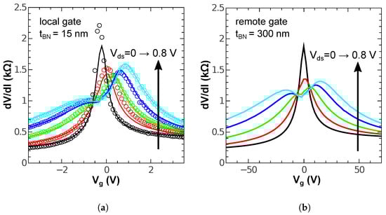
Figure 5.
(a) Small signal resistance of the transistor obtained from the model (solid lines) and from the measured scattering parameters of sample-A at (circles). (b) Small signal resistance simulated for a remote gate transistor (h-BN dielectric thickness of ). The saturation effect is enhanced for the local gate device in the n-doping regime.
5. Characterization of RF-GFETs
The performance of Sample-A as an RF transistor is assessed at high frequency. Measuring the S-parameters gives a direct access to the channel small signal resistance r and the transconductance shown in the schematic of Figure 2b. We also measure the current gain H and the Mason gain U (equivalent to the power gain). Those gains are sensitive to extrinsic parameters such as stray capacitances and, for U only, the resistance of the gate electrode. After removing the effect of stray capacitances by a de-embedding procedure, we obtain the current gain cut-off frequency and the Mason’s gain cut-off frequency . The fact that ~ is a distinctive feature of velocity saturation GFETs, as in mobility-limited GFETs [29]. The value of is limited here by the large resistance ~ of the tungsten gate electrode. This is why we built a thick gold gate device in sample-B (shown in Figure 2a).
In sample-B, the channel width is also further increased to μm, to increase the total current in the device. In terms of , however, a compromise has to be found between a large current which means a large transconductance and a larger gate resistance which strongly limits . The small signal characteristics of sample-B, i.e., the resistance r and transconductance , are plotted in Figure 2c. One can notice the strong saturation effect on the n-side where the high bias r is larger than the zero bias resistance peak. In this sample, the n-side is also the low contact resistance side which results in a larger on the n-side. Both effects contribute to a larger voltage gain for positive gate voltages. This is confirmed by measuring H and U at the maximum bias and plotted in Figure 2d after de-embedding. In Figure 2e, we plot the -dependence of and at V. Our model allows estimating r and which is useful to determine the transistor’s figures of merit from and
The predicted and in Figure 2e compare fairly well with our measurement. Both figures of merit present two peaks for p- and n-doping. In the case of , the peak asymmetry comes from the contact resistance asymmetry. For the peak asymmetry is stronger because it is also sensitive to a stronger saturation on the n-doping side.
The availability of a reliable model allows fine tuning parameters to optimize . It appears that in our sample the large gate resistance is the main limitation. Engineering the transistor extrinsic elements can improve by a large factor, for example, by using a T-shaped gate [9,30]. Another important limiting factor is the contact resistance.
6. Perspectives on High-Frequency Graphene Devices
In an attempt to assess the intrinsic frequency limits of GFETs, we include here an analysis of Zener–Klein transistors where contact resistance is low enough, mobility is large enough and channel length long enough ( μm), to access a fully developed inter-band Zener–Klein tunneling regime [11]. A quasi perfect current saturation () is achieved thanks to the combined intraband velocity saturation, interband Zener–Klein tunneling and Dirac pinch-off (Figure 1 of Ref. [11]). The small contact resistance , large DC transconductance , and saturation resistance lead to a large voltage gain . From these numbers, we estimate (taking in Equation (10)) translating to (taking with μm and ). Considering the optimization of saturation velocity, contact resistance and channel length, these figures constitute the intrinsic frequency limit of GFETs. It still remains to be demonstrated with edge-contacted, h-BN encapsulated, GFETs at room temperature.
This intrinsic limitation of GFETs can be circumvented relying on collective modes such as plasmons which benefit from an enhanced velocity appropriate for sub-THz operation. This corresponds to plasma resonance transistors (PRTs) [18], which are multi-mode narrow-band detectors. Intrinsic Dirac-fermion plasma modes can be studied in plasma resonance capacitors (PRCs), which behave as quarter-mode resonators (fundamental at and harmonics ). In a recent study [17], an h-BN encapsulated PRC working at () was demonstrated, showing the relevance of long-wavelength plasma resonance devices in fully characterizing high-mobility graphene, offering a full analysis of the temperature and density dependence of the quantum capacitance , kinetic inductance and damping or mean-free path .
7. Conclusions
We have fabricated, modeled, and measured high-performance velocity-saturation GFETs showing promising perspectives for microwave detection and amplification. Our modeling involves physical insight into microscopic mechanisms of velocity saturation and a proper account of Dirac pinch-off effects. Our work allows assessing the intrinsic frequency limits of GFETs using velocity saturation associated with Zener–Klein tunneling and opens perspectives “beyond-GFETs”, using plasma resonance techniques for sub-THz detection. The figure of merit is the ratio which increases from in the mobility-limited regime, over ~1 in the velocity-saturation regime, up to in the Zener–Klein regime. The latter offers promising perspectives in RADAR and GSM applications.
Author Contributions
Q.W., M.B., E.P. and B.P. conceived the experiment. T.T. and K.W. provided the hBN crystals. V.B. provided the CVD graphene. Q.W., M.B., H.G., J.P. and M.R. did the nanofabrication. Q.W., M.B., H.G. and B.P. did the electrical measurements. Q.W., M.B., H.G., D.M., E.B. (Emmanuel Baudin), J.-M.B., G.F., E.B. (Erwann Bocquillon) and B.P. participated to the data analysis and theoretical modelling. Q.W. and B.P. wrote the manuscript with contributions from all coauthors. All authors have read and agreed to the published version of the manuscript.
Funding
The research leading to these results have received partial funding from the European Union Horizon 2020 research and innovation programme under grant No. 785219 “Graphene Core 2”, and from the ANR-14-CE08-018-05 “GoBN”. The work of Q.W. was supported by a DGA-MRIS scholarship.
Acknowledgments
We thank thank L. Becerra for providing the tungsten films.
Conflicts of Interest
The authors declare no conflicts of interest.
References
- Wu, Y.; Jenkins, K.A.; Valdes-Garcia, A.; Farmer, D.B.; Zhu, Y.; Bol, A.A.; Dimitrakopoulos, C.; Zhu, W.; Xia, F.; Avouris, P.; et al. State-of-the-Art Graphene High-Frequency Electronics. Nano Lett. 2012, 12, 3062–3067. [Google Scholar] [CrossRef]
- Wang, L.; Meric, I.; Huang, P.Y.; Gao, Q.; Gao, Y.; Tran, H.; Taniguchi, T.; Watanabe, K.; Campos, L.M.; Muller, D.A.; et al. One-Dimensional Electrical Contact to a Two-Dimensional Material. Science 2013, 342. [Google Scholar] [CrossRef] [PubMed]
- Han, Z.; Kimouche, A.; Kalita, D.; Allain, A.; Arjmandi-Tash, H.; Reserbat-Plantey, A.; Marty, L.; Pairis, S.; Reita, V.; Bendiab, N.; et al. Homogeneous Optical and Electronic Properties of Graphene Due to the Suppression of Multilayer Patches During CVD on Copper Foils. Adv. Funct. Mater. 2014, 24, 964–970. [Google Scholar] [CrossRef]
- Banszerus, L.; Schmitz, M.; Engels, S.; Dauber, J.; Oellers, M.; Haupt, F.; Watanabe, K.; Taniguchi, T.; Beschoten, B.; Stampfer, C. Ultrahigh-mobility graphene devices from chemical vapor deposition on reusable copper. Sci. Adv. 2015, 1, 2375–2548. [Google Scholar] [CrossRef] [PubMed]
- Banszerus, L.; Schmitz, M.; Engels, S.; Goldsche, M.; Watanabe, K.; Taniguchi, T.; Beschoten, B.; Stampfer, C. Ballistic Transport Exceeding 28 m in CVD Grown Graphene. Nano Lett. 2016, 16, 1387. [Google Scholar] [CrossRef]
- Meng, N.; Fernandez, J.F.; Vignaud, D.; Dambrine, G.; Happy, H. Fabrication and Characterization of an Epitaxial Graphene Nanoribbon-Based Field-Effect Transistor. IEEE Trans. Electron Dev. 2016, 58, 1594. [Google Scholar] [CrossRef]
- Sze, S.M.; Ng, K. Physics of Semiconductor Devices, 3rd ed.; John Wiley & Sons: Hoboken, NJ, USA, 2007; p. 293. [Google Scholar]
- Meric, I.; Han, M.Y.; Young, A.F.; Ozyilmaz, B.; Kim, P.; Shepard, K.L. Current saturation in zero-bandgap, top-gated graphene field-effect transistors. Nat. Nanotechnol. 2008, 3, 654–659. [Google Scholar] [CrossRef]
- Guo, Z.; Dong, R.; Chakraborty, P.S.; Lourenco, N.; Palmer, J.; Hu, Y.; Ruan, M.; Hankinson, J.; Kunc, J.; Cressler, J.D.; et al. Record Maximum Oscillation Frequency in C-Face Epitaxial Graphene Transistors. Nano Lett. 2013, 13, 942–947. [Google Scholar] [CrossRef]
- Feng, Z.H.; Yu, C.; Li, J.; Liu, Q.B.; He, Z.Z.; Song, X.B.; Wang, J.J.; Cai, S.J. An ultra clean self-aligned process for high maximum oscillation frequency graphene transistors. Carbon 2014, 75, 249–254. [Google Scholar] [CrossRef]
- Yang, W.; Berthou, S.; Lu, X.; Wilmart, Q.; Denis, A.; Rosticher, M.; Taniguchi, T.; Watanabe, K.; Fève, G.; Berroir, J.M.; et al. A graphene Zener–Klein transistor cooled by a hyperbolic substrate. Nat. Nanotechnol. 2018, 13, 47. [Google Scholar] [CrossRef]
- Barreiro, A.; Lazzeri, M.; Moser, J.; Mauri, F.; Bachtold, A. Transport Properties of Graphene in the High-Current Limit. Phys. Rev. B 2009, 103, 076601. [Google Scholar] [CrossRef] [PubMed]
- Fratini, S.; Guinea, F. Substrate-limited electron dynamics in graphene. Phys. Rev. B 2008, 77, 195415. [Google Scholar] [CrossRef]
- Freitag, M.; Steiner, M.; Martin, Y.; Perebeinos, V.; Chen, Z.; Tsang, J.C.; Avouris, P. Energy Dissipation in Graphene Field-Effect Transistors. Nano Lett. 2009, 9, 1883. [Google Scholar] [CrossRef] [PubMed]
- Perebeinos, V.; Avouris, P. Inelastic scattering and current saturation in graphene. Phys. Rev. B 2010, 81, 5442. [Google Scholar] [CrossRef]
- Baudin, E.; Voisin, C.; Plaçais, B. Hyperbolic Phonon Polariton Electroluminescence as an Electronic Cooling Pathway. Adv. Funct. Mater. 2019. [Google Scholar] [CrossRef]
- Graef, H.; Mele, D.; Rosticher, M.; Stampfer, C.; Taniguchi, T.; Watanabe, K.; Bocquillon, E.; Fève, G.; Berroir, J.M.; Teo, E.T.H.; et al. Ultra-long wavelength Dirac plasmons in graphene capacitors. emph. J. Phys. Mater. 2018, 1, 01LT02. [Google Scholar] [CrossRef]
- Bandurin, D.A.; Svintsov, D.; Gayduchenko, I.; Xu, S.G.; Principi, A.; Moskotin, M.; Tretyakov, I.; Yagodkin, D.; Zhukov, S.; Taniguchi, T.; et al. Resonant terahertz detection using graphene plasmons. Nat. Commun. 2018, 9, 5392. [Google Scholar] [CrossRef]
- Wilmart, Q.; Inhofer, A.; Boukhicha, M.; Yang, W.; Rosticher, M.; Morfin, P.; Garroum, N.; Fève, G.; Berroir, J.-M.; Placais, B. Contact gating at GHz frequency in graphene. Sci. Rep. 2016, 6, 21085. [Google Scholar] [CrossRef]
- Banszerus, L.; Sohier, T.; Epping, A.; Winkler, F.; Libisch, F.; Haupt, F.; Watanabe, K.; Taniguchi, T.; Müller-Caspary, K.; Marzari, N.; et al. Extraordinary high room-temperature carrier mobility in graphene-WSe2 heterostructures. arXiv 2019, arXiv:1909.09523v1. [Google Scholar]
- Schwierz, F. Graphene transistors. Nat. Nanotechnol. 2010, 5, 487. [Google Scholar] [CrossRef]
- Bai, J.; Liao, L.; Zhou, H.; Cheng, R.; Liu, L.; Huang, Y.; Duan, X. Top-Gated Chemical Vapor Deposition Grown Graphene Transistors with Current Saturation. Nano Lett. 2011, 11, 2555–2559. [Google Scholar] [CrossRef] [PubMed][Green Version]
- Yao, Z.; Kane, C.L.; Dekker, C. High-Field Electrical Transport in Single-Wall Carbon Nanotubes. Phys. Rev. Lett. 2000, 84, 2941–2944. [Google Scholar] [CrossRef] [PubMed]
- Dorgan, V.E.; Bae, M.-H.; Pop, E. Mobility and saturation velocity in graphene on SiO2. Appl. Phys. Lett. 2010, 97, 082112. [Google Scholar] [CrossRef]
- Pallecchi, E.; Betz, A.C.; Chaste, J.; Fève, G.; Huard, B.; Kontos, T.; Berroir, J.-M.; Plaçais, B. Transport scattering time probed through rf admittance of a graphene capacitor. Phys. Rev. B 2011, 83, 125408. [Google Scholar] [CrossRef]
- Laitinen, A.; Kumar, M.; Oksanen, M.; Plaçais, B.; Virtanen, P.; Hakonen, P. Coupling between electrons and optical phonons in suspended bilayer graphene. Phys. Rev. B 2015, 91, 121414. [Google Scholar] [CrossRef]
- Betz, A.C.; Jhang, S.H.; Pallecchi, E.; Ferreira, R.; Fève, G.; Berroir, J.-M.; Plaçais, B. Supercollision cooling in undoped graphene. Nat. Phys. 2013, 9, 109–112. [Google Scholar] [CrossRef]
- Betz, A.C.; Vialla, F.; Brunel, D.; Voisin, C.; Picher, M.; Cavanna, A.; Madouri, A.; Fève, G.; Berroir, J.-M.; Plaçais, B.; et al. Hot electron cooling by acoustic phonons in graphene. Phys. Rev. Lett. 2012, 109, 056805. [Google Scholar] [CrossRef]
- Pallecchi, E.; Benz, C.; Betz, A.C.; Löhneysen, H.v.; Plaçais, B.; Danneau, R. Graphene microwave transistors on sapphire substrates. Appl. Phys. Lett. 2011, 99, 113502. [Google Scholar] [CrossRef]
- Mele, D.; Mehdhbi, S.; Fadil, D.; Wei, W.; Ouerghi, A.; Lepilliet, S.; Happy, H.; Pallecchi, E. Graphene FETs Based on High Resolution Nanoribbons for HF Low Power Applications. Electron. Mater. Lett. 2018, 14, 133. [Google Scholar] [CrossRef]
© 2020 by the authors. Licensee MDPI, Basel, Switzerland. This article is an open access article distributed under the terms and conditions of the Creative Commons Attribution (CC BY) license (http://creativecommons.org/licenses/by/4.0/).