Article

A Hierarchical Coordinative Control Strategy for Solid State Transformer Based DC Microgrids

Shaanxi Key Laboratory of Smart Grid, Xi’an Jiaotong University, Xi’an 710049, China
*
Author to whom correspondence should be addressed.
Appl. Sci. 2020, 10(19), 6853; https://doi.org/10.3390/app10196853
Submission received: 31 August 2020 / Revised: 23 September 2020 / Accepted: 26 September 2020 / Published: 29 September 2020

Abstract

:

Featured Application

A solid state transformer (SST) is expected to serve as an energy router in the Energy Internet, so as to realize a large-scale utilization and coordinately optimized scheduling of renewable power sources. This paper improves the topology of SSTs, solving the problems of high cost and low energy transmission efficiency, to a certain extent. The hierarchical coordinative control strategy proposed in this paper improves the voltage stability problem of SST ports caused by the frequent fluctuation of renewable power output, which makes the practical application of SSTs in distribution networks possible.

Abstract

A solid state transformer (SST), as a kind of energy router in the Energy Internet, provides a unified access point for AC or DC distributed power subjects. However, the DC-link capacitors inside the SST will suffer huge voltage fluctuations when the output power of the microgrid changes dramatically. With respect to this problem, caused by the random and intermittent characteristics of distributed generation (DG), a hierarchical coordinative control strategy is proposed. Compared with the common independent control, the proposed method not only makes full use of the regulation capacity of super capacitors, but also enhances the dynamic power tracking speed and reduces the speed difference between different stages of an SST. The dynamic voltage response under the proposed method is analyzed in frequency domain and compared with the independent control. To validate the effectiveness of the coordinative control strategy, a simulation model of an SST-based grid-connected DC microgrid system is established, and the topology of the SST is improved. The voltage stability of the DC bus is compared under different control strategies, and the coordinative control strategy is also verified, effectively under transition conditions.

1. Introduction

The microgrid, as an economical and efficient form of electric energy organization, has attracted worldwide attention [1,2]. A solid state transformer (SST) can serve as a kind of energy router in microgrids [3], which not only coordinates the energy transmission between the utility grid and the microgrid, but also controls the interaction between the AC and DC microgrids. Compared with the traditional transformer, the multi-stage SST provides a direct interface to the DC microgrid, and the energy density can be improved through a high frequency transformer (HFT). The SST is expected as a crucial equipment for utilization of distributed generations (DGs) [4] and construction of the Energy Internet [5,6].
The multi-stage SST commonly contains three stages: input stage, isolation stage, and output stage, as shown in Figure 1. The input stage mainly adopts a modular multilevel converter (MMC) and a cascaded H-bridge (CHB) [7]. A dual active bridge (DAB) converter is often employed as the isolation stage. At present, the main factors affecting the practical application of SSTs are low-energy transmission efficiency and high cost. The efficiency of an SST can reach 93.72% with a CHB-type input stage [8], which is relatively low for practical application. However, the required number of power electronic switches and high-frequency transformers can be reduced by using an MMC as the input stage, which can significantly reduce the switching losses of power transistors and the cost of the SST [9] as well. Under the voltage level of the distribution network, power loss of the SST isolation stage is usually much higher than that of the input stage. Before extensive commercial use of power devices such as SiC and GaN, CLLC resonant converters can effectively solve for the inherent inefficiency of the DAB converter, whose conversion efficiency exceeds 96% [10]. In [11], a 5 kV CLLC resonant converter prototype was built and its efficiency reached 97%. In this paper, the efficiency of the CLLC resonant converter can reach beyond 98% at the rated power.
Due to the randomness and intermittence of DGs, the power flow direction of an SST will change frequently, and the voltage across the port of each stage will suffer fluctuation, flicker, sag, and interruption [12], which brings serious damage to electric motors and, precisely, operated power electronic instruments and other power equipment [13,14]. Integration of DGs requires a comprehensive control of the SST. As for the multi-stage SST, traditional control at each stage is independent: the input stage is responsible for the voltage stability of the high-voltage DC (HVDC) bus, and the isolation stage is responsible for the voltage stability of the low-voltage DC (LVDC) bus [15,16,17,18]. In [15], an all-SIC device-based multistage SST was established, where the input stage of the SST adopted a front-end converter (FEC) and the isolation stage was with a DAB. The HVDC bus voltage and LVDC bus voltage were set as the control target of FEC and DAB, respectively. The control strategies of FEC and DAB do not interact with each other, which lacks collaborative operation between them. A global system control structure is described in [16], which can handle the different power flow directions and DC voltage unbalance using battery energy storage. The global control strategy is based on independent control strategy, and DC voltage fluctuation can be suppressed with assistance of the battery contribution, but it may increase the investment. In [17], a SiC-based multiple active bridge was chosen as the isolation stage of the SST to reduce the number of power devices, and a first order approximation-based mathematical model was analyzed, which helped to simplify a voltage balance controller design. The balance control of submodule DC voltage was also researched in [18] to solve the problem of unbalanced submodule voltage after using multilevel converter modules. The addressed control strategy focused on the input stage of the SST without collaboration among different stages. However, such independent control strategy ignores the inherent differences in the power response speed between different stages, which is prone to cause power difference on both sides of the DC-link capacitors and exacerbate the DC voltage fluctuation. Many efforts have been made to solve this problem. A coordinated control strategy is put forward in [19], to reduce the voltage fluctuations of the LVDC bus, that combines the isolation stage and the output stage. However, it focuses on the dual active bridge cascaded with an inverter (DABCI), which does not consider the input stage in a complete SST. The coordinated control in three stages of the SST should be further studied. Based on a simple SST model, an energy feed-forward scheme for the isolation stage and a direct power feed-forward scheme for the rectifier are proposed in [20], which improve the dynamic performance of the DC-link voltage during load fluctuation. A data-driven coordinated controller architecture for a multiple active bridge-based SST is proposed in [21]. This controller optimizes the target value by collecting and analyzing the global information of the SST, and improves the MVDC-link and LVDC-link voltage quality of the SST under grid-side abnormal conditions.
In this paper, a three-stage SST that adopts an MMC as the input stage and a CLLC resonant converter, as the isolation stage is modeled, and a hierarchical coordinative control strategy is proposed. The control strategy aims to improve the DC port voltage quality of the SST when the microgrid output is fluctuating. Compared with other control strategies, a coordinated control strategy between DGs and local energy storage equipment is designed by utilizing super capacitors, which can quickly compensate the power fluctuation of DGs. In addition, the control loop proposed in this paper can eliminate the current imbalance at both ends of the buffer capacitor caused by the power response speed difference of the MMC and CLLC. This control strategy is not only applicable to the situation of power fluctuation in microgrids, but also effective to other kinds of transient conditions, such as the microgrid isolation during fault and the islanding process.
The rest of this paper is organized as follows: in Section 2, an overview of an SST-based microgrid is presented. The mathematical model and problems existing in the independent control strategy are introduced. In Section 3, a hierarchical coordinative control is proposed to improve the DC bus voltage stability. A detailed frequency-domain analysis, compared with independent control, is discussed. Finally, simulation results under different conditions are demonstrated in Section 4, followed by the conclusions in Section 5.

2. Overview of the SST-Based DC Microgrid System

2.1. Mathematical Model of the SST

The topology of the solid state transformer used in this paper is shown in Figure 2. Compared with the traditional topology, a three-phase MMC is selected to replace the CHB as the input stage, and a CLLC resonant converter is used to replace the DAB converter as the isolation stage. As mentioned above, an MMC can reduce the number of power switching devices and high frequency transformers. Under the comparative conditions in the literature [22], an MMC can reduce the number of switching devices by 20% and the number of high-frequency transformers by 50%, in contrast to CHB. The CLLC resonant converter is a new type of structure, which has not been fully covered in the literature on SSTs. E a , E b , and E c are the voltages of the three-phase distribution network; i a , i b , and i c are the currents of distribution network; L s and L a represent the smoothing inductor on the grid side and the arm inductor of MMC, respectively; U a , U b , and U c are the AC output voltages of MMC; C H and C L are the series HVDC link capacitor and parallel CLLC output capacitor, respectively; C s represents the MMC submodule capacitor; N denotes the number of arm submodules of MMC, and the same number for the CLLC submodule; i o and i L represent output-stage load current and inductance current, respectively; and L f and C f represent the LC filter parameters.
The topology of the SST-based DC microgrid is shown in Figure 3. In this system, the SST functions as an energy center to balance the power flow among the regional distribution network, DC microgrid, and the household LVAC load. The voltage level of the distribution network is 10 kV. The DC microgrid consists of photovoltaic (PV) power supply, energy storage system (ESS), and DC loads. It is connected to the distribution grid through the 700 V LVDC port of the SST.
In synchronous rotating coordinates (d-q coordinates), the dynamic equations of the MMC can be described in Equation (1):
{ ( L s + L a 2 ) di d dt = E d U d + w ( L s + L a 2 ) i q ( L s + L a 2 ) di q dt = E q U q w ( L s + L a 2 ) i d C He dU dc dt = 3 E d i d 2 U dc i = 1 N i 1 i = 3 E d i d 2 U dc i 1
where E d and E q are the AC voltages of the distribution grid under d-q coordinates; i d and i q are the AC currents; U d and U q are the line-frequency output voltages of the MMC under d-q coordinates; ω is the fundamental frequency; U dc is the HVDC bus voltage; C He is the equivalent shunt capacitor of the HVDC link; i 1 i is the input current of the CLLC submodule i; and i 1 is the sum of the N submodule input currents of CLLC.
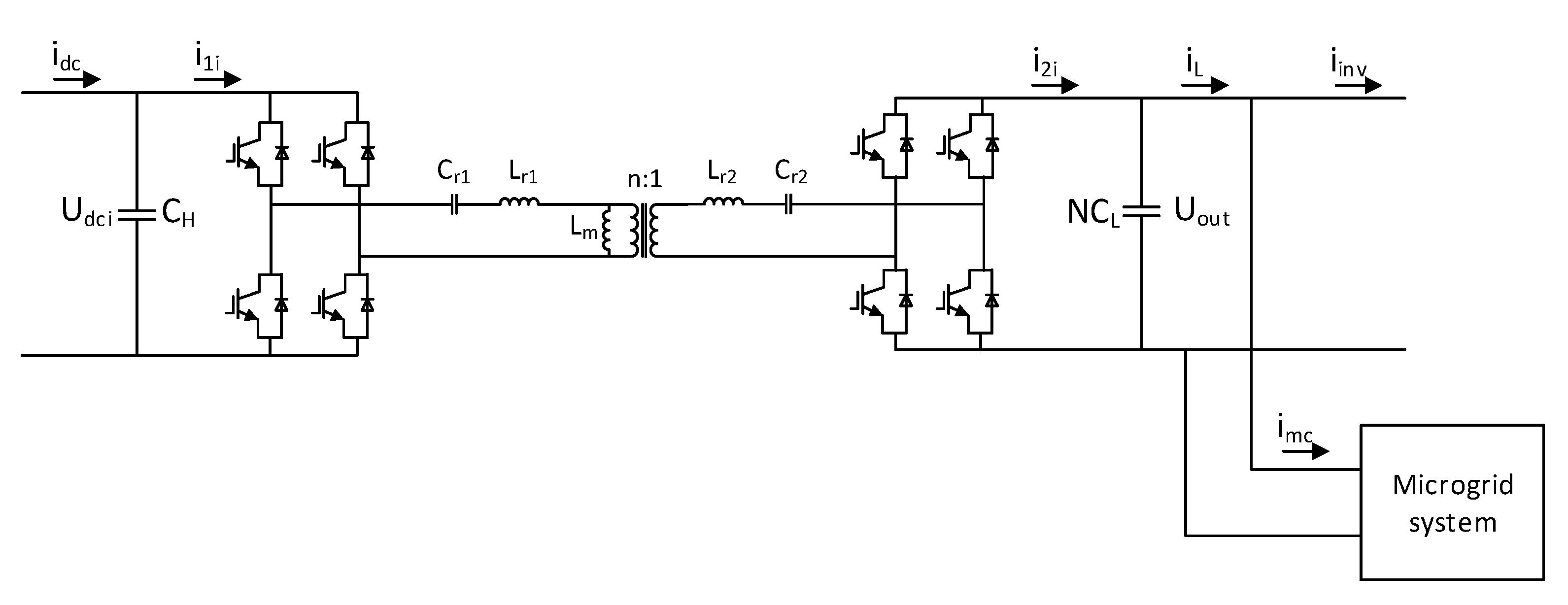
The topology of a single submodule of the CLLC resonant converter is shown in Figure 4, where i dc is the input current of the HVDC link; U dci and U out are the input and output DC voltages of the submodule; i 1 i and i 2 i are the input and output currents; i L i is the outlet current of submodule i, and i L is the outlet current of the overall input-series–output-parallel (ISOP) CLLC resonant converter; C r 1 , L r 1 and C r 2 , L r 2 are the resonant capacitors and inductors on the primary and secondary sides; L m is the magnetic inductor, which can be integrated inside the HFT; n is the transformation ratio of the HFT; NC L represents the equivalent parallel capacitance of the LVDC link; and i inv and i mc are the input currents of the output stage and local DC microgrid.
Under single-phase-shift control, the transmission power of the CLLC resonant converter can be obtained as:
P CLLCi = 8 nU dci U out π 2 | Z eqi | cos ( φ i + θ i )
where P CLLCi is the transmission power of submodule i; φ i is the phase shift angle between two H-bridges; and | Z eqi | and θ i are the magnitude and phase of the equivalent impedance Z eqi , which can be calculated as:
Z eqi = Z 1 ( Z m + Z 2 + 8 π 2 Z loadi ) + Z m ( Z 2 + 8 π 2 Z loadi ) Z m = | Z eqi | θ i
where Z 1 , Z 2 , Z m , and Z loadi represent the primary-side LC resonant impedance, secondary-side resonant impedance, the excitation impedance of the HFT, and load impedance (all equivalent to the primary side). From Equations (2) and (3), the input and output currents of the isolation stage can be calculated as:
{ i 1 i = 8 nU out π 2 | Z eqi | cos ( φ i + θ i ) i 2 i = 8 nU dci π 2 | Z eqi | cos ( φ i + θ i )
and the dynamic equation of output voltage can be expressed as:
NC L dU out dt = i = 1 N i 2 i     i inv     i mc = i 2 i L
where i 2 is the sum of the output currents of N CLLC submodules. Without loss of generality, the voltage and power balance control between the CLLC submodules are not considered in this paper, that is to say, the operating variables of N submodules are assumed to be the same, so the ISOP CLLC resonant converter can be equivalent to one submodule.

2.2. Problems Existing in the Independent Control Strategy

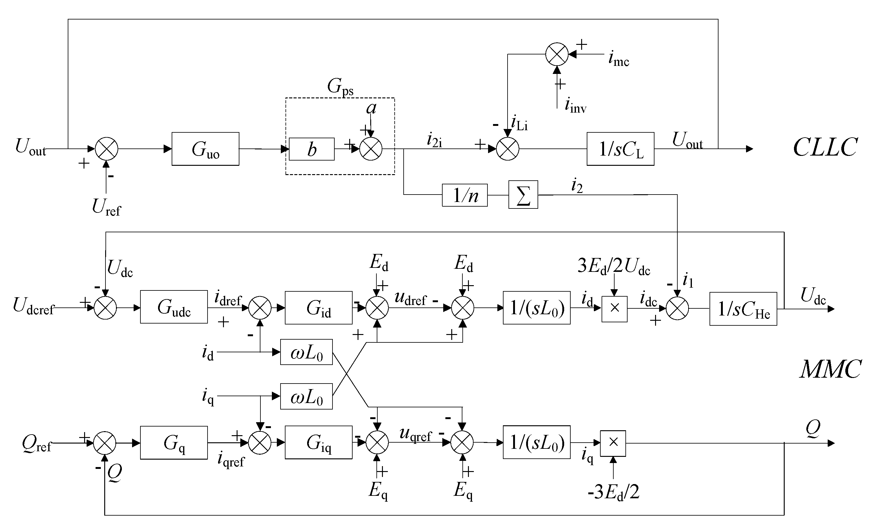
In the three-stage independent control, the input-stage MMC adopts voltage and current double-loop control to maintain the HVDC bus voltage and adjust the power factor on the distribution grid side; the CLLC adopts single-phase-shift control to regulate the parallel output voltage of the isolation stage. The control diagram is shown in Figure 5. In this figure, Q is the reactive power of the distribution network; G udc , G id , G q , and G iq represent the double-loop controller functions of the MMC; and G uo is the controller function for the CLLC, which adopts single voltage-loop control, so no high-precision current sensor is needed. The part inside the dotted box represents the relation between φ i and i 2 i , which has been given by the second line of Equation (4). It is obvious that G ps is a nonlinear function, since the CLLC usually works near the resonant frequency point, which means that θ i 0. Therefore, a linear approximation for G ps is carried out in this paper. The approximate expression after linearization is as follows ( 0   <   φ   <   π ):
{ i 2 i = a + b φ i a = 8 nU dc π 2 | Z eqi | b   16 nU dc π 3 | Z eqi |
As mentioned previously, the topology of the grid-connected DC microgrid system is shown in Figure 3. A boost chopper circuit is usually adopted as the interfacing converter for PV to realize the maximum power point tracking (MPPT) control [23,24]. The topology and control diagram are shown in Figure 6a,b. For the energy storage system, which includes batteries and super capacitors, the interface converter must realize a bidirectional power transmission, so the current reversible chopper circuit is usually used. Common control methods include constant DC voltage control and voltage droop control. The topology and control diagram are shown in Figure 6c,d.
In normal operation, the SST acts as the balance node of the system to provide the voltage and frequency support, the DGs output at maximum power, and the energy storage equipment responses to the control-center command. In this case, fast and continuous fluctuations of the distributed power output will be sufficiently compensated in real time by the SST. It can be seen from Figure 5 that the output current of the microgrid is the interference to the CLLC control loop, which means that the change of i Li leads to the fluctuation of i 2 i and U out . The current of the CLLC port is the interference to the MMC active power control loop, which means that the change of i 2 i will further lead to the fluctuation of U dc . In addition, the difference of power response speed between the MMC and CLLC resonant converter will aggravate the situation. From Figure 5, the transfer function of the CLLC output DC current i 2 i to its load current i Li can be obtained. Since the CLLC can be equivalent to one submodule, so the transfer function of i 2 to i L will be the same as i 2 i to i Li , as illustrated in Equation (7):
i 2 i L = G uo G ps G uo G ps sNC L
Similarly, the transfer function of the MMC output DC current i dc to the CLLC input current i 1 can be expressed as:
i dc i 1 = 3 E d G udc G idd 3 E d G udc G idd 2 U dc C He
where G idd is the transfer function of the grid connected current in the d-axis, and its expression is:
G idd = i d i dref = G id   G id + L 0 s
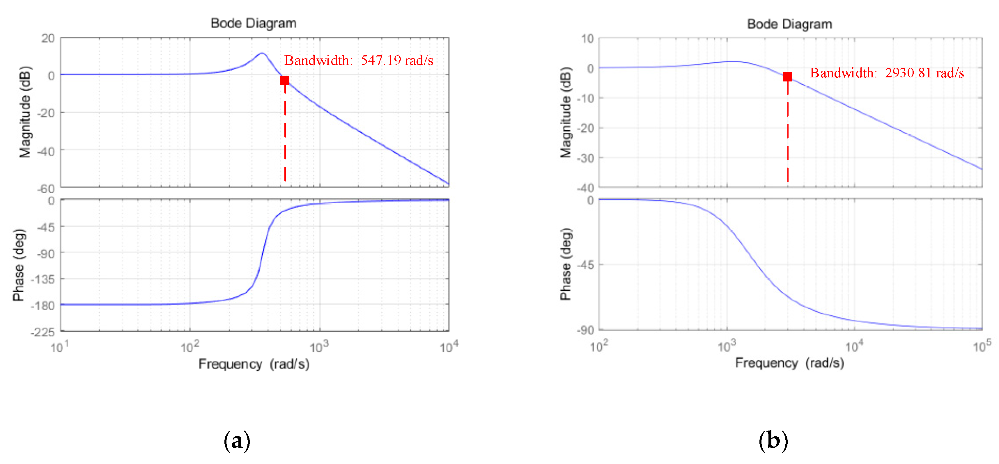
According to the control parameters listed in Table 1 and the system hardware simulation parameters listed in Table 2 in Section 4, the current response Bode diagrams of HVDC and LVDC links can be drawn, as shown in Figure 7. In Table 1, the proportion and integral parameters of PI controllers are distinguished by the subscripts P and I. For example, K uo   =   K Puo   +   K Iuo . It can be seen from Figure 7 that the closed-loop bandwidth of i 2 to i L is 2930.81 rad/s, which is much larger than the 547.19 rad/s of i dc to i 1 . It indicates that the power adjustment speed of the CLLC is much faster than that of the MMC. Therefore, when the output power of the microgrid fluctuates dramatically, such as switching from absorbing electricity to generating electricity to the distribution network, the power response speed of the CLLC is much faster than that of the MMC.
According to the dynamic Equation (1), the capacitance voltage fluctuation of the HVDC link depends on the current difference between its two sides, that is, the capacitance voltage itself is determined by the difference of the current integral value:
U dc = 1 C He   i dc dt 1 C He   i 1 dt

3. Hierarchical Coordinative Control Strategy Design

3.1. The Hierarchical Coordinative Control for the SST-Based DC Microgrid System

With respect to the problems existing in the independent control, a hierarchical coordinative control strategy for the SST and microgrid composite system is proposed. In general, the hierarchical coordinative control mitigates the local microgrid’s external power fluctuation and realizes a joint action of the MMC and the CLLC during the dynamic process. The comparison of control logic between independent control and coordinative control is shown in Figure 8.
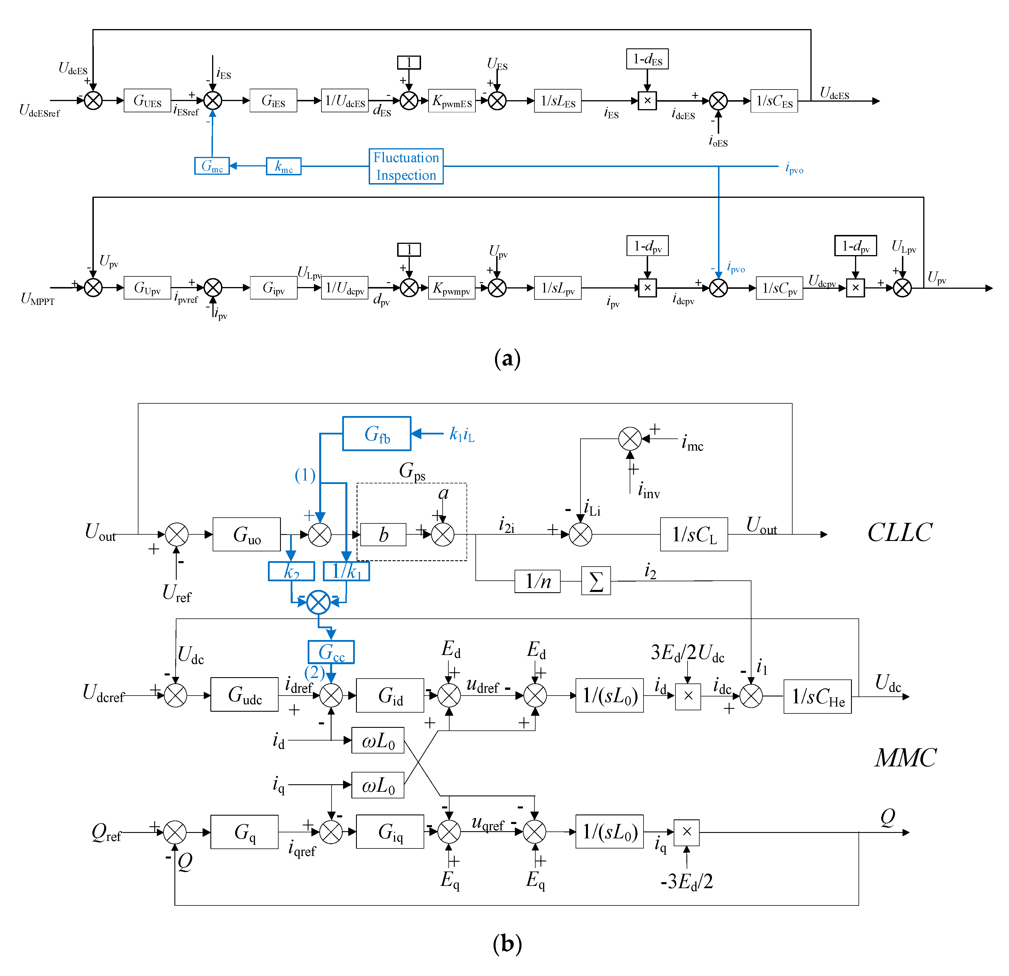
The overall coordinative control diagram is shown in Figure 9. This novel control strategy contains two layers: the microgrid layer and the SST layer. In Figure 8a, G UES and G IES represent the ESS double-loop PI controller; G UPV and G IPV are the control functions for the PV controller; K PWMES and K PWMPV are the equivalent gain of the pulse width modulation (PWM) links for ESS and PV, respectively ( K PWMES     U dcES , K PWMPV     U dcPV ); and d ES and d PV are the equivalent duty cycles. The meaning of the remaining parameters of Figure 9 has been given in Figure 6.
In the microgrid layer control, the additional control branch feeds the variation of PV outlet current back to the inner current loop of super capacitors inside the ESS, giving full play to the fast regulation capability of super capacitors. Although mechanical and battery energy storage systems are still the key elements in system operation, super capacitors nowadays are drawing an increasing interest [25], due to the advantages of high efficiency and high power density [26]. This paper adopts a hybrid energy storage device combining super capacitors and batteries, as discussed in [27,28,29]. In the additional control branch, k mc is the coordinative control coefficient, which reflects the compensation degree of PV output fluctuation by the ESS. G mc is the coordinative transfer function, and the fluctuation inspection section represents the instruction-receiving and triggering module.
In the SST layer control, the control branch 1 feeds the load current of the CLLC forward to the inner current loop as a new control variable to improve the dynamic current response speed of the CLLC stage. The additional control branch 2 not only feeds the output of the CLLC voltage controller back to the inner loop of the MMC, bringing the two parts of the SST together to complete the task of LVDC bus voltage control, but also feeds the CLLC load current back, to eliminate the influence of the CLLC current fluctuation on the HVDC link at the same time. Similar to the microgrid layer control, k 1 and k 2 are additional control coefficients; G fb and G cc are the corresponding transfer functions. The expressions are as follows:
{ G mc   =   G iES + sL ES G iES G fb = 1 b G cc = 2 bU dc ( G id + sL 0 ) 3 nE d G id

3.2. Comparative Analysis of Microgrid Power Fluctuation Response of the DC Link

From Figure 4, Figure 5 and Figure 9b, the voltage response functions of the SST DC links to the CLLC load current i L under the independent control can be given in Equation (12), where L 0 is equal to L s + L a   2 and is the equivalent inductance on the AC side of the MMC.
{ U out I L = 1 bG uo NC L s U dc I L = bG uo n ( bG uo NC L s ) ( sC He + 3 E d G udc G idd 2 U dc )
Since the independent control is only for three-stage SST converters, the proposed microgrid layer control is not considered in the comparative analysis. From Figure 9b, the corresponding disturbance response functions under the SST-layer coordinative control can be expressed as:
{ U out I L = 1 k 1 bG uo NC L s U dc I L = ( 1 k 1 ) ( bk 2 G uo NC L s ) n ( bG uo NC L s ) ( sC He + 3 E d G udc G idd 2 U dc )
As can be seen from Equations (12) and (13), the additional control branches change the numerator of the disturbance response functions. If the value of the control parameter k 1 is close to 1, the dynamic voltage fluctuation problem of HVDC and LVDC buses caused by microgrid output power swing can be completely solved in theory. The coefficient k 2 aims to improve the dynamic power tracking speed difference between the MMC and the CLLC, so as to realize the joint regulation of these two stages in the dynamic process. Although this effect is not clearly reflected in the above formulas, it can be seen from the disturbance transfer function of HVDC bus voltage to the CLLC input current i 1 before and after the introduction of the k 2 branch, as shown in Equation (14). The introduction of k 2 improves the tracking ability of the MMC to current i 1 , and the whole coordinative control branch (2) does not need additional sensors.
{ U dc I 1 = 1 sC He + 3 E d G udc G idd 2 U dc U dc I 1 = 1 k 2 sC He + 3 E d G udc G idd 2 U dc
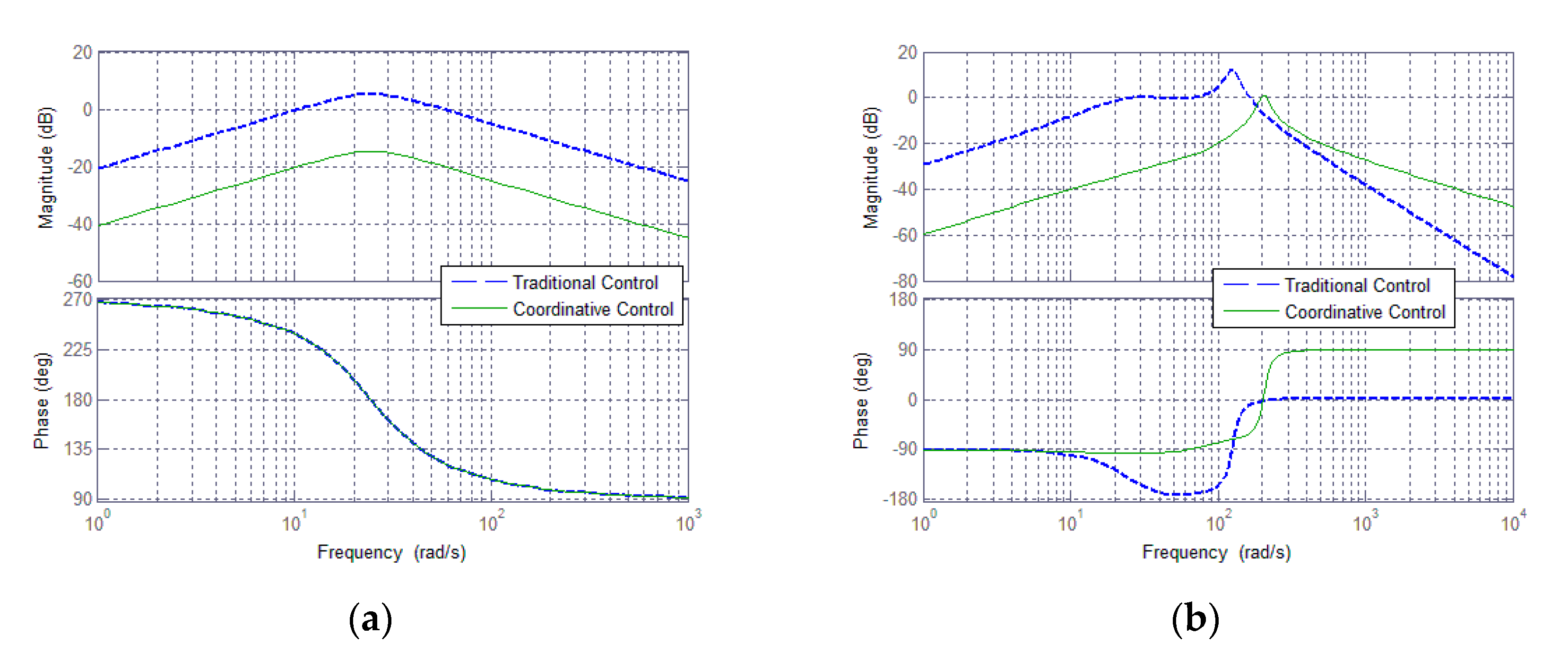
The system simulation parameters are shown in Table 2. According to Equations (12) and (13), the Bode diagrams of the disturbance response functions can be obtained, as shown in Figure 10. From this figure, it can be seen that the coordinative control strategy proposed in this paper can significantly improve the low-frequency amplitude gain, indicating that this coordinative strategy has a better suppression for the DC bus voltage fluctuating during a same dynamic process. The Bode diagram of Equation (14) is similar to that of Equation (12), since the coefficient k 2 acts on the numerator, and so it is not repeated here.

4. Simulation Results

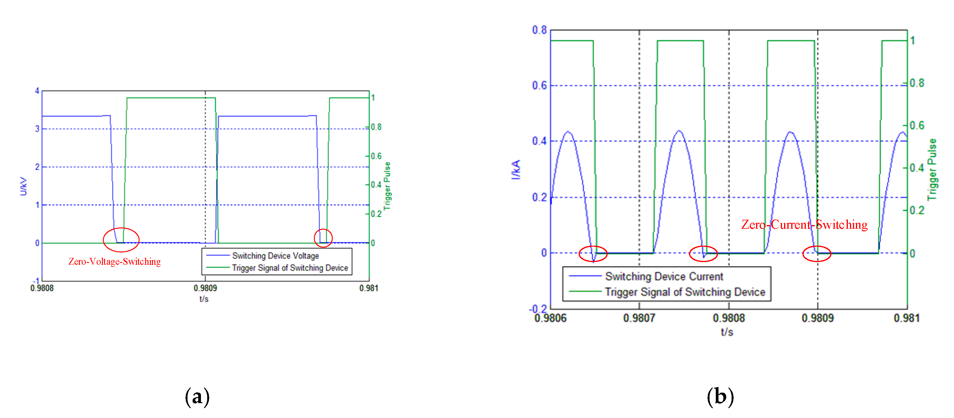
The model of the SST-based DC microgrid system, as shown in Figure 3, is built by PSCAD/EMTDC to verify the proposed coordinative control. PSCAD/EMTDC is a professional electromagnetic transient simulation software, which is also suitable for power electronics system simulations. The simulation parameters are listed in Table 2. The rated capacity of the SST is 1.5 MVA, and the distribution grid keeps running under unity power factor. In steady-state operation, the output stage of the SST has a 1 MW three-phase unbalanced load. At this time, the working waveform of the CLLC is shown in Figure 11. It can be seen that the voltage zero-crossing point of the primary-side switch is ahead of the turn-on signal, and the current zero-crossing point of the secondary-side switch is ahead of the turn-off signal, thereby reducing switching losses. Figure 12 shows the efficiency curve of the CLLC resonant converter under different load conditions. It can be seen that, when the power is transmitted bidirectionally, the half-load efficiency can reach above 97%, and the efficiency can reach above 98% at a rated power of 1.5 MW.
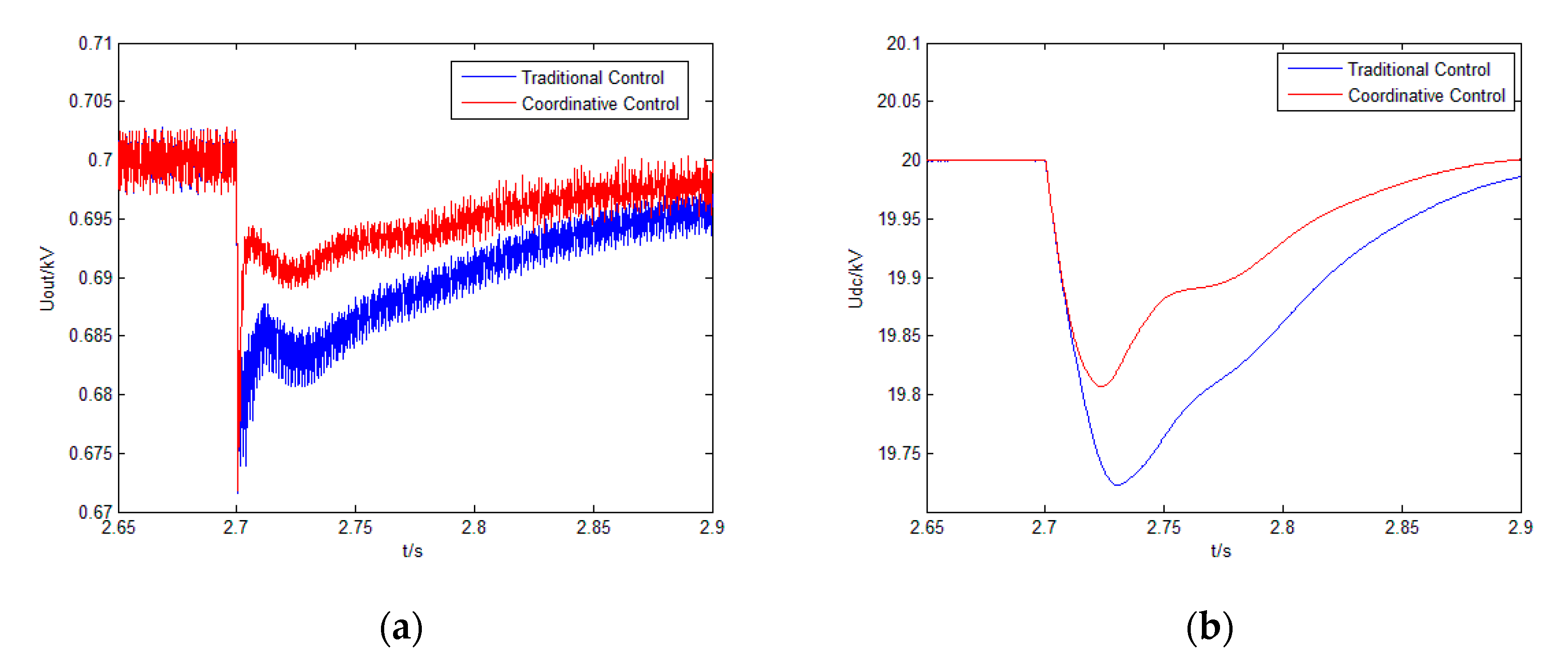
At 1.5 s, the DC microgrid is connected to the system, the PV output is 0.3 MW, and the DC load is 0.2 MW. Starting from 2.7 s, the output power of the PV supply in the microgrid fluctuates continuously in a wide range, and the variation rule is 0.3 MW–2 MW–0.3 MW–2 MW. In this process, the power flow direction of the SST will change frequently under independent control. Figure 13 shows the response of the LVDC and HVDC bus voltages. It can be seen from the comparison that the hierarchical coordinative control strategy proposed in this paper can quickly stabilize the bus voltage and greatly improve the power quality in the dynamic process. Using traditional control strategy, the maximum transient voltage changes of the LVDC and HVDC links are about 47 V and 580 V, respectively. However, under the proposed coordinative control strategy, the DC bus voltage has almost no fluctuation.
The microgrid layer control utilizes the fast power response of super capacitors to smooth the power fluctuation of the DGs. The current waveform of the SST during power fluctuation is shown in Figure 14. It can be seen that the compensated DG output current does not cause frequent fluctuations in the SST power transmission direction, and the change of SST current is relatively smooth.
It is worth noting that the proposed coordinative control strategy can actually be applied to mitigate dynamic voltage fluctuation conditions. For example, when the system detects a fault in the DC microgrid and trips it off at 2.7 s, the corresponding voltage response is shown in Figure 15. Before removal, the output of the PV power supply is 1 MW. It can be seen from the figure that the SST layer coordinative control at this time can rapidly compensate for the power shortage and restore the DC link voltages to the given value more quickly.
When the control strategy shown in Figure 9a is slightly changed to make the super capacitors dynamically compensate for the input current of the output-stage inverter in the island switching process, i.e., i inv in Figure 4, the coordinative control can also smooth the island switching process. The voltage waveform of the LVDC bus under this condition is shown in Figure 16. Although only the microgrid layer coordinative control plays a role at this time, the bus voltage fluctuation could still be suppressed by a considerable extent. Under the microgrid layer coordinative control, the maximum voltage sag is about 37 V. While under the independent control, the maximum voltage sag is about 90 V, and the voltage needs longer time to recover.
The strategies to improve the SST power quality in previous studies are mostly considering the power-side disturbances [30] and load fluctuations [31]. However, power-side disturbances and load fluctuations do not directly act on the DC buses of the SST, and they can always be isolated by adjacent inverters. In both cases, independent control strategies can maintain good power quality. At present, there are few researches on the power quality problem of SST DC ports caused by the output fluctuation of microgrid.

5. Conclusions

In this paper, the topology of the SST is improved, and a hierarchical coordinative control strategy for an SST integrated DC microgrid system is proposed to solve the dynamic voltage quality problem of SST DC ports caused by the random and intermittent characteristics of distributed generators. Through mathematical analysis and simulation, conclusions can be drawn as follows:
(1)
At present, the main factors affecting the practical application of SSTs are high cost and low energy transmission efficiency. The adopted input-stage MMC instead of cascaded H-bridge can significantly reduce the required number of power electronic switches and high-frequency transformers in the SST, thus reducing the system cost. As for the isolation stage that accounts primarily for SST power losses, the efficiency of the CLLC resonant converter adopted in this paper can reach above 98% at rated power, which is greatly improved, compared with the DAB converter, whose efficiency is only about 90%.
(2)
Under the independent control, the power response speed of the SST is slow, and the output fluctuation of the microgrid cannot be compensated quickly and timely, bringing serious dynamic voltage stability problems for the DC link voltages. The hierarchical coordinative control strategy proposed in this paper can not only improve the external power characteristics of the DC microgrid, but also realize a coordinated action between the input stage and isolation stage of the SST, which can greatly suppress the voltage fluctuation of the HVDC and LVDC bus.
(3)
The coordinative control strategy is not only applicable to the microgrid output fluctuation situation, but also effective to other transient conditions, such as the removal of the microgrid under fault, and the island switching process.

Author Contributions

conceptualization: Z.L. and T.Z.; methodology: Z.L. and Y.W.; software: Z.L., Y.W., and C.Y.; validation: Z.L.; formal analysis: Z.L.; writing—original draft preparation: Z.L., Y.W., and C.Y.; writing—review and editing: Z.L., C.Y., and T.Z.; visualization: Z.L. and C.Y.; supervision: T.Z.; project administration: T.Z.; funding acquisition: T.Z. All authors have read and agreed to the published version of the manuscript.

Funding

This research was funded by the Key Research and Development Program of Shaanxi Province, grant number 2019ZDLGY18-06.

Conflicts of Interest

The authors declare that there are no conflicts of interest.

Abbreviations

CHBCascaded H-bridge
DABDual active bridge
DABCIDual active bridge cascaded with inverter
DGDistributed generation
ESSEnergy storage system
FECFront-end converter
HFTHigh frequency transformer
HVDCHigh-voltage direct current
ISOP Input-series output-parallel
LVDCLow-voltage direct current
MMCModular multilevel converter
MPPTMaximum power point tracking
PVPhotovoltaic
PWMPulse width modulation
SSTSolid state transformer

References

  1. Tu, C.; Xiao, F.; Lan, Z.; Shuai, Z. Research of the high supply voltage quality control for solid-state transformer. IET Power Electron. 2018, 11, 1788–1795. [Google Scholar] [CrossRef]
  2. Yun, C.-G.; Cho, Y. Active Hybrid Solid State Transformer Based on Multi-Level Converter Using SiC MOSFET. Energies 2019, 12, 66. [Google Scholar] [CrossRef] [Green Version]
  3. Miao, J.; Zhang, N.; Kang, C.; Wang, J.; Wang, Y.; Xia, Q. Steady-State Power Flow Model of Energy Router Embedded AC Network and Its Application in Optimizing Power System Operation. IEEE Trans. Smart Grid 2018, 9, 4828–4837. [Google Scholar] [CrossRef]
  4. Anand, S.; Fernandes, B.G.; Guerrero, J. Distributed Control to Ensure Proportional Load Sharing and Improve Voltage Regulation in Low-Voltage DC Microgrids. IEEE Trans. Power Electron. 2013, 28, 1900–1913. [Google Scholar] [CrossRef] [Green Version]
  5. Xiao, W.; Ge, B.; Zang, T.; Liu, Y.; Zhang, Z.; Yang, F. Management system research of large-scale new energy development based on energy internet. In Proceedings of the 2017 IEEE Conference on Energy Internet and Energy System Integration (EI2), Beijing, China, 26–28 November 2017; pp. 1–6. [Google Scholar]
  6. Wang, R.; Sun, Q.; Cheng, Q.; Ma, D. The Stability Analysis of a Multi-Port Single-Phase Solid-State Transformer in the Electromagnetic Timescale. Energies 2018, 11, 2250. [Google Scholar] [CrossRef] [Green Version]
  7. Li, Z.; Gao, F.; Zhao, C.; Wang, Z.; Zhang, H.; Wang, P.; Li, Y. Research Review of Power Electronic Transformer Technologies. Proc. CSEE 2018, 38, 1274–1289. [Google Scholar]
  8. Wang, D.; Tian, J.; Mao, C.; Lu, J.; Duan, Y.; Qiu, J.; Cai, H. A 10-kV/400-V 500-kVA Electronic Power Transformer. IEEE Trans. Ind. Electron. 2016, 63, 6653–6663. [Google Scholar] [CrossRef]
  9. Gao, F.; Li, Z.; Wang, P.; Xu, F.; Chu, Z.; Sun, Z.; Li, Y. Prototype of smart energy router for distribution DC grid. In Proceedings of the 17th European Conference on Power Electronics and Applications (EPE’15 ECCE-Europe), Geneva, Switzerland, 8–10 September 2015; pp. 1–9. [Google Scholar]
  10. Chen, W.; Rong, P.; Lu, Z. Snubberless Bidirectional DC–DC Converter With New CLLC Resonant Tank Featuring Minimized Switching Loss. IEEE Trans. Ind. Electron. 2010, 57, 3075–3086. [Google Scholar] [CrossRef]
  11. Jung, J.; Kim, H.; Kim, J.; Ryu, M.; Baek, J. High efficiency bidirectional LLC resonant converter for 380V DC power distribution system using digital control scheme. In Proceedings of the 2012 Twenty-Seventh Annual IEEE Applied Power Electronics Conference and Exposition (APEC), Orlando, FL, USA, 5–9 February 2012; pp. 532–538. [Google Scholar]
  12. Li, D.; Zhu, Z.Q. A Novel Integrated Power Quality Controller for Microgrid. IEEE Trans. Ind. Electron. 2015, 62, 2848–2858. [Google Scholar] [CrossRef]
  13. Pradhan, M.; Mishra, M.K. Dual P-Q Theory Based Energy-Optimized Dynamic Voltage Restorer for Power Quality Improvement in a Distribution System. IEEE Trans. Ind. Electron. 2019, 66, 2946–2955. [Google Scholar] [CrossRef]
  14. Rauf, A.M.; Khadkikar, V. An Enhanced Voltage Sag Compensation Scheme for Dynamic Voltage Restorer. IEEE Trans. Ind. Electron. 2015, 62, 2683–2692. [Google Scholar] [CrossRef]
  15. Madhusoodhanan, S.; Tripathi, A.; Patel, D.; Mainali, K.; Kadavelugu, A.; Hazra, S.; Bhattacharya, S.; Hatua, K. Solid-State Transformer and MV Grid Tie Applications Enabled by 15 kV SiC IGBTs and 10 kV SiC MOSFETs Based Multilevel Converters. IEEE Trans. Ind. Appl. 2015, 51, 3343–3360. [Google Scholar] [CrossRef]
  16. Vasiladiotis, M.; Rufer, A. A Modular Multiport Power Electronic Transformer With Integrated Split Battery Energy Storage for Versatile Ultrafast EV Charging Stations. IEEE Trans. Ind. Electron. 2015, 62, 3213–3222. [Google Scholar] [CrossRef]
  17. Rahman, M.A.; Islam, M.R.; Muttaqi, K.M.; Sutanto, D.A. Modeling and Control of SiC-Based High-Frequency Magnetic Linked Converter for Next Generation Solid State Transformers. IEEE Trans. Energy Convers. 2019, 35, 549–559. [Google Scholar] [CrossRef]
  18. Zhao, T.; Wang, G.; Zeng, J.; Dutta, S.; Bhattacharya, S.; Huang, A.Q. Voltage and power balance control for a cascaded multilevel solid state transformer. In Proceedings of the 2010 Twenty-Fifth Annual IEEE Applied Power Electronics Conference and Exposition (APEC), Palm Springs, CA, USA, 21–25 February 2010; pp. 761–767. [Google Scholar]
  19. Tian, Y.; Chen, Z.; Deng, F.; Sun, X.; Hu, Y. Active Power and DC Voltage Coordinative Control for Cascaded DC–AC Converter With Bidirectional Power Application. IEEE Trans. Power Electron. 2015, 30, 5911–5925. [Google Scholar] [CrossRef]
  20. Ge, J.; Zhao, Z.; Yuan, L.; Lu, T. Energy Feed-Forward and Direct Feed-Forward Control for Solid-State Transformer. IEEE Trans. Power Electron. 2015, 30, 4042–4047. [Google Scholar] [CrossRef]
  21. Rahman, M.A.; Islam, M.R.; Muttaqi, K.M.; Sutanto, D. Data driven coordinated control of converters in a smart solid state transformer for reliable and automated distribution grids. IEEE Trans. Ind. Appl. 2020, 56, 4532–4542. [Google Scholar] [CrossRef]
  22. Briz, F.; Lopez, M.; Rodriguez, A.; Arias, M. Modular power electronic transformers: Modular multilevel converter versus cascaded H-bridge solutions. IEEE Trans. Ind. Electron. 2016, 10, 4587–4597. [Google Scholar] [CrossRef]
  23. Wu, L.; Zhao, Z.; Liu, J. A Single-Stage Three-Phase Grid-Connected Photovoltaic System With Modified MPPT Method and Reactive Power Compensation. IEEE Trans. Energy Convers. 2007, 22, 881–886. [Google Scholar]
  24. Moon, S.; Yoon, S.; Park, J. A New Low-Cost Centralized MPPT Controller System for Multiply Distributed Photovoltaic Power Conditioning Modules. IEEE Trans. Smart Grid 2015, 6, 2649–2658. [Google Scholar] [CrossRef]
  25. Dougal, R.A.; Liu, S.; White, R.E. Power and life extension of battery-super capacitor hybrids. IEEE Trans. Compon. Packag. Technol. 2002, 25, 120–131. [Google Scholar] [CrossRef] [Green Version]
  26. Ostadi, A.; Kazerani, M. A Comparative Analysis of Optimal Sizing of Battery-Only, Super capacitor-Only, and Battery–Super capacitor Hybrid Energy Storage Systems for a City Bus. IEEE Trans. Veh. Technol. 2015, 64, 4449–4460. [Google Scholar] [CrossRef]
  27. Zheng, J.P.; Jow, T.R.; Ding, M.S. Hybrid power sources for pulsed current applications. IEEE Trans. Aerosp. Electron. Syst. 2001, 37, 288–292. [Google Scholar] [CrossRef]
  28. Gao, L.; Dougal, R.A.; Liu, S. Power enhancement of an actively controlled battery/super capacitor hybrid. IEEE Trans. Power Electron. 2005, 20, 236–243. [Google Scholar] [CrossRef]
  29. Camara, M.B.; Gualous, H.; Gustin, F.; Berthon, A. Design and New Control of DC/DC Converters to Share Energy Between Supercapacitors and Batteries in Hybrid Vehicles. IEEE Trans. Veh. Technol. 2008, 57, 2721–2735. [Google Scholar] [CrossRef]
  30. Wang, J.; Gu, B.; Duan, Q.; Ma, C.; Ji, B.; You, J. Control strategy of solid state power electronic transformer under voltage disturbance conditions. In Proceedings of the IECON 2015-41st Annual Conference of the IEEE Industrial Electronics Society, Yokohama, Japan, 9–12 November 2015; pp. 003081–003085. [Google Scholar]
  31. Rashidi, M.; Bani-Ahmed, A.; Nasiri, A. Application of a multi-port solid state transformer for volt-var control in distribution systems. In Proceedings of the IEEE Power & Energy Society General Meeting, Chicago, IL, USA, 16–20 July 2017; pp. 1–4. [Google Scholar]
Figure 1. Structure of a three-stage solid state transformer.
Applsci 10 06853 g001
Figure 2. Topology of the solid state transformer (SST).
Applsci 10 06853 g002
Figure 3. Topology of a DC microgrid system.
Applsci 10 06853 g003
Figure 4. The submodule topology of the CLLC resonant converter.
Applsci 10 06853 g004
Figure 5. The independent control strategy of the SST.
Applsci 10 06853 g005
Figure 6. Topology and control strategy of the photovoltaic (PV) and energy storage system (ESS): (a) the interface converter for the PV; (b) the maximum power point tracking (MPPT) control diagram for the PV; (c) The interface converter for the ESS; (d) The control strategy for the ESS.
Applsci 10 06853 g006
Figure 7. Current response Bode diagrams under independent control: (a) current response of the high-voltage DC (HVDC) link; (b) current response of the low-voltage DC (LVDC) link.
Applsci 10 06853 g007
Figure 8. Control logic of the independent control and proposed coordinative control.
Applsci 10 06853 g008
Figure 9. The hierarchical coordinative control diagram: (a) the microgrid layer control; (b) the SST layer control.
Applsci 10 06853 g009
Figure 10. The voltage response Bode diagrams of the HVDC and LVDC links to the CLLC load current: (a) the LVDC bus voltage response; (b) the HVDC bus voltage response.
Applsci 10 06853 g010
Figure 11. The steady-state working waveform of the CLLC: (a) the zero-voltage-switching waveform of the primary-side switching device; (b) the zero-current-switching waveform of the secondary-side switching device.
Applsci 10 06853 g011
Figure 12. Efficiency curve of the CLLC under different load conditions.
Applsci 10 06853 g012
Figure 13. The comparison of voltage response under continuous power fluctuation: (a) the LVDC bus voltage response; (b) the HVDC bus voltage response.
Applsci 10 06853 g013
Figure 14. The current waveform of the SST under continuous power fluctuation: (a) the distribution network current; (b) the HVDC-link current; (c) the LVDC-link current.
Applsci 10 06853 g014
Figure 15. The comparison of voltage response after the DC microgrid is tripped off: (a) the LVDC bus voltage response; (b) the HVDC bus voltage response.
Applsci 10 06853 g015
Figure 16. The comparison of voltage response during the island switching process.
Applsci 10 06853 g016
Table 1. Parameters of the solid state transformer controller.
VariablesValueVariablesValue
K Puo 0.04 K Iuo 40
K Pudc 4 K Idc 100
K Pid 0.5 K Iid 50
Table 2. The simulation parameters of the SST-based DC microgrid system.
Variable DescriptionValue
Distribution network voltage level10 kV
Distribution grid side filter inductor ( L s )10 mH
Three-phase arm inductance of MMC ( L a )20 mH
Number of submodules of MMC and CLLC (N)6
Reference value of HVDC voltage ( U dcref )20 kV
Primary-side voltage of CLLC submodule ( U dci )3.33 kV
Secondary-side voltage of CLLC submodule ( U out )700 V
Turns ratio of HFT (n)4.76:1
HVDC-link series capacitance ( C H )3000 uF
LVDC-link shunt capacitance ( C L )3000 uF
Primary-side resonant inductance ( L r 1 )15 uH
Primary-side resonant capacitance ( C r 1 )19 uF
Secondary-side resonant inductance ( L r 2 )0.216 uH
Primary-side resonant capacitance ( C r 2 )1319.42 uF
CLLC excitation inductance ( L m )2300 uH
Coordinative control coefficient K 1 0.9
Control coefficient K 2 0.9