Article

Effect of the Surface Roughness of Tungsten on the Sputtering Yield under Helium Irradiation: A Molecular Dynamics Study

Department of Nuclear Engineering, Kyung Hee University, Yongin-si 17104, Korea
*
Author to whom correspondence should be addressed.
Metals 2021, 11(10), 1532; https://doi.org/10.3390/met11101532
Submission received: 30 July 2021 / Revised: 15 September 2021 / Accepted: 24 September 2021 / Published: 26 September 2021
(This article belongs to the Special Issue Modeling and Microstructure Evolution of Solid State Materials)

Abstract

:
Sputtering in a divertor is one of the key phenomena that affects plasma purity and temperature. In previous experimental studies, the term sputtering yield has been used to refer to net sputtering yield, which is defined as the difference between primary sputtering yield and re-deposition. Our simulations using molecular dynamics have confirmed that both primary sputtering yield and re-deposition are affected by particle curvature. In this study, the effect of particle curvature on the net sputtering yield was quantitatively evaluated, the results were compared to existing experimental studies, and the discrepancies with experimental results were discussed.

1. Introduction

A divertor is an armor component that maintains the integrity of fusion reactors from the irradiation of high-temperature plasma. He ions and neutrons are produced as a result of fusion reactions between deuterium and tritium in ultra-high temperature plasma [1,2]. The irradiation of the He ions and neutrons degrades the properties of materials; therefore, the integrity of the components is damaged [3,4].
Sputtering refers to the phenomenon in which an ion is accelerated and collides with a solid material, causing the atoms that make up the material to bounce outward [5,6]. The sputtering introduces particles into the plasma, which reduces its purity and lowers its temperature; as a result, the high temperature of the plasma can no longer be maintained [3,7]. Therefore, a divertor must be composed of materials which have a low sputtering yield [4,6]. Since the sputtering yield of tungsten is considerably low amongst all high-temperature materials, tungsten has been considered to be a potential material for use in this application [8,9,10,11]. Although tungsten has several disadvantages, efforts have been made to overcome these disadvantages and use it as a divertor material [12,13,14,15].
Although the sputtering yield of tungsten is lower than that of other high-temperature materials, it still needs to be further reduced in order to maintain plasma at a high temperature for a long time. Intensive investigations have been conducted with the aim to lower the sputtering yield of a divertor composed of tungsten [16,17]. In order to manufacture a divertor, tungsten powder is heat-treated at a high temperature under high pressure [18]. Various studies have been conducted to reduce the sputtering yield by controlling the roughness of the tungsten powder [14,15]. In previous experimental studies, the sputtering yield increases as the roughness of the surface increases [15,19,20], and it was hypothesized that the trend was caused by the re-deposition process. Re-deposition refers to a phenomenon in which sputtered tungsten atoms are re-deposited on convex tungsten hills, as shown in Figure 1. In this study, the above hypothesis was examined by molecular dynamics simulations, which have frequently been used to simulate plasma–material interaction [21,22,23].

2. Simulation Method

LAMMPS is an MD package with features that make it easy to configure the desired system. We utilized the interatomic potentials between the W-W, W-He, and He-He atoms studied by N. Juslin et al. [21,24]. According to N. Juslin et al., the interatomic potential of W-He is given as the following equation: [24]
V ( r i j ) = Z B L 10 eV , r i j r 1 a 5 r i j 5 + a 4 r i j 4 + a 3 r i j 3 + a 2 r i j 2 + a 1 r i j + a 0 , r 1 r i j r 2 V A T p o t , r i j r 2
ZBL is the Ziegler–Biersack–Littmark potential [23] and V A T p o t is the Ackland–Thetford tungsten potential [22]. According to N. Juslin et al., if the ZBL potential is reduced by 10 eV, it will be similar to the AT potential in a short range [24]. Therefore, the interatomic potential in a short range is expressed as shown in Equation (1). The interatomic potential of He-He is given as the following equation [21]:
v ( r ) = A e x p ( α r β r 6 ) 0.869 ( r 2 + a 2 ) 3 1 + 2.709 + 3 a 2 r 2 + a 2
In molecular dynamics simulation, the re-deposition phenomenon was captured by estimating the positions of W atoms over time according to the laws of classical mechanics without any prior assumptions about the re-deposition process.
To compare the roughness effect on the net sputtering yield, we set three geometries, as shown in Figure 2. Geometry 1 is a cuboid shape. Using geometry 1 as a common part, we merged a dome shape with geometries 2 and 3. We cut off some of the spheres with radii 9.4956 nm and 4.7478 nm, respectively, and combined them with geometry 1. Thus, the dome-shape Gaussian curvature of geometry 2 is 0.0111 nm 2 and the dome-shape Gaussian curvature of geometry 3 is 0.0444 nm 2 . The standard for the cutting part of the sphere was cut so that the diameter of the cross-section was 9.4956 nm. Additionally, in order to see the effect of surface roughness alone, the area of the dome that met the cuboid was matched in all of the geometries. For the analysis of the results, we defined the expression “curvature of the dome parts” as COD.
To proceed with the simulations, we assumed the following conditions:
  • The system has a width of 9.4956 nm × 9.4956 nm and the height varies throughout the COD;
  • x-y directions of the system adopt periodic boundary conditions;
  • A He ion was irradiated every 0.5 ps until 500 ps. The total number of the He ions is the same in our simulations;
  • He ions are irradiated to a random position by a random function. However, each geometry has the same coordinate where ions are irradiated;
  • When CN (coordination number) = 0, the tungsten atoms are assumed to be sputtered. CN is defined as the number of tungsten particles adjacent to the tungsten particle. Thus, CN = 0 means that there are no other tungsten particles near the tungsten particle. It indicates that the tungsten particles with CN = 0 are sputtered particles.
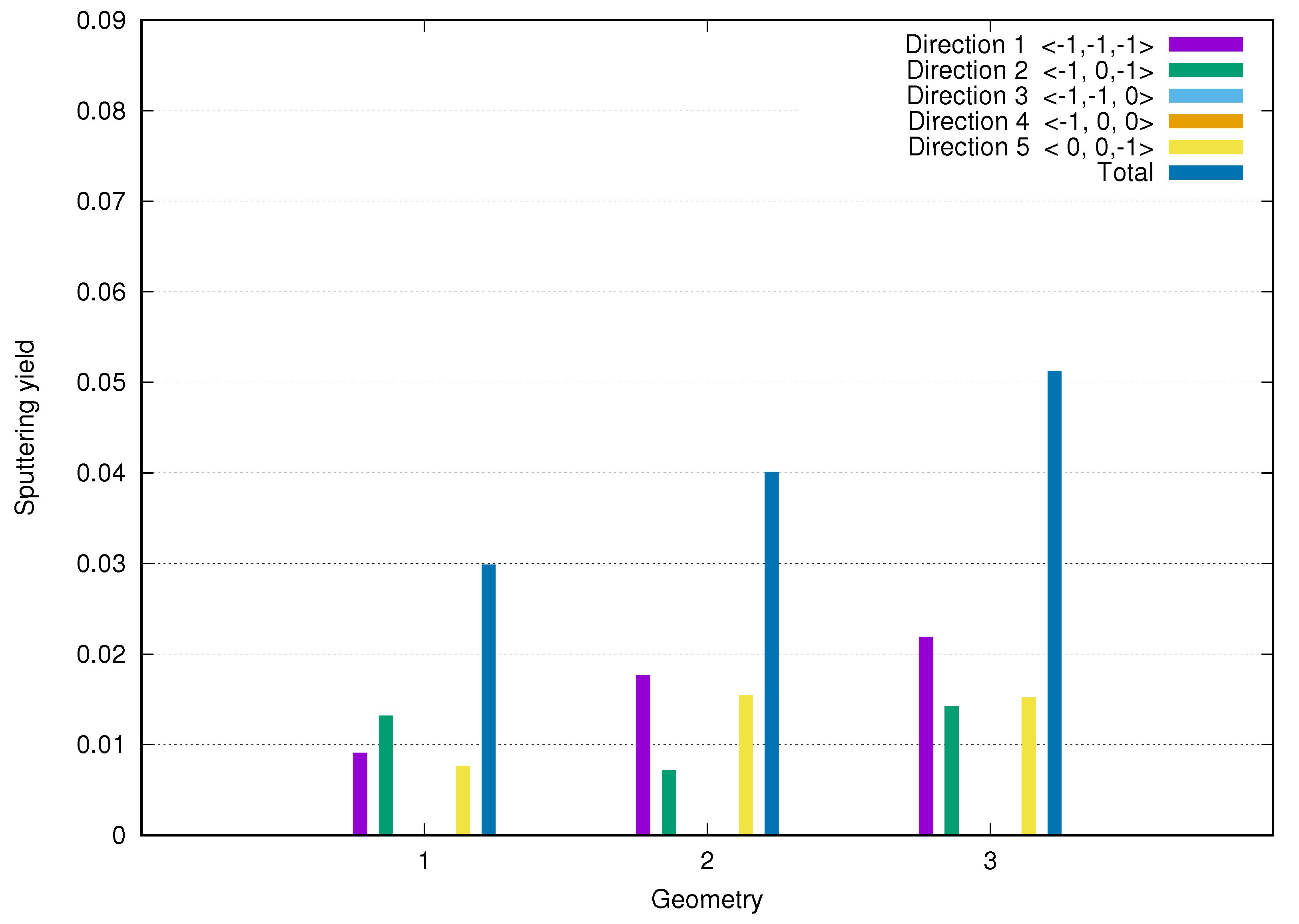
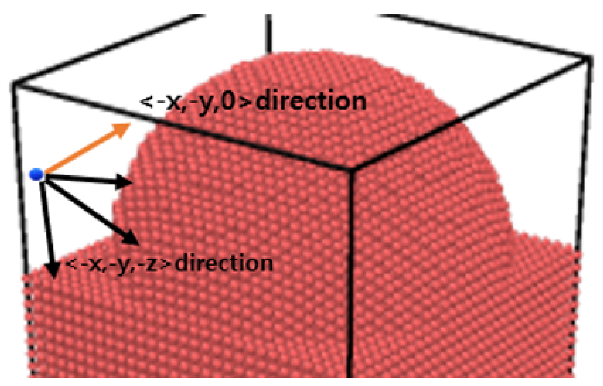
We expected that the energy of the incident particles, the roughness of the divertor surface, and the direction of the incident particles would affect the results. To examine the effect of the incident direction used, we analyzed the effects of five directions. The incident directions of He ions are listed as:
Incident DirectionVector
Direction 1< 1 , 1 , 1 >
Direction 2< 1 , 0, 1 >
Direction 3< 1 , 1 , 0>
Direction 4< 1 , 0, 0>
Direction 5<0, 0, 1 >
For the analysis of the results, we defined the sputtering yield of tungsten atoms released by irradiation as the primary sputtering yield. Additionally, the sputtering yield when re-deposition is taken into account in the primary sputtering yield was called the net sputtering yield.

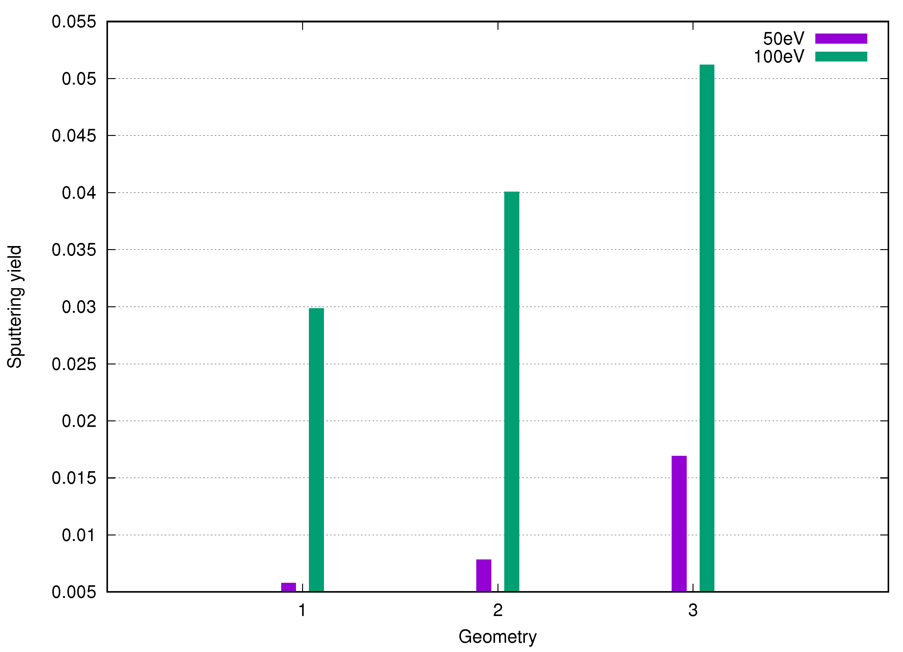
3. Results and Discussion

In our studies, the net sputtering yield defined the number of the net sputtered tungsten atoms per number of impacting helium atoms. Figure 3 shows the evolution of the net sputtering yield over time for the case of geometry 3. The primary sputtering yield tends to decrease over time since the He ions irradiate every 0.5 ps in these simulations. As time goes on, the net sputtering yield is changed drastically as shown in Figure 3. Therefore, choosing a representative value of the net sputtering yield under given conditions is not straightforward. The maximum net sputtering yield value has a large bias because of the outliers. Thus, the maximum net sputtering yield value is not appropriate as the representative value. In order to compare the net sputtering yields, the net sputtering yields were sorted in ascending order. In this study, the lower 5% of the sorted values were arbitrarily selected and analyzed.
Figure 4 shows the net sputtering yield in each geometry. In these simulations, the locations in which the He ions are incident are the same. In the cases of direction 3 and direction 4, the primary sputtering yield is close to zero, since directions 3 and 4 have a zero value on the z component of the vector. This is because when the incident particles had a zero value on the z component of the vector, the He ions collided with the W atoms slightly to geometry 1. Additionally, some incident particles were passed without collision in the cases of geometry 2 and geometry 3. The incident particles having a zero value on the z component of the vector meant that the progress paths of the incident particles were parallel with the x y plane. Therefore, primary sputtering does not occur when the incident He ions do not progress to the curved surface.
On the other hand, directions 1, 2, and 5 have a negative value on the z component of the vector. As shown in Figure 5 if the incident direction has a negative value on the z component of the vector, the incident particles must collide with the target atoms. To make the simulations more realistic, we assembled the results accrued in each direction. As shown in Figure 4, the assembled results show that the net sputtering yield increased as the COD increased, since the number of W atoms on the surface increased. Figure 6 shows the schematic illustration of the change in the number of primary sputtered atoms as the COD increased. Where the surface was flat, the W atoms bonded with the four other W atoms. However, at the dome surface, the number of atomic bondings of the W atoms decreased as the COD increased. Reducing the number of atomic bondings of W atoms means that the W atoms sputter more easily than they do before reducing the number of atomic bondings of W atoms. In other words, the primary sputtering yield increased as the COD increased.
Figure 7 shows the plots of the net sputtering yield when the incident He ions energies are 50 eV and 100 eV. For convenience of explanation, we defined the energy at the time of collision with the surface particles of the target as the remaining energy. When the incident particle collides with the target atoms, primary sputtering occurs if the remaining energy of the incident particle is greater than the bonding energy of the W atoms. The remaining energy increases as the energy of the incident He ion increases. Therefore, the simulation results at 50 eV and 100 eV are shown as shown in Figure 7.
Experimental studies [15,19,20] show that the net sputtering yield decreased as the COD increased. In these experimental studies [15,19,20], the decrease in net sputtering yield according to the COD increase was explained as the increase in the re-deposition rate. For convenience, COD is expressed as λ , primary sputtering yield as α , and re-deposition yield as β . The net sputtering yield γ is given by the difference between α and β , as shown in Equation (3):
γ ( λ ) = α ( λ ) β ( λ )
As explained by former studies [15,19,20] and Figure 6, we have:
α ( λ ) λ = α λ > 0
β ( λ ) λ = β λ > 0
Therefore, the change in the net sputtering yield according to the lambda change is given by Equation (6):
d γ ( λ ) d λ = γ λ = α λ β λ
It can be reasonably inferred that both α λ and β λ are positive numbers from the results of the studies so far; however, a reasonable explanation for the magnitude relationship between the two quantities has not yet been found. In our simulations, the re-deposition yields were relatively small; thus, it was difficult to compare the magnitude of α λ and β λ with a high reliability. In previous studies [15,19,20], the net sputtering yield according to the λ change was explained through the explanation that β λ is positive and, therefore, γ λ is also positive. However, this is an incomplete explanation, as it does not take into account α λ . Of course, if ones examines the actual atomic scale, it is possible to say that α λ 0 is negligible. In this study, the effect was evaluated as not being marginal. Of course, since this molecular dynamics methodology or potential always calculates approximate values, this discrepancy exists due to the limitation of the accuracy of the simulation method used. However, the results of this study also raise the need to re-verify whether factors other than particle curvature are well-controlled when evaluating tungsten sputtering yield.

4. Conclusions

We conducted a tungsten divertor sputtering simulation using molecular dynamics. Both primary sputtering yield and re-deposition are affected by the curvature of the surface atoms, and former studies have focused on the latter. However, since the number of bonds of surface tungsten atoms varies depending on the curvature, the primary sputtering yield will also increase with the curvature. Thus, we find that the net sputtering yield does increase because of the increase in the primary sputtering yield in our study. The effect of curvature on primary sputtering yield changes has not been discussed comprehensively in existing experimental studies. Therefore, we suggest that an experimental evaluation of the particle curvature effect on the primary sputtering yield of W atoms is needed.

Author Contributions

Conceptualization, K.C.; methodology, J.K. and H.K.; software, J.K. and H.K.; validation, K.C. and H.K.; formal analysis, H.K.; investigation, J.K. and H.K.; resources, J.K. and H.K.; data curation, H.K.; writing—original draft preparation, H.K.; writing—review and editing, K.C.; visualization, H.K.; supervision, K.C.; project administration, K.C.; funding acquisition, K.C. All authors have read and agreed to the published version of the manuscript.

Funding

This study was supported by a National Research Foundation of Korea (NRF) grant funded by the Korean government (MSIT) (NRF-2019M1A7A1A02085179). This work was also supported by the “Human Resources Program in Energy Technology” of the Korea Institute of Energy Technology Evaluation and Planning (KETEP), granted financial resources from the Ministry of Trade, Industry Energy, Republic of Korea (No. 20214000000070).

Data Availability Statement

Not applicable.

Conflicts of Interest

The authors declare no conflict of interest.

References

  1. Kammash, T.; Ragheb, M.M.; Higgins, T.J. Fusion reactor physics, principles and technology. IEEE Trans. Nucl. Sci. 1976, 23, 1304–1306. [Google Scholar] [CrossRef]
  2. Miyamoto, K. Plasma Physics for Nuclear Fusion; MIT Press: Cambridge, MA, USA, 1980. [Google Scholar]
  3. Guo, H.; Matthews, G.; Coffey, I.; Erents, S.; Groth, M.; Harbour, P.; Von Hellermann, M.; Hillis, D.; Hogan, J.; Horton, L.; et al. Effects of divertor geometry and chemical sputtering on impurity behaviour and plasma performance in JET. Nucl. Fusion 2000, 40, 379. [Google Scholar] [CrossRef] [Green Version]
  4. Kwon, T.H.; Park, S.; Ha, J.M.; Youn, Y.S. Study on sputtering yield of tungsten with different particle sizes: Surface roughness dependence. Nucl. Eng. Technol. 2021, 53, 1939–1941. [Google Scholar] [CrossRef]
  5. Sigmund, P. Sputtering by ion bombardment theoretical concepts. In Sputtering by Particle Bombardment I; Springer: Berlin/Heidelberg, Germany, 1981; pp. 9–71. [Google Scholar]
  6. Roth, J. Sputtering of limiter and divertor materials. J. Nucl. Mater. 1990, 176, 132–141. [Google Scholar] [CrossRef]
  7. Vörtler, K.; Björkas, C.; Nordlund, K. The effect of plasma impurities on the sputtering of tungsten carbide. J. Phys. Condens. Matter 2011, 23, 085002. [Google Scholar] [CrossRef] [PubMed]
  8. Hirooka, Y.; Bourham, M.; Brooks, J.; Causey, R.; Chevalier, G.; Conn, R.; Eddy, W.; Gilligan, J.; Khandagle, M.; Ra, Y. Evaluation of tungsten as a plasma-facing material for steady state magnetic fusion devices. J. Nucl. Mater. 1992, 196, 149–158. [Google Scholar] [CrossRef]
  9. Wielunska, B.; Mayer, M.; Schwarz-Selinger, T.; Sand, A.; Jacob, W. Deuterium retention in tungsten irradiated by different ions. Nucl. Fusion 2020, 60, 096002. [Google Scholar] [CrossRef]
  10. Rieth, M.; Doerner, R.; Hasegawa, A.; Ueda, Y.; Wirtz, M. Behavior of tungsten under irradiation and plasma interaction. J. Nucl. Mater. 2019, 519, 334–368. [Google Scholar] [CrossRef]
  11. Xie, H.; Ding, R.; Kirschner, A.; Chen, J.; Ding, F.; Mao, H.; Feng, W.; Borodin, D.; Wang, L. ERO modelling of tungsten erosion and re-deposition in EAST L mode discharges. Phys. Plasmas 2017, 24, 092512. [Google Scholar] [CrossRef]
  12. Nishijima, D.; Baldwin, M.; Doerner, R.; Yu, J. Sputtering properties of tungsten ‘fuzzy’surfaces. J. Nucl. Mater. 2011, 415, S96–S99. [Google Scholar] [CrossRef]
  13. Neu, R.; Dux, R.; Kallenbach, A.; Pütterich, T.; Balden, M.; Fuchs, J.; Herrmann, A.; Maggi, C.; O’Mullane, M.; Pugno, R.; et al. Tungsten: An option for divertor and main chamber plasma facing components in future fusion devices. Nucl. Fusion 2005, 45, 209. [Google Scholar] [CrossRef]
  14. Chankin, A.; Coster, D.; Dux, R. Monte Carlo simulations of tungsten redeposition at the divertor target. Plasma Phys. Control. Fusion 2014, 56, 025003. [Google Scholar] [CrossRef]
  15. Nakamura, H.; Saito, S.; Ito, A.M.; Takayama, A. Tungsten-Surface-Structure Dependence of Sputtering Yield for a Noble Gas. Plasma Fusion Res. 2016, 11, 2401080. [Google Scholar] [CrossRef] [Green Version]
  16. Van Rooij, G.; Coenen, J.; Aho-Mantila, L.; Brezinsek, S.; Clever, M.; Dux, R.; Groth, M.; Krieger, K.; Marsen, S.; Matthews, G.; et al. Tungsten divertor erosion in all metal devices: Lessons from the ITER like wall of JET. J. Nucl. Mater. 2013, 438, S42–S47. [Google Scholar] [CrossRef] [Green Version]
  17. Krieger, K.; Maier, H.; Neu, R.; Team, A.U. Conclusions about the use of tungsten in the divertor of ASDEX Upgrade. J. Nucl. Mater. 1999, 266, 207–216. [Google Scholar] [CrossRef]
  18. Herrmann, A.; Greuner, H.; Jaksic, N.; Böswirth, B.; Reimold, F.; Scarabosio, A.; Vorbrugg, S.; Wischmeier, M. Design and concept validation of the new solid tungsten divertor for ASDEX Upgrade. Fusion Eng. Des. 2013, 88, 577–580. [Google Scholar] [CrossRef] [Green Version]
  19. Kreter, A.; Brezinsek, S.; Hirai, T.; Kirschner, A.; Krieger, K.; Mayer, M.; Philipps, V.; Pospieszczyk, A.; Samm, U.; Schmitz, O.; et al. Effect of surface roughness and substrate material on carbon erosion and deposition in the TEXTOR tokamak. Plasma Phys. Control. Fusion 2008, 50, 095008. [Google Scholar] [CrossRef] [Green Version]
  20. Li, Y.; Yang, Y.; Short, M.P.; Ding, Z.; Zeng, Z.; Li, J. Ion radiation albedo effect: Influence of surface roughness on ion implantation and sputtering of materials. Nucl. Fusion 2016, 57, 016038. [Google Scholar] [CrossRef] [Green Version]
  21. Beck, D. A new interatomic potential function for helium. Mol. Phys. 1968, 14, 311–315. [Google Scholar] [CrossRef]
  22. Ackland, G.J.; Thetford, R. An improved N-body semi-empirical model for body-centred cubic transition metals. Philos. Mag. A 1987, 56, 15–30. [Google Scholar] [CrossRef]
  23. Ziegler, J.F.; Biersack, J.P. The stopping and range of ions in matter. In Treatise on Heavy-Ion Science; Springer: Berlin/Heidelberg, Germany, 1985; pp. 93–129. [Google Scholar]
  24. Juslin, N.; Wirth, B. Interatomic potentials for simulation of He bubble formation in W. J. Nucl. Mater. 2013, 432, 61–66. [Google Scholar] [CrossRef]
Figure 1. Schematic illustration of primary sputtering and re-deposition processes.
Metals 11 01532 g001
Figure 2. The geometry of the simulation system: each geometry has the same width (9.4956 nm × 9.4956 nm), but the height varies through the curvature of the dome part.
Metals 11 01532 g002
Figure 3. Change of the net sputtering yield over time for the case of geometry 3.
Metals 11 01532 g003
Figure 4. The net sputtering yield for different geometries with He incident directions.
Metals 11 01532 g004
Figure 5. The directions of the progress of incident particles according to the z component. Black arrows have a negative value on the z component of the vector. Orange arrows have a zero value on the z component of the vector. This is because when the z component of the vector has a value of zero, the direction of the orange arrow is parallel in the x y plane.
Metals 11 01532 g005
Figure 6. Changes in the number of bonding of W atoms increased with COD. If the COD increased, then the number of bonding atoms would be decreased.
Metals 11 01532 g006
Figure 7. Net sputtering yield with the change in the energy of incident He ions.
Metals 11 01532 g007
Publisher’s Note: MDPI stays neutral with regard to jurisdictional claims in published maps and institutional affiliations.

