
Defect Healing of MAPbI3 Perovskite Single Crystal Surface by Benzylamine

 ,
, 
Abstract
:1. Introduction
2. Materials and Methods
2.1. Material
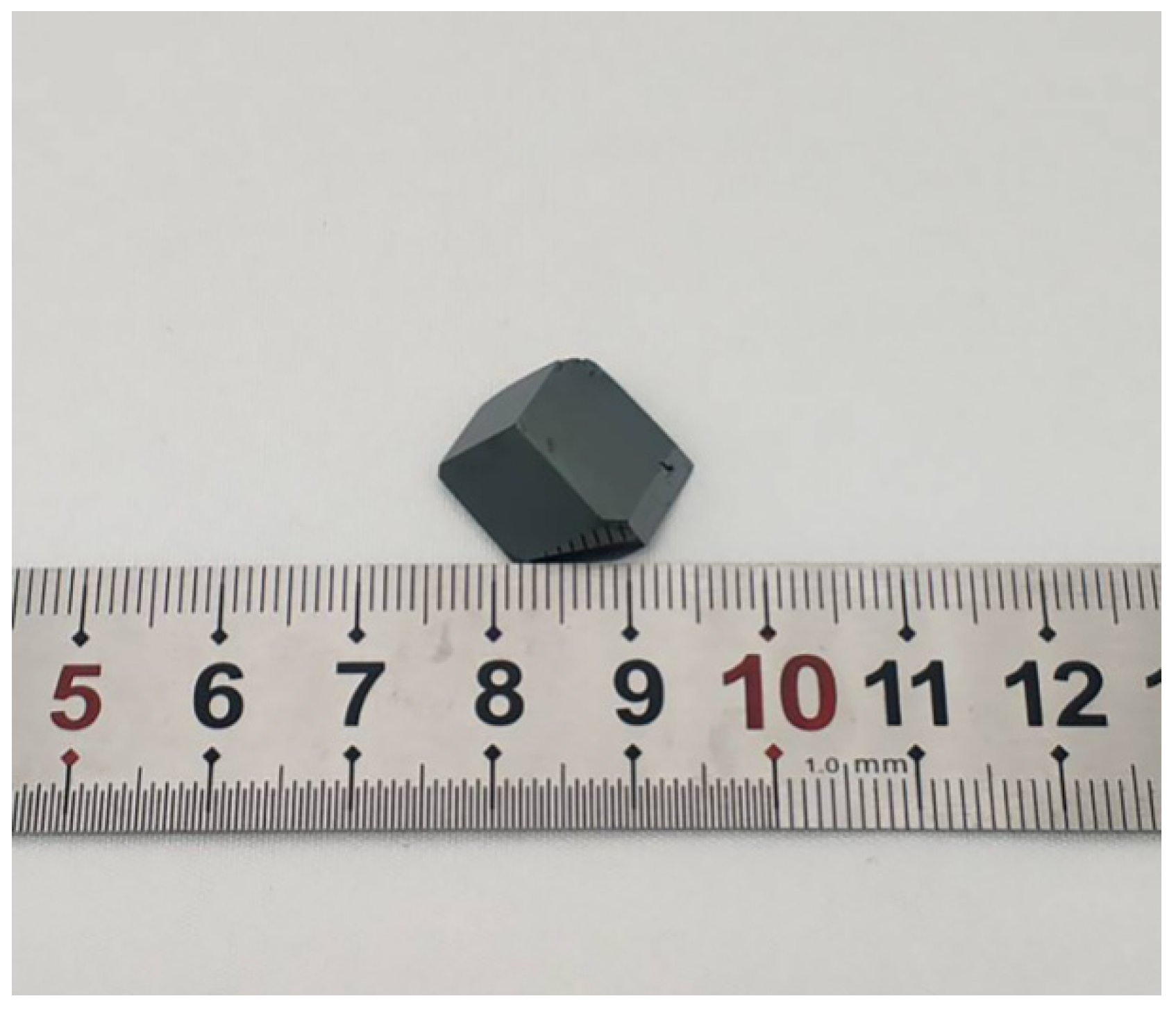
2.2. Growth of MAPbI3 Single Crystal
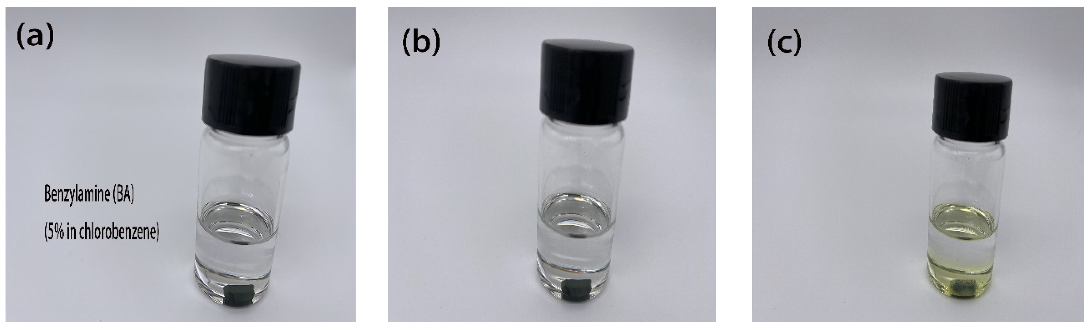
2.3. Process for BA Treatment
2.4. Characterization
3. Results
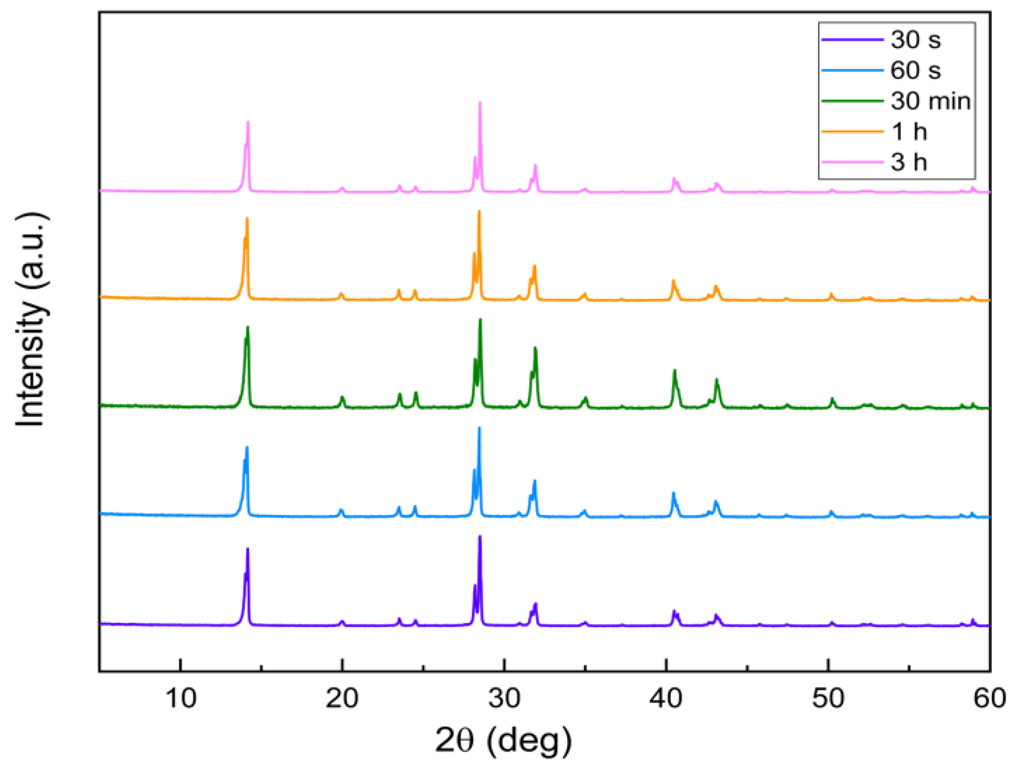
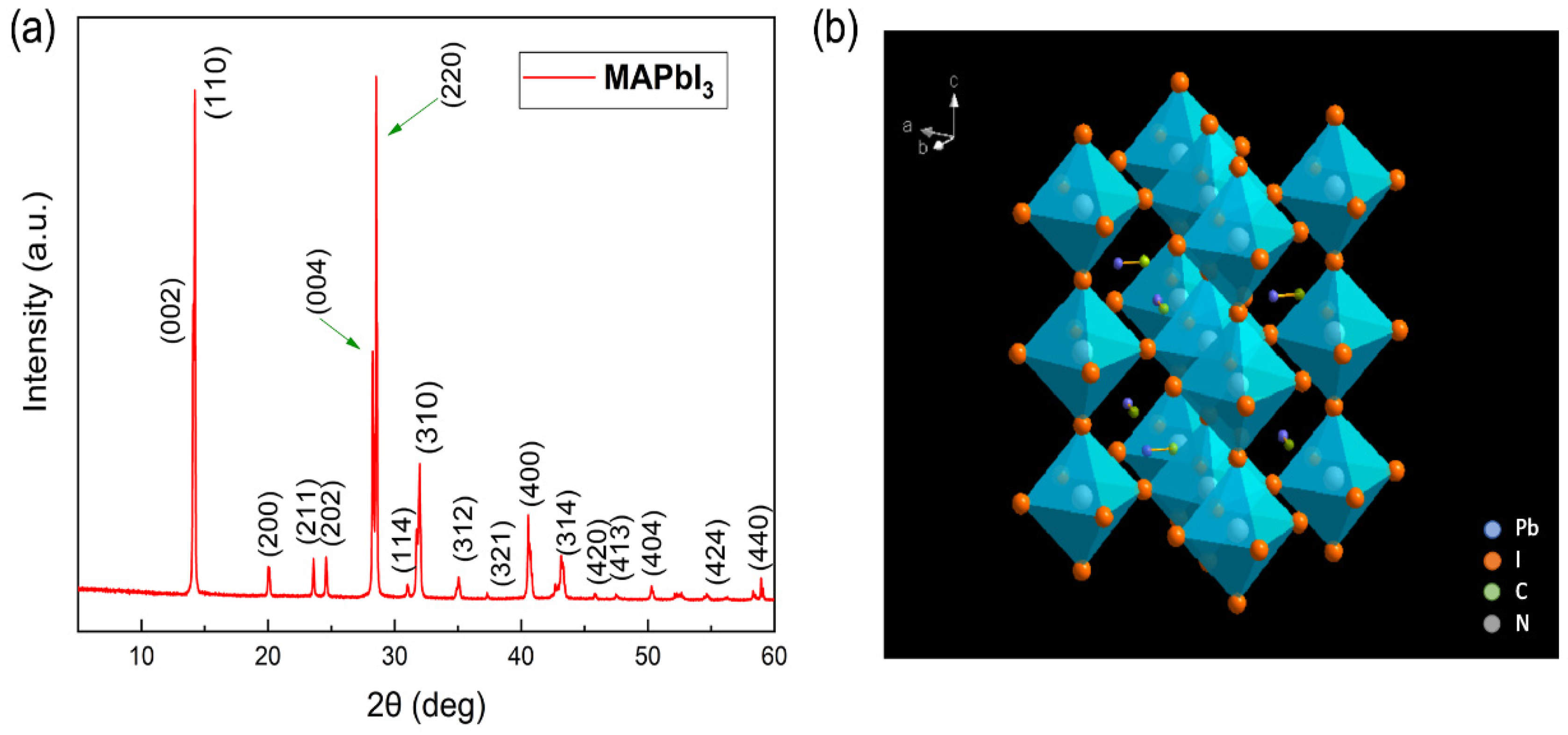
3.1. X-ray Diffraction Characterization of MAPbI3 Crystal
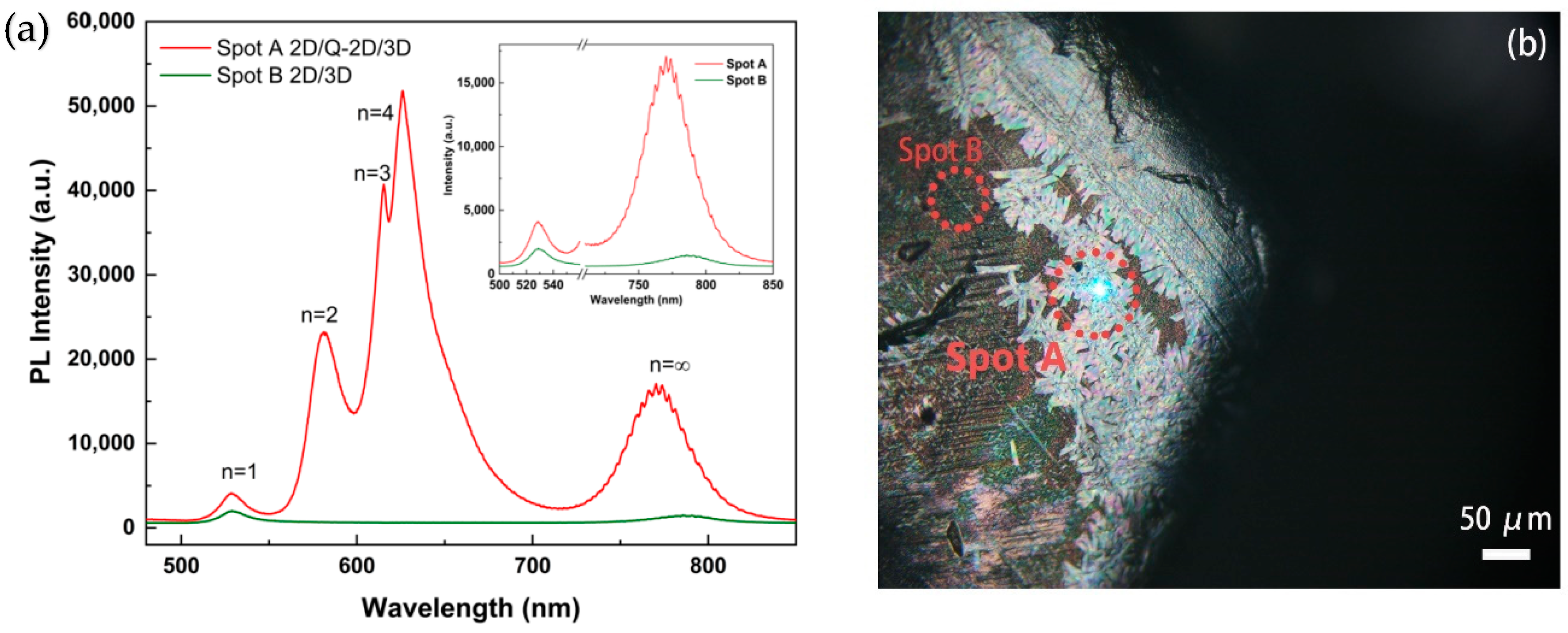
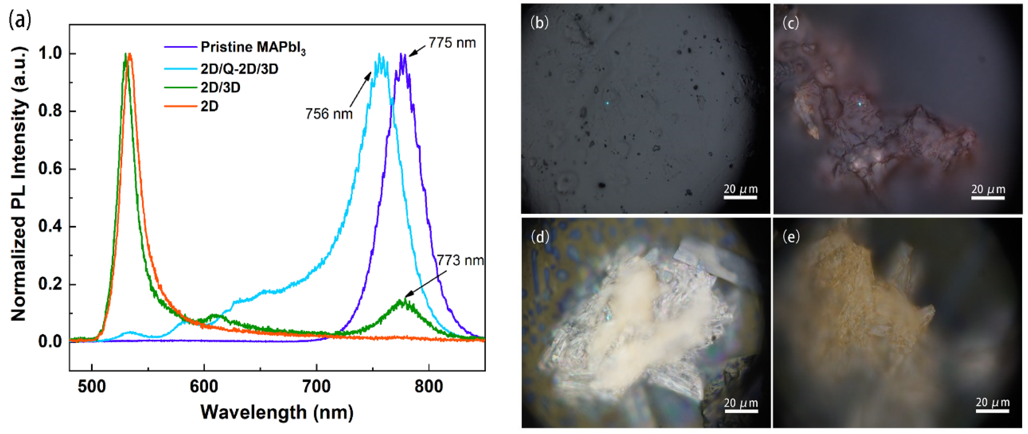
3.2. PL Analysis
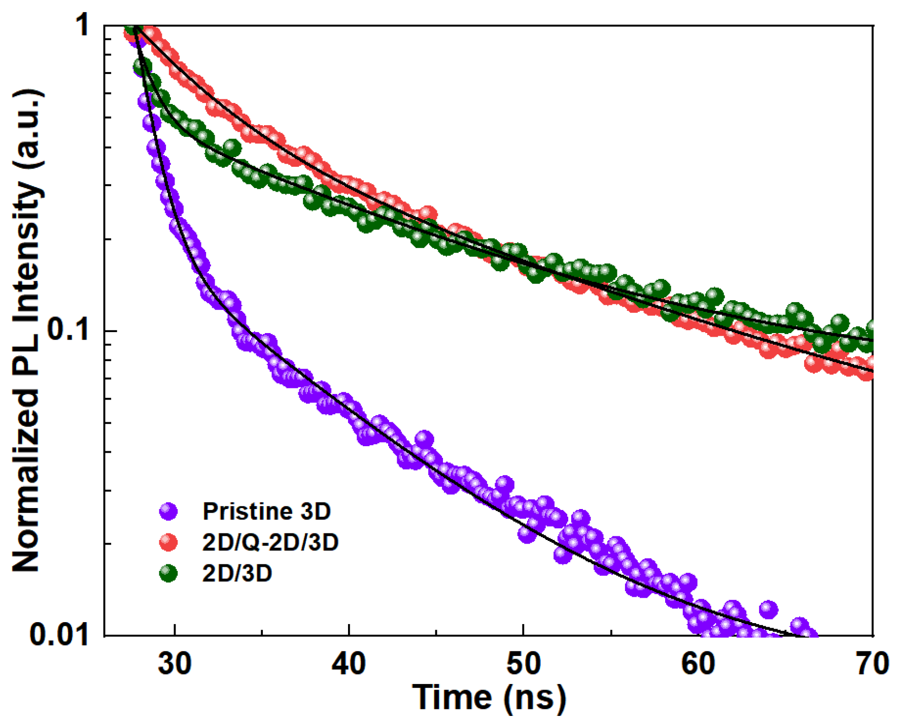
3.3. TRPL Analysis
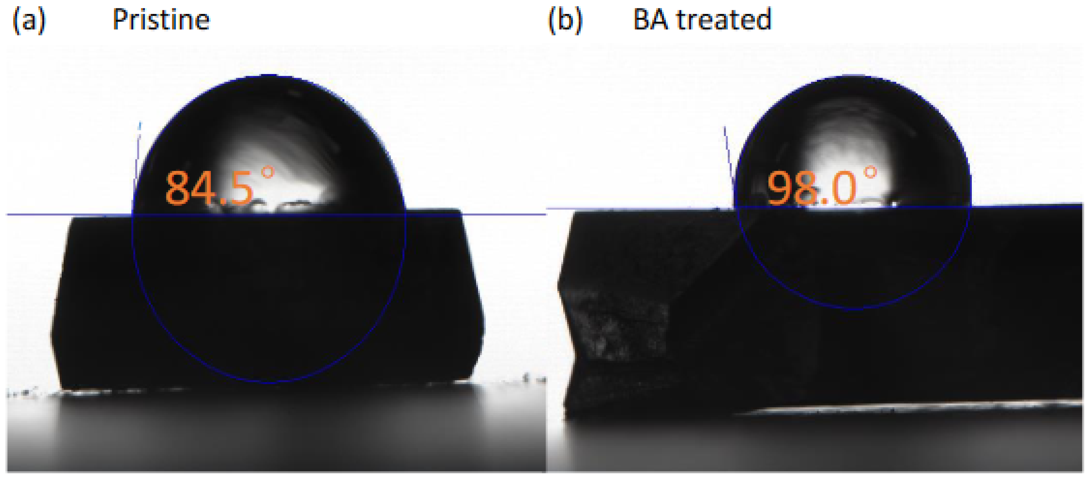
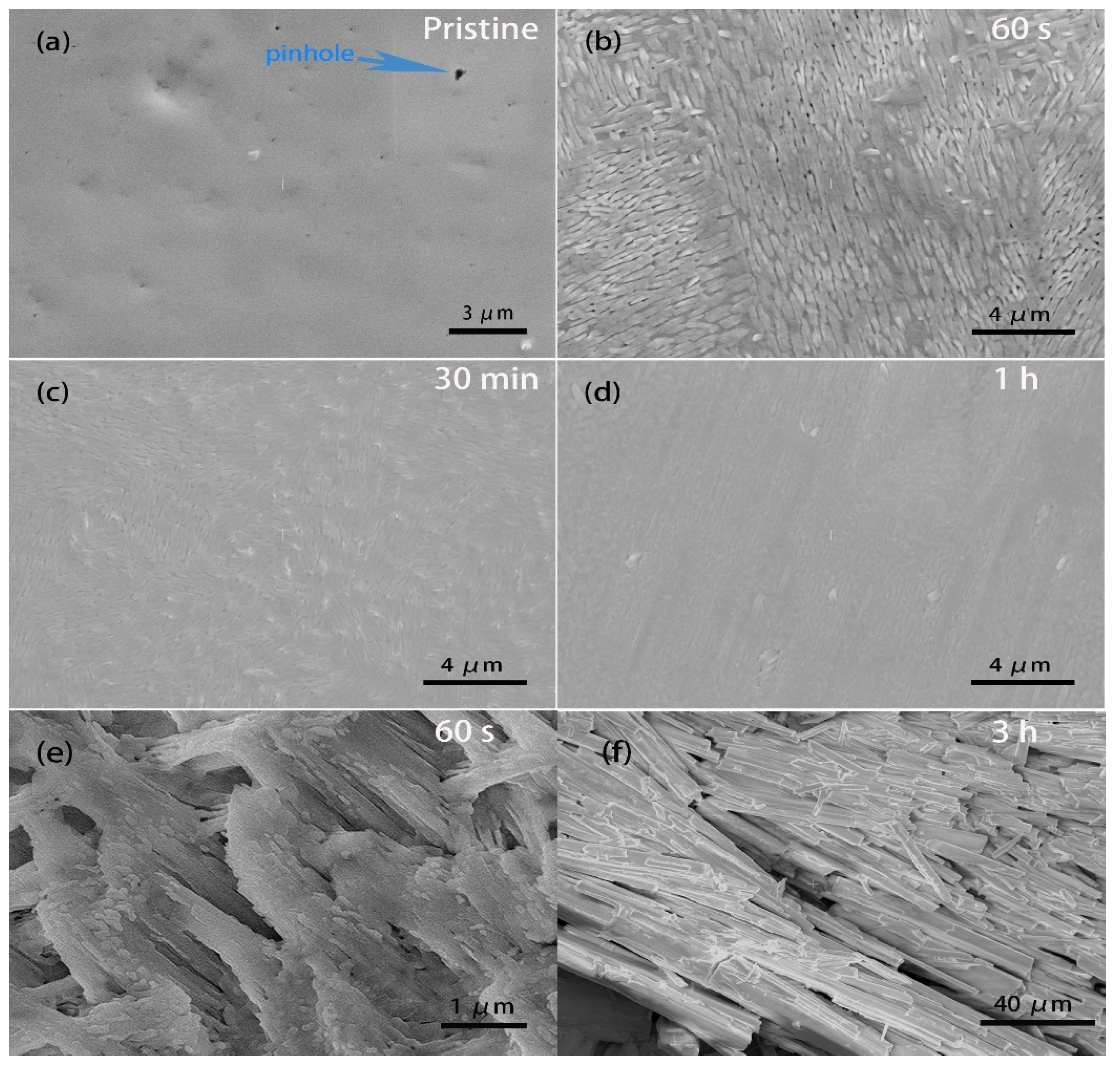
3.4. Surface Morphology and Stability Analysis
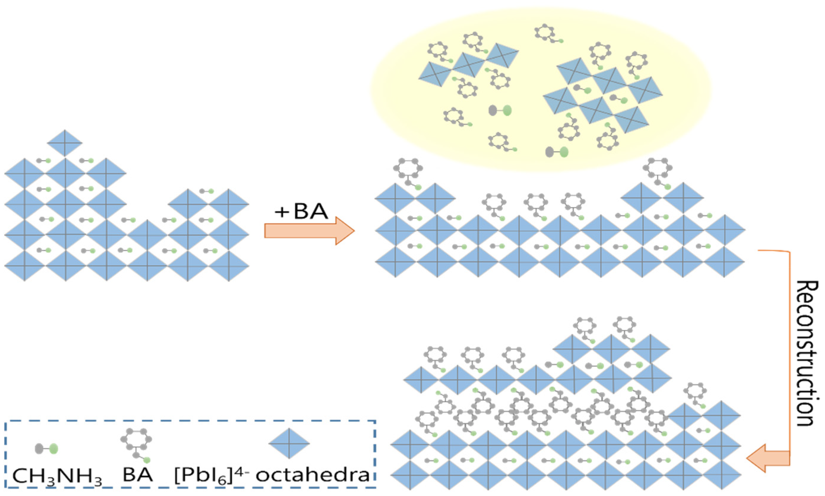
4. Discussion
5. Conclusions
Author Contributions
Funding
Institutional Review Board Statement
Informed Consent Statement
Data Availability Statement
Acknowledgments
Conflicts of Interest
References
- Zhou, H.; Chen, Q.; Li, G.; Luo, S.; Song, T.-B.; Duan, H.-S.; Hong, Z.; You, J.; Liu, Y.; Yang, Y. Interface engineering of highly efficient perovskite solar cells. Science 2014, 345, 542–546. [Google Scholar] [CrossRef] [PubMed]
- Bouich, A.; Mari-Guaita, J.; Bouich, A.; Pradas, I.G.; Mari, B. Towards manufacture stable lead perovskite APbI3 (A = Cs, MA, FA) based solar cells with low-cost techniques. Eng. Proc. 2021, 12, 81. [Google Scholar]
- Marí-Guaita, J.; Bouich, A.; Marí, B. Shedding Light on Phase Stability and Surface Engineering of Formamidinium Lead Iodide (FaPbI3) Thin Films for Solar Cells. Eng. Proc. 2021, 12, 2001. [Google Scholar] [CrossRef]
- Dou, L.; Yang, Y.; You, J.; Hong, Z.; Chang, W.-H.; Li, G. Solution-processed hybrid perovskite photodetectors with high detectivity. Nat. Commun. 2014, 5, 5404. [Google Scholar] [CrossRef] [PubMed]
- Tie, S.; Zhao, W.; Xin, D.; Zhang, M.; Long, J.; Chen, Q.; Zheng, X.; Zhu, J.; Zhang, W. Robust Fabrication of Hybrid Lead-Free Perovskite Pellets for Stable X-ray Detectors with Low Detection Limit. Adv. Mater. 2020, 32, e2001981. [Google Scholar] [CrossRef] [PubMed]
- Tan, Z.K.; Moghaddam, R.S.; Lai, M.L.; Docampo, P.; Higler, R.; Deschler, F.; Price, M.B.; Sadhanala, A.; Pazos-Outon, L.M.; Credgington, D.; et al. Bright light-emitting diodes based on organometal halide perovskite. Nat. Nanotechnol. 2014, 9, 687–692. [Google Scholar] [CrossRef]
- Yuan, M.; Na Quan, L.; Comin, R.; Walters, G.; Sabatini, R.; Voznyy, O.; Hoogland, S.; Zhao, Y.; Beauregard, E.M.; Kanjanaboos, P.; et al. Perovskite energy funnels for efficient light-emitting diodes. Nat. Nanotechnol. 2016, 11, 872–877. [Google Scholar] [CrossRef]
- Zhu, H.; Fu, Y.; Meng, F.; Wu, X.; Gong, Z.; Ding, Q.; Gustafsson, M.V.; Trinh, M.T.; Jin, S.; Zhu, X.-Y. Lead halide perovskite nanowire lasers with low lasing thresholds and high quality factors. Nat. Mater. 2015, 14, 636–642. [Google Scholar] [CrossRef]
- Yoo, E.J.; Lyu, M.; Yun, J.H.; Kang, C.J.; Choi, Y.J.; Wang, L. Resistive Switching Behavior in Organic-Inorganic Hybrid CH3NH3PbI3-xClx Perovskite for Resistive Random Access Memory Devices. Adv. Mater. 2015, 27, 6170–6175. [Google Scholar] [CrossRef]
- Ilin, A.; Forsh, P.A.; Martyshov, M.N.; Kazanskii, A.G.; Forsh, E.A.; Kashkarov, P.K. Humidity Sensing Properties of Organometallic Perovskite CH3NH3PbI3. ChemistrySelect 2020, 5, 6705–6708. [Google Scholar] [CrossRef]
- Ball, J.M.; Petrozza, A. Defects in perovskite-halides and their effects in solar cells. Nat. Energy 2016, 1, 16149. [Google Scholar] [CrossRef]
- Liu, Y.C.; Zhang, Y.X.; Zhu, X.J.; Feng, J.S.; Spanopoulos, I.; Ke, W.J.; He, Y.H.; Ren, X.D.; Yang, Z.; Xiao, F.W.; et al. Triple-Cation and Mixed-Halide Perovskite Single Crystal for High-Performance X-ray Imaging. Adv. Mater. 2021, 33, 2006010. [Google Scholar] [CrossRef] [PubMed]
- Chen, Z.; Turedi, B.; Alsalloum, A.Y.; Yang, C.; Zheng, X.; Gereige, I.; AlSaggaf, A.; Mohammed, O.F.; Bakr, O.M. Single-Crystal MAPbI3 Perovskite Solar Cells Exceeding 21% Power Conversion Efficiency. ACS Energy Lett. 2019, 4, 1258–1259. [Google Scholar] [CrossRef] [Green Version]
- Bi, Y.; Hutter, E.M.; Fang, Y.J.; Dong, Q.F.; Huang, J.S.; Savenije, T.J. Charge Carrier Lifetimes Exceeding 15 mu s in Methylammonium Lead Iodide Single Crystals. J. Phys. Chem. Lett. 2016, 7, 923–928. [Google Scholar] [CrossRef] [PubMed]
- Murali, B.; Yengel, E.; Yang, C.; Peng, W.; Alarousu, E.; Bakr, O.M.; Mohammed, O.F. The Surface of Hybrid Perovskite Crystals: A Boon or Bane. ACS Energy Lett. 2017, 2, 846–856. [Google Scholar] [CrossRef]
- Naghadeh, S.B.; Luo, B.; Abdelmageed, G.; Pu, Y.-C.; Zhang, C.; Zhang, J.Z. Photophysical Properties and Improved Stability of Organic–Inorganic Perovskite by Surface Passivation. J. Phys. Chem. C 2018, 122, 15799–15818. [Google Scholar] [CrossRef]
- Lin, Y.; Bai, Y.; Fang, Y.; Chen, Z.; Yang, S.; Zheng, X.; Tang, S.; Liu, Y.; Zhao, J.; Huang, J. Enhanced Thermal Stability in Perovskite Solar Cells by Assembling 2D/3D Stacking Structures. J. Phys. Chem. Lett. 2018, 9, 654–658. [Google Scholar] [CrossRef]
- Wang, F.; Geng, W.; Zhou, Y.; Fang, H.-H.; Tong, C.-J.; Loi, M.A.; Liu, L.-M.; Zhao, N. Phenylalkylamine Passivation of Organolead Halide Perovskites Enabling High-Efficiency and Air-Stable Photovoltaic Cells. Adv. Mater. 2016, 28, 9986–9992. [Google Scholar] [CrossRef]
- Li, J.; Bu, T.; Lin, Z.; Mo, Y.; Chai, N.; Gao, X.; Ji, M.; Zhang, X.-L.; Cheng, Y.-B.; Huang, F. Efficient and stable perovskite solar cells via surface passivation of an ultrathin hydrophobic organic molecular layer. Chem. Eng. J. 2020, 405, 126712. [Google Scholar] [CrossRef]
- Liu, L.; Xu, K.; Allen, A.L.; Li, X.; Xia, H.; Peng, L.; Zhang, J.Z. Enhancing the Photoluminescence and Stability of Methylammonium Lead Halide Perovskite Nanocrystals with Phenylalanine. J. Phys. Chem. C 2021, 125, 2793–2801. [Google Scholar] [CrossRef]
- Chen, L.; Wang, H.; Zhang, W.; Li, F.; Wang, Z.; Wang, X.; Shao, Y.; Shao, J. Surface Passivation of MAPbBr3 Perovskite Single Crystals to Suppress Ion Migration and Enhance Photoelectronic Performance. ACS Appl. Mater. Interfaces 2022, 14, 10917–10926. [Google Scholar] [CrossRef] [PubMed]
- Wang, W.; Cai, M.; Wu, G.; Zhu, L.; Liu, X.; Lv, H.; Dai, S. Facet Control of the Lead-Free Methylammonium Bismuth Iodide Perovskite Single Crystals via Ligand-Mediated Strategy. Cryst. Growth Des. 2021, 21, 5840–5847. [Google Scholar] [CrossRef]
- Leblebici, S.Y.; Leppert, L.; Li, Y.; Reyes-Lillo, S.E.; Wickenburg, S.; Wong, E.; Lee, J.; Melli, M.; Ziegler, D.; Angell, D.K.; et al. Facet-dependent photovoltaic efficiency variations in single grains of hybrid halide perovskite. Nat. Energy 2016, 1, 16093. [Google Scholar] [CrossRef]
- Lv, Q.R.; He, W.H.; Lian, Z.P.; Ding, J.; Li, Q.; Yan, Q.F. Anisotropic moisture erosion of CH3NH3PbI3 single crystals. Crystengcomm 2017, 19, 901–904. [Google Scholar] [CrossRef]
- Kim, D.; Yun, J.-H.; Lyu, M.; Kim, J.; Lim, S.; Yun, J.S.; Wang, L.; Seidel, J. Probing Facet-Dependent Surface Defects in MAPbI3 Perovskite Single Crystals. J. Phys. Chem. C 2019, 123, 14144–14151. [Google Scholar] [CrossRef]
- Saidaminov, M.; Abdelhady, A.; Murali, B.; Alarousu, E.; Burlakov, V.M.; Peng, W.; Dursun, I.; Wang, L.; He, Y.; Maculan, G.; et al. High-quality bulk hybrid perovskite single crystals within minutes by inverse temperature crystallization. Nat. Commun. 2015, 6, 7586. [Google Scholar] [CrossRef] [Green Version]
- Liu, Y.C.; Yang, Z.; Cui, D.; Ren, X.D.; Sun, J.K.; Liu, X.J.; Zhang, J.R.; Wei, Q.B.; Fan, H.B.; Yu, F.Y.; et al. Two-Inch-Sized Perovskite CH3NH3PbX3 (X = Cl, Br, I) Crystals: Growth and Characterization. Adv. Mater. 2015, 27, 5176–5183. [Google Scholar] [CrossRef]
- Dong, Q.F.; Fang, Y.J.; Shao, Y.C.; Mulligan, P.; Qiu, J.; Cao, L.; Huang, J.S. Electron-hole diffusion lengths >175 μm in solution-grown CH3NH3PbI3 single crystals. Science 2015, 347, 967–970. [Google Scholar] [CrossRef] [Green Version]
- Baikie, T.; Fang, Y.; Kadro, J.M.; Schreyer, M.; Wei, F.; Mhaisalkar, S.G.; Graetzel, M.; White, T.J. Synthesis and crystal chemistry of the hybrid perovskite (CH3NH3)PbI3 for solid-state sensitised solar cell applications. J. Mater. Chem. A 2013, 1, 5628–5641. [Google Scholar] [CrossRef]
- Shi, D.; Adinolfi, V.; Comin, R.; Yuan, M.; Alarousu, E.; Buin, A.; Chen, Y.; Hoogland, S.; Rothenberger, A.; Katsiev, K.; et al. Low trap-state density and long carrier diffusion in organolead trihalide perovskite single crystals. Science 2015, 347, 519–522. [Google Scholar] [CrossRef] [Green Version]
- Whitfield, P.S.; Herron, N.; Guise, W.E.; Page, K.; Cheng, Y.Q.; Milas, I.; Crawford, M.K. Structures, Phase Transitions and Tricritical Behavior of the Hybrid Perovskite Methyl Ammonium Lead Iodide. Sci. Rep. 2016, 6, 35685. [Google Scholar] [CrossRef] [PubMed] [Green Version]
- Dang, Y.Y.; Liu, Y.; Sun, Y.X.; Yuan, D.S.; Liu, X.L.; Lu, W.Q.; Liu, G.F.; Xia, H.B.; Tao, X.T. Bulk crystal growth of hybrid perovskite material CH3NH3PbI3. Crystengcomm 2015, 17, 665–670. [Google Scholar] [CrossRef]
- Wu, X.; Trinh, M.T.; Niesner, D.; Zhu, H.; Norman, Z.; Owen, J.S.; Yaffe, O.; Kudisch, B.J.; Zhu, X.-Y. Trap States in Lead Iodide Perovskites. J. Am. Chem. Soc. 2015, 137, 2089–2096. [Google Scholar] [CrossRef] [PubMed]
- Yang, X.L.; Zhang, X.W.; Deng, J.X.; Chu, Z.M.; Jiang, Q.; Meng, J.H.; Wang, P.Y.; Zhang, L.Q.; Yin, Z.G.; You, J.B. Efficient green light-emitting diodes based on quasi-two-dimensional composition and phase engineered perovskite with surface passivation. Nat. Commun. 2018, 9, 570. [Google Scholar] [CrossRef] [PubMed]
- Mao, L.; Stoumpos, C.C.; Kanatzidis, M.G. Two-Dimensional Hybrid Halide Perovskites: Principles and Promises. J. Am. Chem. Soc. 2018, 141, 1171–1190. [Google Scholar] [CrossRef]
- Sun, M.; Zhang, F.; Liu, H.; Li, X.; Xiao, Y.; Wang, S. Tuning the crystal growth of perovskite thin-films by adding the 2-pyridylthiourea additive for highly efficient and stable solar cells prepared in ambient air. J. Mater. Chem. A 2017, 5, 13448–13456. [Google Scholar] [CrossRef]
- Liu, J.; Leng, J.; Wu, K.; Zhang, J.; Jin, S. Observation of Internal Photoinduced Electron and Hole Separation in Hybrid Two-Dimentional Perovskite Films. J. Am. Chem. Soc. 2017, 139, 1432–1435. [Google Scholar] [CrossRef]
- Lu, Y.-B.; Guan, C.; Sun, H.; Cong, W.-Y.; Yang, H.; Zhang, P. Investigation on Enhanced Moisture Resistance of Two-Dimensional Layered Hybrid Organic–Inorganic Perovskites (C4H9NH3)2PbI4. J. Phys. Chem. C 2018, 122, 11862–11869. [Google Scholar] [CrossRef]
- Zhumekenov, A.A.; Saidaminov, M.I.; Haque, A.; Alarousu, E.; Sarmah, S.P.; Murali, B.; Dursun, I.; Miao, X.-H.; Abdelhady, A.; Wu, T.; et al. Formamidinium Lead Halide Perovskite Crystals with Unprecedented Long Carrier Dynamics and Diffusion Length. ACS Energy Lett. 2016, 1, 32–37. [Google Scholar] [CrossRef]
- Soe, C.M.M.; Nie, W.; Stoumpos, C.; Tsai, H.; Blancon, J.-C.; Liu, F.; Even, J.; Marks, T.J.; Mohite, A.D.; Kanatzidis, M.G. Understanding Film Formation Morphology and Orientation in High Member 2D Ruddlesden–Popper Perovskites for High-Efficiency Solar Cells. Adv. Energy Mater. 2017, 8, 1700979. [Google Scholar] [CrossRef]
- Tavakoli, M.M.; Zakeeruddin, S.M.; Grätzel, M.; Fan, Z. Large-Grain Tin-Rich Perovskite Films for Efficient Solar Cells via Metal Alloying Technique. Adv. Mater. 2018, 30, 1705998. [Google Scholar] [CrossRef] [PubMed] [Green Version]
- Zhou, Z.M.; Wang, Z.W.; Zhou, Y.Y.; Pang, S.P.; Wang, D.; Xu, H.X.; Liu, Z.H.; Padture, N.P.; Cui, G.L. Methylamine-Gas-Induced Defect-Healing Behavior of CH3NH3PbI3 Thin Films for Perovskite Solar Cells. Angew. Chem. Int. Ed. 2015, 54, 9705–9709. [Google Scholar] [CrossRef] [PubMed]
- Warren, R.F.; Liang, W.Y. Raman spectroscopy of new lead iodide intercalation compounds. J. Phys. Condens. Matter 1993, 5, 6407–6418. [Google Scholar] [CrossRef]
- Bučko, T.; Hafner, J.; Lebègue, S.; Ángyán, J.G. Improved Description of the Structure of Molecular and Layered Crystals: Ab Initio DFT Calculations with van der Waals Corrections. J. Phys. Chem. A 2010, 114, 11814–11824. [Google Scholar] [CrossRef] [PubMed]
- Duim, H.; Fang, H.-H.; Adjokatse, S.; Brink, G.H.T.; Marques, M.A.L.; Kooi, B.J.; Blake, G.R.; Botti, S.; Loi, M.A. Mechanism of surface passivation of methylammonium lead tribromide single crystals by benzylamine. Appl. Phys. Rev. 2019, 6, 031401. [Google Scholar] [CrossRef]
- Grancini, G.; Roldán-Carmona, C.; Zimmermann, I.; Mosconi, E.; Lee, X.; Martineau, D.; Narbey, S.; Oswald, F.; De Angelis, F.; Graetzel, M.; et al. One-Year stable perovskite solar cells by 2D/3D interface engineering. Nat. Commun. 2017, 8, 15684. [Google Scholar] [CrossRef]
- Younas, M.; Gondal, M.A.; Dastageer, M.A. Fabrication of perovskite solar cells using novel 2D/3D-blended perovskite single crystals. Int. J. Energy Res. 2020, 45, 5555–5566. [Google Scholar] [CrossRef]
- Lei, Y.; Chen, Y.; Zhang, R.; Li, Y.; Yan, Q.; Lee, S.; Yu, Y.; Tsai, H.; Choi, W.; Wang, K.; et al. A fabrication process for flexible single-crystal perovskite devices. Nature 2020, 583, 790–795. [Google Scholar] [CrossRef]
- Zhang, X.Y.; Ji, C.M.; Liu, X.T.; Wang, S.S.; Li, L.N.; Peng, Y.; Yao, Y.P.; Hong, M.C.; Luo, J.H. Solution-Grown Large-Sized Single-Crystalline 2D/3D Perovskite Heterostructure for Self-Powered Photodetection. Adv. Opt. Mater. 2020, 8, 2000311. [Google Scholar] [CrossRef]
- Zhou, Y.; Zhao, L.; Ni, Z.; Xu, S.; Zhao, J.; Xiao, X.; Huang, J. Heterojunction structures for reduced noise in large-area and sensitive perovskite X-ray detectors. Sci. Adv. 2021, 7, eabg6716. [Google Scholar] [CrossRef]
- He, Y.; Pan, W.; Guo, C.; Zhang, H.; Wei, H.; Yang, B. 3D/2D Perovskite Single Crystals Heterojunction for Suppressed Ions Migration in Hard X-ray Detection. Adv. Funct. Mater. 2021, 31, 2104880. [Google Scholar] [CrossRef]


| Sample | Pristine MAPbI3 | 2D/Q-2D/3D | 2D/3D |
|---|---|---|---|
| τ1 (ns) | 1.06 | 4.57 | 1.09 |
| τ2 (ns) | 9.03 | 19.92 | 15.42 |
Publisher’s Note: MDPI stays neutral with regard to jurisdictional claims in published maps and institutional affiliations. |
© 2022 by the authors. Licensee MDPI, Basel, Switzerland. This article is an open access article distributed under the terms and conditions of the Creative Commons Attribution (CC BY) license (https://creativecommons.org/licenses/by/4.0/).
Share and Cite
Wang, W.; Cai, M.; Wu, Y.; Ji, K.; Cheng, B.; Liu, X.; Lv, H.; Dai, S. Defect Healing of MAPbI3 Perovskite Single Crystal Surface by Benzylamine. Symmetry 2022, 14, 1099. https://doi.org/10.3390/sym14061099
Wang W, Cai M, Wu Y, Ji K, Cheng B, Liu X, Lv H, Dai S. Defect Healing of MAPbI3 Perovskite Single Crystal Surface by Benzylamine. Symmetry. 2022; 14(6):1099. https://doi.org/10.3390/sym14061099
Chicago/Turabian StyleWang, Wenjun, Molang Cai, Yunzhao Wu, Kangyu Ji, Bin Cheng, Xuepeng Liu, Hui Lv, and Songyuan Dai. 2022. "Defect Healing of MAPbI3 Perovskite Single Crystal Surface by Benzylamine" Symmetry 14, no. 6: 1099. https://doi.org/10.3390/sym14061099
APA StyleWang, W., Cai, M., Wu, Y., Ji, K., Cheng, B., Liu, X., Lv, H., & Dai, S. (2022). Defect Healing of MAPbI3 Perovskite Single Crystal Surface by Benzylamine. Symmetry, 14(6), 1099. https://doi.org/10.3390/sym14061099