Article

Investigation of Heavy-Ion Induced Single-Event Transient in 28 nm Bulk Inverter Chain

College of Computer, National University of Defense Technology, Changsha 410073, China
*
Author to whom correspondence should be addressed.
Symmetry 2020, 12(4), 624; https://doi.org/10.3390/sym12040624
Submission received: 29 March 2020 / Revised: 10 April 2020 / Accepted: 11 April 2020 / Published: 15 April 2020

Abstract

:
The reliability of integrated circuits under advanced process nodes is facing more severe challenges. Single-event transients (SET) are an important cause of soft errors in space applications. The SET caused by heavy ions in the 28 nm bulk silicon inverter chains was studied. A test chip with good symmetry layout design was fabricated based on the 28 nm process, and the chip was struck by using 5 kinds of heavy ions with different linear energy transfer (LET) values on heavy-ion accelerator. The research results show that in advanced technology, smaller sensitive volume makes SET cross-section measured at 28 nm smaller than 65 nm by an order of magnitude, the lower critical charge required to generate SET will increase the reliability threat of low-energy ions to the circuit, and high-energy ions are more likely to cause single-event multiple transient (SEMT), which cannot be ignored in practical circuits. The transients pulse width data can be used as a reference for SET modeling in complex circuits.

1. Introduction

The generation of soft errors caused by radiation-induced single-event transients (SET) is a significant reliability challenge in modern complementary metal-oxide-semiconductor (CMOS) logic, both in space applications and in terrestrial applications [1,2,3]. As process feature sizes continue to shrink, clock frequencies continue to increase, node capacitance and supply voltage decrease, the critical charge of transient pulses is reduced [3,4,5], and waveforms are more easily captured and soft errors are formed. It has been reported that SET are the main cause of soft errors in space applications [6,7], and charge sharing may even affect multiple nodes and cause single-event multiple transients (SEMT) [8,9,10]. These problems are already common in combinatorial logic circuits. The impact of SET has attracted a lot of attention, but its characterization is complicated because the cross section and pulse width must be measured simultaneously [6]. There have been many experimental studies on SET. The results measured at the 0.25, 0.18, and 0.13 μ m process nodes show that the effect of voltage variation on the relationship between the SET pulse width and the cross section cannot be ignored [11]. Experiments with heavy ions on 130 nm and 90 nm chips have shown that the Linear energy transfer (LET) threshold for generating SET becomes lower as process size decreases [12], which can make the soft error problem under advanced process nodes even more severe. Reference [13] compares the results of SET measurements in the 65 nm bulk silicon process with 130 nm and 90 nm. It is found that the propagation induced pulse broadening and parasitic bipolar amplification effect make the trend of SET pulse width more and more complicated. In Reference [14], pulse quenching can also affect SET. At the 65 nm process node, a lot of research has been done on the characterization of SET [3,15,16,17,18], but in more advanced processes, the results of experimental measurements on SET are still few.
In the study of measuring the pulse width, there was originally a method based on oscilloscope to measure current pulses [19], but the defects of this off-chip test method are very obvious. The load resistance and line capacitance of the test system cause large pulse distortion, and the on-chip measurement is believed to be a better solution in most applications, and Narasimham et al. [20] invented a self-triggering technique for measuring SET pulses in 130 nm and 90 nm chips in Reference [12]. In other processes, there are also examples [3,9,13,14] of successful use of this measurement method. On the basis of this method, Huang et al. [8] proposed a structure that can simultaneously measure multiple transient pulses, using eight capture circuits to share a self-trigger structure design, which can measure the SEMT. This improvement has also been widely used by researchers [6,10,18].
In this paper, the heavy-ion induced SET pulse measurement structure proposed in Reference [8] is used and some additional measures are taken. A test chip was fabricated in a 28 nm bulk silicon process using eight inverter chains as a sensitive target circuit. Radiation experiments were carried out on the test chip using a variety of heavy ions (with LET values from 9.0 to 81.35 MeV · cm 2 · mg 1 ), the measured SET pulse width and cross section are analyzed. Our intent is that this test data and the situation discussed may be used for calibration to model single-event transients in complex circuits.

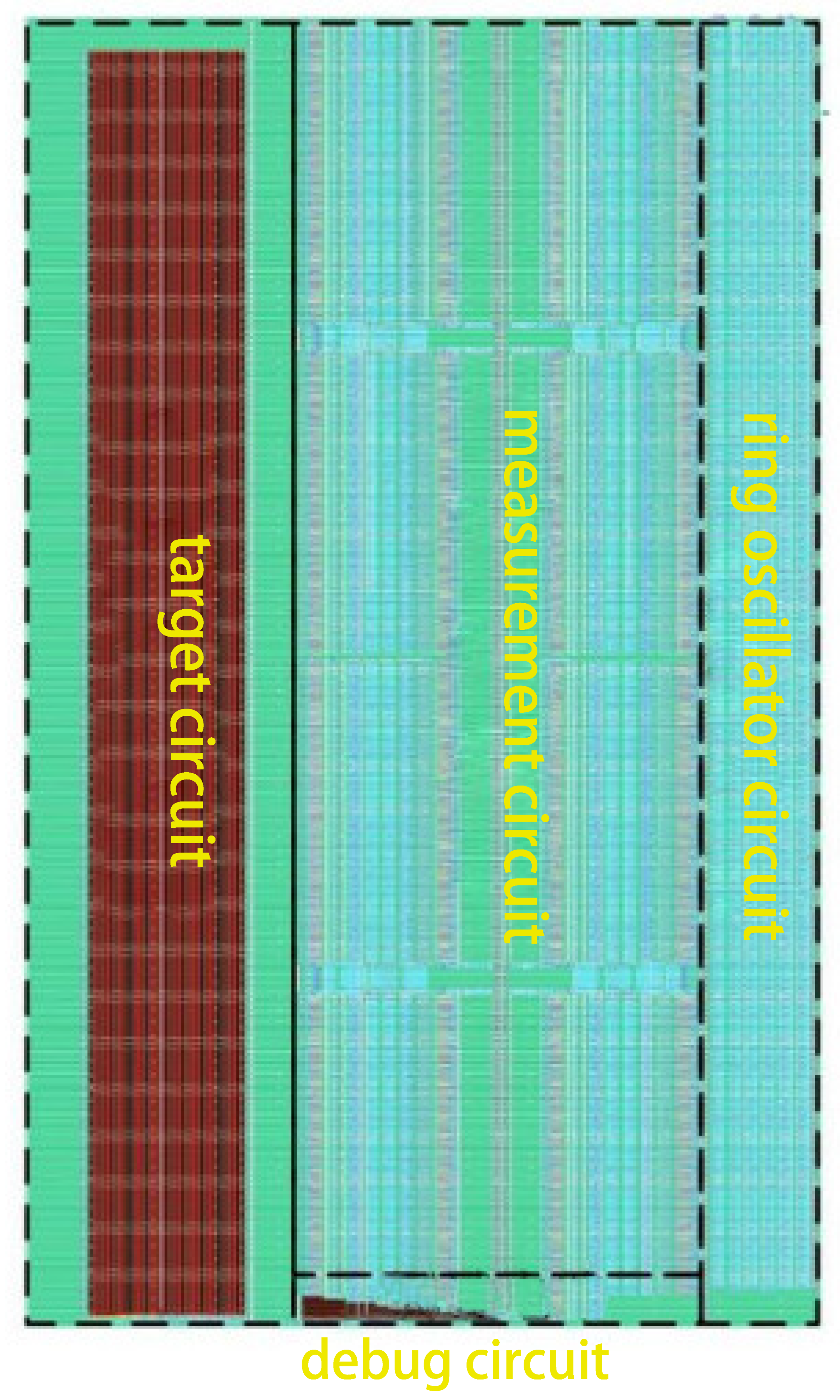
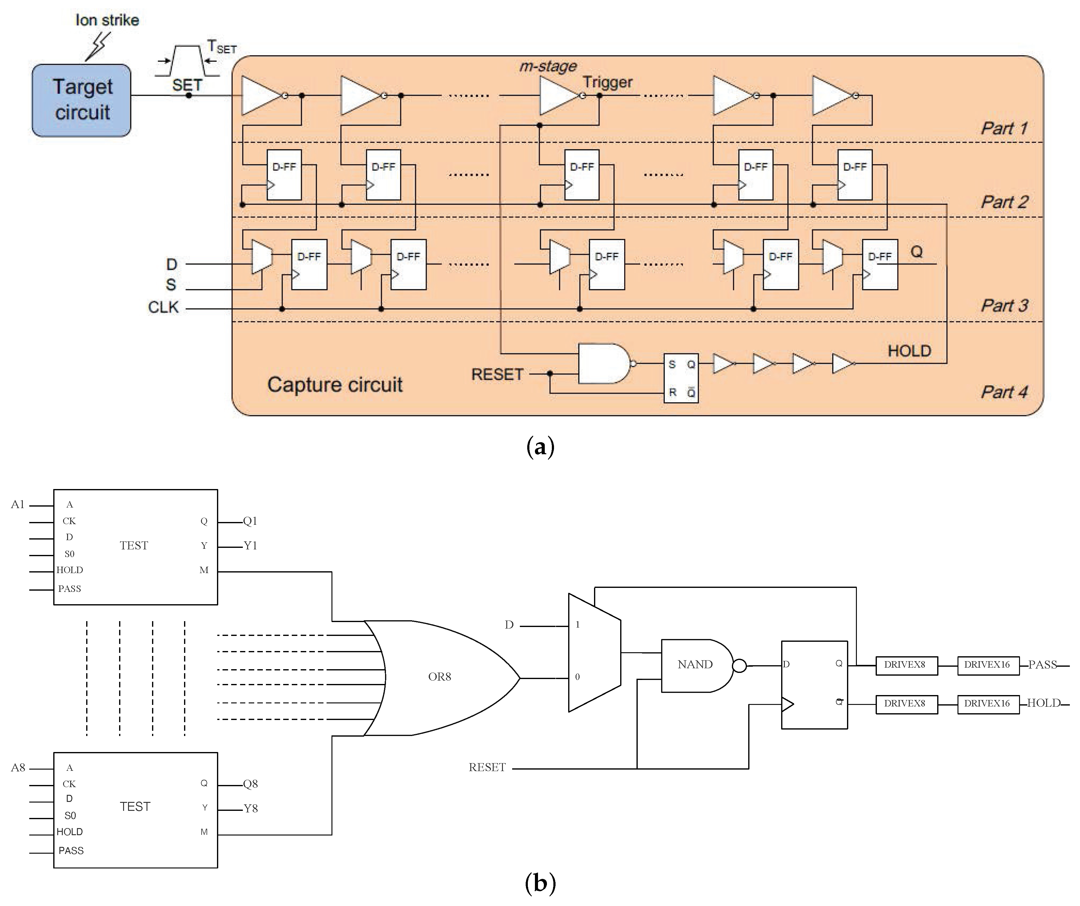
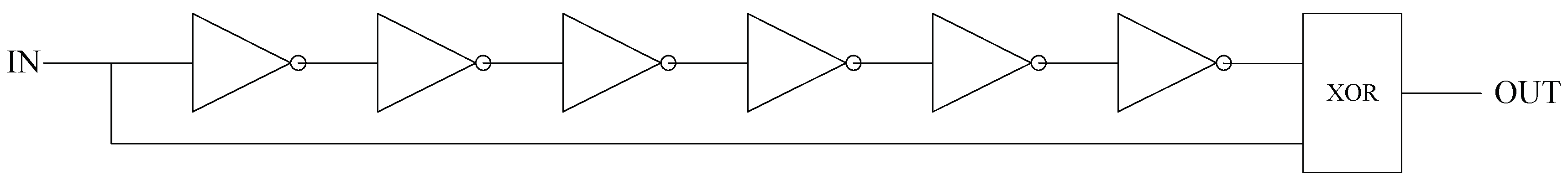
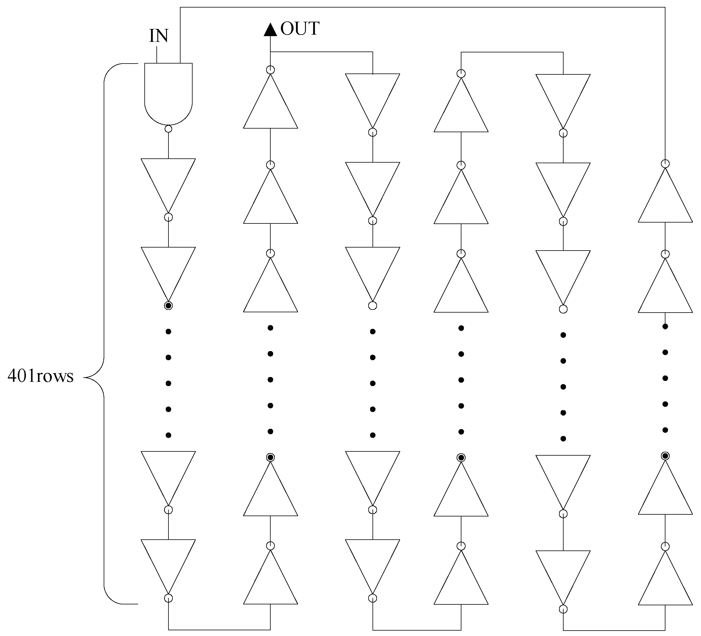
2. Test Chip Structure

The test chip consisting of four regions was developed as shown in Figure 1, which includes a target circuit, a measurement circuit, a debug circuit, and a ring oscillator circuit. SET generates in the target circuit (TC). TC is the same in structure as the target circuit of Reference [8]. The 800-level inverter chain is divided into 4200-level short chains and connected to the measurement circuit through the OR4 gate. Compared with a single long chain, such a structure can reduce the effect of propagation-induced pulse broadening (PIPB) effect. In the experiment, 32,200-level inverter chains were designed and divided into 8 groups, as shown in Figure 2. All inverters in any 200-level chain are placed vertically and the space between each two adjacent chains is the same, that is, 220 nm. The W/L of PMOS and NMOS is 255 nm/35 nm and 120 nm/35 nm, respectively.
The measurement circuit (MC) is shown in Figure 3, which is almost the same as the measurement structure in Reference [8]. The difference is that the inverter chain in part 1 of measurement circuit is appropriately extended to 190 stages, and the trigger position is set at the 120th stage inverter. 8 basic measurement circuits shown in (a) use the common self-trigger structure shown in (b) (instead of part 4 in (a)). The 8 SET measurement circuits are symmetrical about the x-axis and y-axis centers in the layout. The common self-trigger structure is placed in the middle of the layout to ensure that the delay of the “HOLD” signal reaching each SET measurement circuit matches.
The debug circuit (DC) consists of an even-numbered inverter chain and an exclusive-OR gate. Its circuit structure is shown in Figure 4. When the input signal “IN” changes, signal “OUT” will output a pulse with the width of the delay of the inverter chain, So changing the number of stages in the inverter chain can change the output pulse width. The designed test chip has a total of 8 sets of debug circuits, which are connected to 8 sets of SET measurement circuits. The number of stages of inverter chains in each set of debug circuits is shown in Table 1, the minimum number of inverter chain stages is 6 (the corresponding pulse width is about 60 ps) and the maximum is 40 (The corresponding pulse width is about 400 ps). The function of the debugging circuit is to simulate the transient pulse generated by the radiation, which is convenient for the function debugging of the test chip.
The delay of the inverter in the measurement circuit determines the accuracy of the measurement. Due to the existence of process variations, the delay of the inverter obtained in simulation is not the same as the delay of the inverter in actual experiments. The ring oscillator circuit (ROC) is used to measure the delay of a single inverter in actual experiments. ROC consists of a NAND gate unit and an inverter chain. The inverter unit used is the same as the inverter unit used in the inverter chain in the measurement circuit (MC). Figure 5 is a block diagram of a ROC. The low level of signal “IN” input can give an initial state to the ring oscillator circuit. After “IN” is maintained at a high level, the NAND gate unit is equivalent to an inverter unit. “OUT” outputs a square wave signal generated by oscillation. The designed ROC has a total of 2405 levels (including the NAND gate when the input IN = 1), then the output square wave frequency can be measured by the oscilloscope, so the delay of a single inverter stage can be calculated by the following formula:
Δ T = 1 2 × N × f
where N and f are the number of inverters of the ROC and the frequency measured at the OUT port, respectively.

3. Experimental Setup

The test chip is manufactured using a commercial 28 nm bulk silicon process, using a double well structure, and the total designed area is 63 × 501 μ m 2 . The test chips work at room temperature with the supply voltage of 0.9 V. Heavy ion experiments were performed on the Heavy Ion Accelerator Laboratory of the Institute of Modern Physics, Lanzhou Chinese Academy of Sciences and the HI-13 Tandem Accelerator of the Chinese Academy of Atomic Energy. As shown in Table 2, 5 kinds of heavy ions were used. The linear energy transfer (LET) value of Si ion is the smallest, which is 9.0 MeV · cm 2 · mg 1 , and the LET value of Ta ion is the largest, which is 81.35 MeV · cm 2 · mg 1 . The flux used in the experiments are relatively mild with 1 × 10 4 ions · cm 2 · s 1 or 2 × 10 4 ions · cm 2 · s 1 , the collected SETs are captured in real time in the experimental environment.
In addition, before and after each heavy ion experiment, the frequency of the ring oscillator circuit is tested with an oscilloscope, because it is important to calculate the true SET pulse width. The debug circuit is also used to judge whether the circuit is working properly before the test is officially started.

4. Experimental Results

4.1. Inverter Delay and Broadening Factor

By measuring the frequency of the ring circuit in each experiment with the oscilloscope, it is easy to calculate the delay of each stage of the inverter chains. In a total of 5 experiments, the frequency of the ring oscillation circuit does not change much and is basically stable at 26.6 MHz. Therefore, the stage delay of the inverter calculated by Formula (1) is 7.8 ps.
When the debug mode is enabled, the square pulse generated by the debug circuit is captured by the measurement circuit, so the pulse width generated in each debug circuit is also recorded, and the measured pulse width is found to be constant after multiple experimental measurements. The captured pulse widths are shown in Table 3. According to the 7.8 ps delay of each stage of the inverter and the number of inverters of each debugging circuit, the pulse width generated by each debugging circuit can be known, that is, the expected pulse width. According to the data recorded in the database in the experimental system, find the number of inverters that each pulse propagates through the 190-level inverter chain of the measurement circuit when the “Trigger” is triggered. Therefore, the average value of the broadening factor of the pulse broadening effect caused by the propagation is calculated to be 0.122 ps/stage. Although the results calculated by this method are not particularly accurate, they also have certain reference value. It was also found that SET was not captured in the shortest debug circuit because the measurement circuit had a certain minimum measurement threshold. This means that the measurement circuit cannot measure SET pulses lower than 46.8 ps.

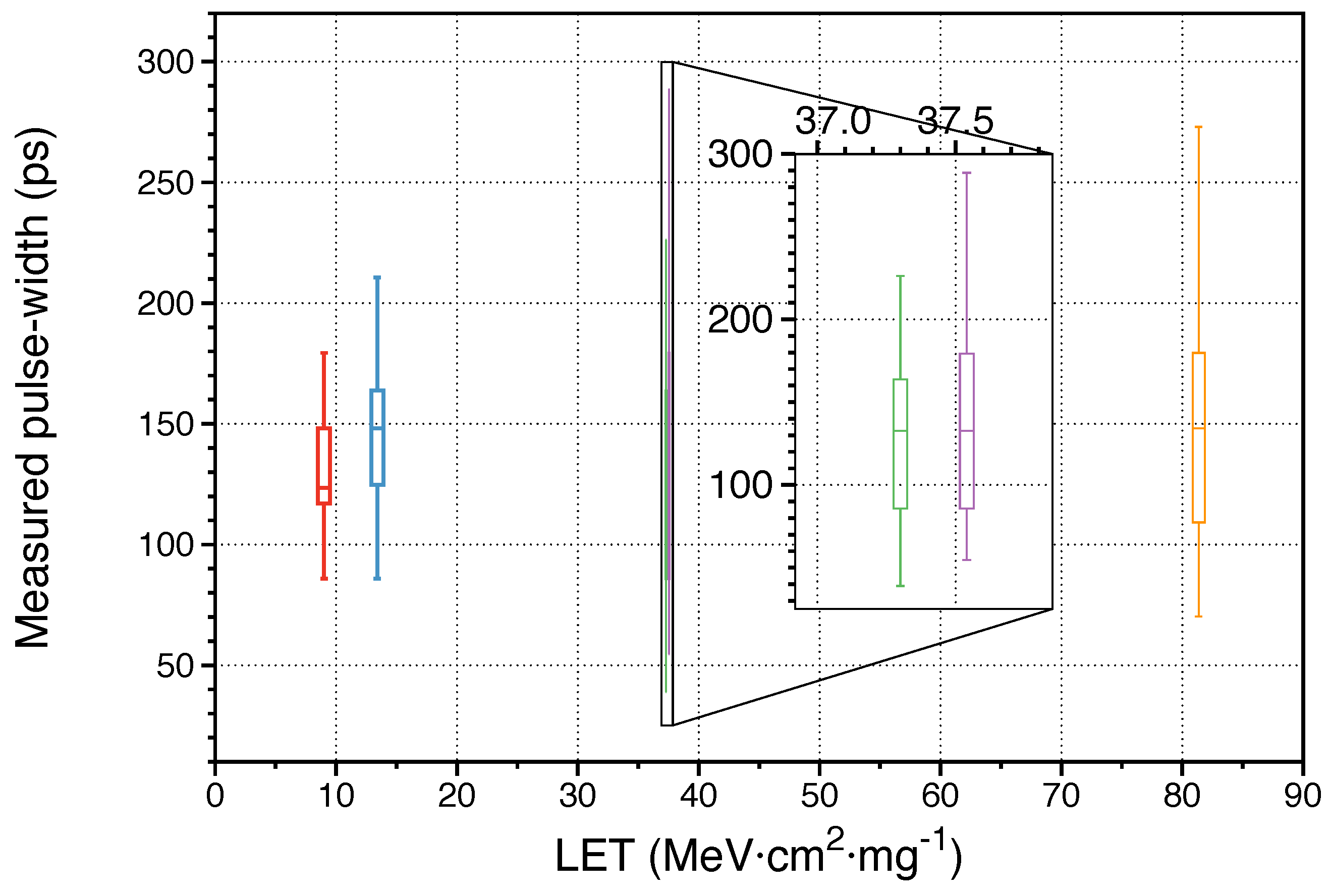
4.2. SET Characterization

A total of 5 different types of heavy ions with different energies were used in the radiation experiment. Table 2 lists their ion information in detail. For all ions, experiments with normal incidence have been performed. Although there is a certain difference in flux, it has no effect on the calculation of SET cross-section. Under different ion irradiation, the SET pulse width distribution and the SET cross-section are different. In Figure 6, the measured cross section for transients is plotted as the function of LET. Compared with the case [6] reported at 65 nm process, the SET cross section is smaller in 28 nm process, which is due to the smaller sensitive volume. When LET is more than 13.4 MeV · cm 2 · mg 1 , the cross-section of 65 nm process is more than an order of magnitude larger than 28 nm process, because of the reduction in sensitive volume. But at lower LET, the effect of critical charge required by generating SET exceeds the effect of sensitive volume, that means less deposited charge can also trigger transient pulses. It is foreseeable that the LET threshold of SET generated under advanced processes will be lower.
The distribution of pulse width as the function of LET is shown in Figure 7. With higher LET, the range of SET pulses is larger, which may depend on whether the ion impacts inside the drain (drift collection) or outside the drain (diffusion). When the LET value is approximately equal to 37 MeV · cm 2 · mg 1 (the Ge and Kr ions), the minimum pulse width measured is 54.6 ps, which is the same as the measurement threshold of the measurement circuit obtained in the debug circuit, and the count of minimum pulse width is not a few, it is very likely there are also many smaller transient pulses that have not been captured. The average pulse widths measured under different LET are similar as shown in Table 4, which also proves that smaller deposited charges in advanced processes are sufficient to trigger SET, and because at higher LET, more charges will be deposited, in the same well, it is very likely that charge sharing between the closely spaced transistors will cause multiple transient pulses or pulse compression effects, which are related to the electrical connection relationship. In this experiment, when using Ta ion to irradiate, 10% double transient pulses were observed, even if the interval between adjacent transistors is 220 nm, which is much larger than the minimum distance specified in the design rule check (DRC) file.

5. Discussion

In this article, the SET caused by heavy ions in the inverter chain in a 28 nm bulk silicon process is investigated. In the measurement process, we should pay attention to the measurement accuracy of the measurement circuit itself, that is, the stage delay of the inverter. In order to more accurately obtain the delay of the inverter chain in the measurement circuit, future experiments should try to construct it directly as a ring oscillator. A transient pulse of a certain width is artificially generated and captured by a measurement circuit. By comparing the output value of the measurement circuit with the artificially set input value, you can obtain the accurate measurement circuit’s measurement threshold. Spreading or compression of the input pulses for better correction of measurement results.
Experimental results show that the measurement threshold and resolution of this pulse measurement circuit are improved compared to similar measurement circuits in the 65 nm process, but still cannot fully contain pulses with smaller widths. Three types of measurement circuits are compared in Reference [6], the measurement structure which is called “Vernier” makes its resolution not directly limited by the combination gate delay, which should be a feasible solution in advanced technology.
The single-event multiple transient (SEMT) effect in the smaller transistor process cannot be ignored. Since we used the measurement structure proposed in Reference [8], single-event dual-transient data was also measured at a maximum LET value equal to 81.35 MeV · cm 2 · mg 1 , when the distance between adjacent transistors in the same well is increased, the situation will become worse in actual circuits. At the same time, low-energy ions in space may also bring more damage factors to existing single-event effect reinforcement methods and pose additional challenges.

6. Conclusions

Under the advanced technology, the influence of the reduction of the sensitive volume and the decrease of the critical charge on the production of SET is a competitive relationship. In 28 nm process, when LET is higher than 13.4 MeV · cm 2 · mg 1 , the reduction of the sensitive volume causes SET cross section to be more than an order of magnitude smaller than the data at 65 nm, but when LET is lower, reduced critical charge makes it easier for low-energy ions to induce transient pulses, so the SET cross section is close to the data in 65 nm. Measured smallest SET pulse width is 54.6 ps and is determined by minimum measurable value of measurement structure, which is 46.8 ps. With the reduction of clock frequency due to process shrinkage, the impact of smaller pulses must also be considered, and the multi-transients cannot be ignored. In future work, we can focus on the impact of small pulses on complex circuits and improve transient pulse measurement technology. In the case of multiple transients, the broadening and convergence of pulses may cause the original radiation-hardened design method to fail, which will bring more challenges.

Author Contributions

Writing—original draft, A.W.; Software, A.W. and Y.C.; Resources, B.L. and Y.C.; Writing—review and editing, A.W. and Z.W.; Project administration and funding acquisition, B.L. All authors have read and agreed to the published version of the manuscript.

Funding

This research was funded by the National Natural Science Foundation of China, grant number 61974163.

Acknowledgments

The authors would like to thank G. Guo, J. Liu, and the other members at the HI13 tandem accelerator in China Institute of Atomic Energy, Beijing, for heavy-ion tests. They thank the Lanzhou Heavy Ion Accelerator National Laboratory for heavy-ion testing support. They would also like to thank R. Sun, and X. Yao in the National University of Defense Technology, Changsha, China, for preparing the experiments.

Conflicts of Interest

The authors declare no conflict of interest.

References

  1. Dodd, P.; Shaneyfelt, M.; Schwank, J.; Felix, J. Current and future challenges in radiation effects on CMOS electronics. IEEE Trans. Nucl. Sci. 2010, 57, 1747–1763. [Google Scholar] [CrossRef]
  2. Ferlet-Cavrois, V.; Massengill, L.W.; Gouker, P. Single event transients in digital CMOS—A review. IEEE Trans. Nucl. Sci. 2013, 60, 1767–1790. [Google Scholar] [CrossRef]
  3. Song, R.; Shao, J.; Liang, B.; Chi, Y.; Chen, J. Characterization of P-hit and N-hit single-event transient using heavy ion microbeam. IEICE Electron. Express 2019. [Google Scholar] [CrossRef] [Green Version]
  4. Huang, P.; Chen, S.; Chen, J. Single event upset induced by single event double transient and its well-structure dependency in 65-nm bulk CMOS technology. Sci. China Inf. Sci. 2016, 59, 042411. [Google Scholar] [CrossRef]
  5. Andjelkovic, M.; Petrovic, V.; Nenadovic, M.; Breitenreiter, A.; Krstic, M.; Kraemer, R. Design of an On-chip System for the SET Pulse Width Measurement. In Proceedings of the 2017 Euromicro Conference on Digital System Design (DSD), Vienna, Austria, 30 August–1 September 2017; pp. 111–118. [Google Scholar]
  6. Glorieux, M.; Evans, A.; Ferlet-Cavrois, V.; Boatella-Polo, C.; Alexandrescu, D.; Clerc, S.; Gasiot, G.; Roche, P. Detailed SET measurement and characterization of a 65 nm bulk technology. IEEE Trans. Nucl. Sci. 2016, 64, 81–88. [Google Scholar] [CrossRef]
  7. Chen, R.; Chen, W.; Guo, X.; Shen, C.; Zhang, F.; Zheng, L.; Zhao, W.; Ding, L.; Luo, Y.; Guo, H.; et al. Improved on-chip self-triggered single-event transient measurement circuit design and applications. Microelectron. Reliab. 2017, 71, 99–105. [Google Scholar] [CrossRef]
  8. Huang, P.; Chen, S.; Chen, J.; Liang, B.; Chi, Y. Heavy-ion-induced charge sharing measurement with a novel uniform vertical inverter chains (UniVIC) SEMT test structure. IEEE Trans. Nucl. Sci. 2015, 62, 3330–3338. [Google Scholar] [CrossRef]
  9. Evans, A.; Glorieux, M.; Alexandrescu, D.; Polo, C.B.; Ferlet-Cavrois, V. Single event multiple transient (SEMT) measurements in 65 nm bulk technology. In Proceedings of the 2016 16th European Conference on Radiation and Its Effects on Components and Systems (RADECS), Bremen, Germany, 19–23 September 2016; pp. 1–6. [Google Scholar]
  10. Zhao, W.; He, C.; Chen, W.; Chen, R.; Cong, P.; Zhang, F.; Wang, Z.; Shen, C.; Zheng, L.; Guo, X.; et al. Single-event multiple transients in guard-ring hardened inverter chains of different layout designs. Microelectron. Reliab. 2018, 87, 151–157. [Google Scholar] [CrossRef]
  11. Benedetto, J.; Eaton, P.; Mavis, D.; Gadlage, M.; Turflinger, T. Digital single event transient trends with technology node scaling. IEEE Trans. Nucl. Sci. 2006, 53, 3462–3465. [Google Scholar] [CrossRef]
  12. Narasimham, B.; Bhuva, B.L.; Schrimpf, R.D.; Massengill, L.W.; Gadlage, M.J.; Amusan, O.A.; Holman, W.T.; Witulski, A.F.; Robinson, W.H.; Black, J.D.; et al. Characterization of digital single event transient pulse-widths in 130-nm and 90-nm CMOS technologies. IEEE Trans. Nucl. Sci. 2007, 54, 2506–2511. [Google Scholar] [CrossRef]
  13. Gadlage, M.J.; Ahlbin, J.R.; Narasimham, B.; Bhuva, B.L.; Massengill, L.W.; Reed, R.A.; Schrimpf, R.D.; Vizkelethy, G. Scaling trends in SET pulse widths in sub-100 nm bulk CMOS processes. IEEE Trans. Nucl. Sci. 2010, 57, 3336–3341. [Google Scholar] [CrossRef]
  14. Ahlbin, J.; Gadlage, M.; Ball, D.; Witulski, A.; Bhuva, B.; Reed, R.; Vizkelethy, G.; Massengill, L. The effect of layout topology on single-event transient pulse quenching in a 65 nm bulk CMOS process. IEEE Trans. Nucl. Sci. 2010, 57, 3380–3385. [Google Scholar] [CrossRef]
  15. Zhang, J.; Chen, J.; Huang, P.; Li, S.; Fang, L. The Effect of Deep N+ Well on Single-Event Transient in 65 nm Triple-Well NMOSFET. Symmetry 2019, 11, 154. [Google Scholar] [CrossRef] [Green Version]
  16. Chi, Y.; Song, R.; Shi, S.; Liu, B.; Cai, L.; Hu, C.; Guo, G. Characterization of single-event transient pulse broadening effect in 65 nm bulk inverter chains using heavy ion microbeam. IEEE Trans. Nucl. Sci. 2016, 64, 119–124. [Google Scholar] [CrossRef]
  17. Li, H.; Wu, L.; Yang, B.; Jiang, Y. Analysis of single event transient pulse-width in 65 nm commercial radiation-hardened logic cell. J. Semicond. 2017, 38, 085009. [Google Scholar] [CrossRef]
  18. Mitrović, M.; Hofbauer, M.; Goll, B.; Schneider-Hornstein, K.; Swoboda, R.; Steindl, B.; Voss, K.O.; Zimmermann, H. Experimental investigation of single-event transient waveforms depending on transistor spacing and charge sharing in 65-nm CMOS. IEEE Trans. Nucl. Sci. 2017, 64, 2136–2143. [Google Scholar] [CrossRef]
  19. Ferlet-Cavrois, V.; Paillet, P.; McMorrow, D.; Torres, A.; Gaillardin, M.; Melinger, J.; Knudson, A.; Campbell, A.; Schwank, J.; Vizkelethy, G.; et al. Direct measurement of transient pulses induced by laser and heavy ion irradiation in deca-nanometer devices. IEEE Trans. Nucl. Sci. 2005, 52, 2104–2113. [Google Scholar] [CrossRef]
  20. Narasimham, B.; Ramachandran, V.; Bhuva, B.L.; Schrimpf, R.D.; Witulski, A.F.; Holman, W.T.; Massengill, L.W.; Black, J.D.; Robinson, W.H.; McMorrow, D. On-chip characterization of single-event transient pulsewidths. IEEE Trans. Device Mater. Reliab. 2006, 6, 542–549. [Google Scholar] [CrossRef] [Green Version]
Figure 1. Test chip overall layout with 4 regions.
Symmetry 12 00624 g001
Figure 2. Target circuit structure with 32 inverter chains divided into groups every 4 chains.
Symmetry 12 00624 g002
Figure 3. The measurement circuit: (a) The basic measurement circuit. (b) With shared self-trigger structure.
Symmetry 12 00624 g003
Figure 4. Debug circuit structure with 6 inverters and an exclusive-OR gate.
Symmetry 12 00624 g004
Figure 5. Ring oscillator circuit structure with a NAND gate and an inverter chain.
Symmetry 12 00624 g005
Figure 6. Measured single-event transients (SET) cross-section as the function of linear energy transfer (LET) and research data in 65 nm.
Symmetry 12 00624 g006
Figure 7. Pulse width distribution of measured SET as the function of LET.
Symmetry 12 00624 g007
Table 1. The number of stages of inverter chains in each set of the debug circuit (DC).
DC Sets.Num.12345678
Stages.Count610162026303640
Table 2. Heavy ions used in the experiments.
IonEnergy
[MeV]
Incident Range
[ μ m]
LET
[ MeV · cm 2 · mg 1 ]
Flux
[ ions · cm 2 · s 1 ]
Fluence
[ ions · cm 2 ]
28Si12+14354.59.0 2 × 10 4 1 × 10 7
35Cl13+15042.813.4 2 × 10 4 1 × 10 7
74Ge19+20830.337.3 2 × 10 4 1 × 10 7
86Kr26+482.758.837.54 1 × 10 4 2 × 10 7
181Ta31+1400.883.381.35 1 × 10 4 5.6 × 10 6
Table 3. The number of stages of inverter chains in each set of DC.
DC Sets.Num.12345678
Expected pulse-width [ps]46.878124.8156202.8234280.8312
Captured pulse-width [ps]085.8132.6179.4226.2257.4304.2335.4
Passed INV count0150156156152152156158
Broadening factor [ps/stage]00.0520.0500.1500.1530.1530.1500.148
Table 4. Average pulse width of measured SET.
LET [ MeV · cm 2 · mg 1 ]9.013.437.337.5481.35
Average width [ps]128.7130.6131.4139.4154.7

