Abstract
The steady-state electrical conduction current for single and multilayer polyimide (PI) nanocomposite films was observed at the low and high electric field for different temperatures. Experimental data were fitted to conduction models to investigate the dominant conduction mechanism in these films. In most films, space charge limited current (SCLC) and Poole–Frenkel current displayed dominant conduction. At a high electric field, the ohmic conduction was replaced by current–voltage dependency. Higher conduction current was observed for nanocomposite films at a lower temperature, but it declined at a higher temperature. PI nanocomposite multilayer films showed a huge reduction in the conduction current at higher electric fields and temperatures. The conclusions derived in this study would provide the empirical basis and early breakdown phenomenon explanation when performing dielectric strength and partial discharge measurements of PI-based nanocomposite insulation systems of electric motors.
1. Introduction
Polyimide (PI) films are a widely used insulating material for engineering industries. These thin films are mainly used in electronic devices, multilayer surface coatings on metals, coatings on intermetallic compounds, temperature protection blankets in space crafts and magnetic wire enamelling for electric motor insulation [1,2]. PI thin films are also used for sensor coatings and composite electrodes for batteries [3,4,5,6,7,8]. PI nanocomposite films have also been studied and reported in different well-reputed research articles [9,10,11,12]; however, among these well-documented research articles, most of the focus is on the electrical breakdown strength related to the charge trapping and de-trapping mechanism and mechanical breakdown strength [13,14,15,16,17,18]. Despite this, very few studies are reported in relation to the early breakdown phenomenon in these films.
Over the last decade, nanodielectric insulating materials have received a lot of attention in the global market [19,20,21,22]. Several published studies proclaim that polymers and their derived nanocomposite insulating materials can enhance the dielectric properties for electrical applications [23,24,25,26,27,28,29]. In another study, fluorine-coated PI films have shown promising improvements in results by applying a thin layer of conductive surface coating on the top and bottom of these films [30,31]. These huge improvements in dielectric properties are conditioned on a better dispersion and interface region of nanoparticles, which is not easy to achieve, because these tiny particles can easily agglomerate. Other conditions necessary to obtain better results from these polymer-based nanocomposite materials are the structure of the composite and the size and type of nanoparticles being carefully selected and dispersed. Initially, it seemed as though nanoparticles were highly effective at improving the polymer’s properties; this would later be proven wrong after discerning the correct chemistry and mechanism of polymer-based nanocomposites. However, nanoparticles can enhance the polymer’s properties if important parameters, as mentioned above, are considered. The potential for these advancements has motivated us to improve the dispersion of nanoparticles and dielectric properties by synthesizing the multilayer structure. Therefore, we further explored those mechanisms in this research field using experimental and simulation work.
Conduction Current Theory
The sum of all conduction currents gives us a complete polarization current, which can be given as Equation (1) [32,33,34] where ii is the instant current, ia denotes the dipoles’ relaxation current and ic is the impurities conductivity current.
We can use Equation (2) to describe the conduction phenomenon. The time needed to obtain the steady-state current relies on the material’s nature, the applied electric field and the temperature. Normally, at higher temperatures and electric fields, the steady state is achieved earlier.
where ni is the concentration of charge carriers, qi are the fundamental charges and μi represents the respective charge carrier’s mobility. Under the electric field, the charge carrier moves either in the direction of the field or the opposite direction, depending on the dominant carrier polarity. For higher temperatures, the charge carriers and the charge mobility increase because the molecular motion increases with temperature. So, the following Arrhenius law from Equation (3) can describe the relationship between charge density, mobility and specific temperature T:
where EA is the thermal activation energy and k is the Boltzmann constant. According to this law, the conductivity increases with the increase in temperature. The field strength can also affect the density and mobility of the carriers, though it is generally believed that it is true only for electrons. The measurement of conductivity as a function of field strength provides a way to distinguish between mechanisms controlled primarily electronically and secondly by ions or dipoles [34,35]. The electrical conductivity increases with the increase in temperature and electric field, but, at the same time, it can be limited by the presence of intrinsic space charges because intrinsic charges can be understood as traps for the moving charges [36,37]. If homocharges are injected at the interface between the dielectric and the metal electrode, the local field is lowered, determining an increase in injection phenomena. Mott and Gurney have proved that the maximum current density J that corresponds to the space charge saturation (filled traps) inside the material, in a perfect dielectric without intrinsic carriers and without electron holes, will be given by Equation (4) [38].
This equation is valid only if the internal field completely cancels the electric field at the interface between the dielectric and the metal due to space charges. If the interfacial field is present, then the maximum current density J will be from Equation (5),
where x0 is the number of free electrons at the anode. For the case of a perfect dielectric, if the external field is low, the current density has an ohmic behavior, as presented in Equation (6).
If we compare the previous case with that of perfect insulation, the current density will be reduced with a specific factor θ, which corresponds to the fraction of carriers that are injected and trapped in the dielectric, as shown in Equation (7).
In the case of trapped charges, the depth level of the trapped charges also needs to be considered [39,40]. If the sample contains only one level of charge traps, the transition between the ohmic conduction and the space charge limited conduction is possible under the influence of a high field, due to part of the injected charges being trapped. However, when all the charge traps are filled, for a specific electric field (given by the trap filled region applied voltage VTFR), a sudden increase in current will be observed because the current will tend to approach the current density of material without traps. The two phenomena may be repeated if the material has several trap levels. The value of the VTFR voltage is given by Equation (8),
where nt represents the density of the traps found in the material. The polarization current for the samples increases as the electric field increases because the charge injection and the charge mobility depend on the electric field. The presence of a space charge inside the bulk of the samples can act as traps for the moving charges and limit the charge transport phenomena. Two phenomena can be used to describe the conduction for dielectric materials: the Poole–Frenkel effect and the space charge limited current (SCLC) [37,41]. Suppose that the applied electric field is low and the charge injection is neglected. In that case, as Coelho explains, the variation in the current density (J) concerning the electric field (E) corresponds to an ohmic behavior [34,42,43]. As the applied electric field increases, the type of conduction changes after a certain threshold voltage. The initial ohmic conduction is changed to space charge conduction, which depends on the trapped charges’ depth. When all the charge traps are filled, a sudden increase in current should be observed for a specific electric field, and the current will tend to reach the current density of material without traps [44]. The schematic diagram of conduction current J vs. E is presented in Figure 1.
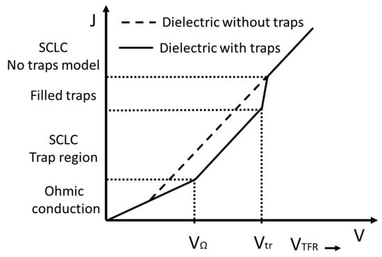
Figure 1.
Conduction current density vs. voltage.
2. Experimental Section
2.1. Sample Synthesis Procedure
The polymer chain can be obtained by reacting two monomers. In our case, we obtained Polyamic Acid (PAA) by reacting two monomers—diamine (ODA) and Pyromellitic dianhydride (PMDA)—in dipolar aprotic solvents, such as N-methyl pyrrolidone (NMP) or N, N-dimethylacetamide (DMAC), which later transformed into the final PI films by applying thermal imidization to PAA solution from 60 °C to 300 °C. The thermal and mechanical properties of PI can be altered by adopting several available monomers. During the reaction process, the percentage of ODA and PMDA can alter PAA’s molecular weight [43,45]. For PAA with a high molecular weight, it is important to dry the absorbed moisture from PMDA at 100 °C. First of all, ODA was put into the beaker and blended with DMAC for 30 min. The electromechanical system was used to stir the solution, then PMDA was blended into the mixture in two portions (first 90%, then the remaining 10%). It was mixed further for 8 to 10 h to obtain the final product of the PAA solution for PI films [45].
The PAA/SiO2 nanocomposite solution synthesis process is shown in Figure 2. The surface of SiO2 was modified by using the KH-550 coupling agent to produce the chemical linkage between organic PI and inorganic SiO2 nanoparticles. After modification, SiO2 nanoparticles were dried and blended with DMAC under ultrasonic waves for 30 min, then ODA was added and blended further for 60 min. Then, PMDA was mixed in two parts (90% and 10%) and blended for 6–8 h to get a yellow-colored nanocomposite-based PAA solution.
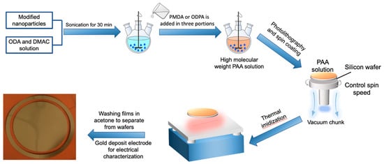
Figure 2.
Synthesis process of Polyamic Acid (PAA) solution. Polyimide (PI) films curing process using a spin coating technique and electrode deposition.
2.2. Spin Coating Technique to Cast PI Films
The spin coating technique was used to stake the PAA solution onto substrates [12]. Typically, a PAA solution is poured on the vacuum chunk substrate and rotated at high speeds of up to 6000 rpm. The control of the spinning speed helps to distribute the PAA solution to the entire surface homogenously. Two to three steps of speed rise can be used to allow the PAA solution to gradually cover more than 80% of the substrate before continuing on to the final speed. For multilayer PI/SiO2 films, two spinning speed levels were applied. After calibration, we applied 20 s at a speed of 500 rpm to obtain the first PI layer of 60 µm thickness, and then soft baked it for 30 min at 80 °C. Once the first layer was half cured on the silicon wafer, the nanoparticles-mixed PAA solution was then poured on the half-cured first layer and we placed the silicon wafer on the spin coating machine; a spin speed of 1000 rpm at 30 s was applied to obtain the second PI/SiO2 layer of 20–30 µm thickness [45].
2.3. PI Films Fluorination
An F2/N2 gas phase mixture with 12.5% F2 by volume at 0.1 MPa pressure and 40 °C temperature was used for 45 min in a laboratory-made stainless steel vessel to modify the surface on both sides of PI films. The thickness of the PI was 125 μm and the thickness of the fluorination coating was 0.5 to 1 μm [30,46,47]. Measured samples have deposition electrodes of 5 cm diameter on both sides.
2.4. Composition of Multilayer Films and SEM
Polyimide nanocomposites are thin nanofilms with complex chemical synthesis processes to achieve samples 100 microns or thicker. JEOL JSM 6460 and FEI inspect S50 SEM(JEOL, Tokyo, Japan) at CTM-IES of UM are used to scan PI and multilayer PI/SiO2 samples. Scattered secondary electrons are used in SEM for surface topography and composition of samples. In SEM, the sample is coated with a conductive material or pasted on conductive metals such as gold and aluminum. SEM can also provide surface roughness information of samples. The surface area, ranging from 1 cm to 5 µm, can be imaged in a SEM scanning mode with amplification from 20× to 30,000× and a spatial resolution of 50 to 100 nm. The surface topography of the PI/SiO2 single and multilayer films is shown in Figure 3. The SEM images in Figure 3a,c show nanoparticle dispersion for single-layer PI/SiO2 films while the right column, as shown in Figure 3b,d shows the multilayer PI/SiO2 structure. White regions in these figures correspond to the nanofiller inclusions and darker ones to the polyimide matrix. We observed a better nanoparticles dispersion in PI/SiO2 multilayer films, as shown in the right column SEM images of Figure 3b,d, compared with PI/SiO2 single-layer film with few nanoparticle agglomeration spots with the size of 550 nm, as shown in Figure 3a.
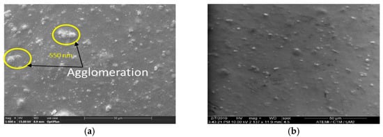
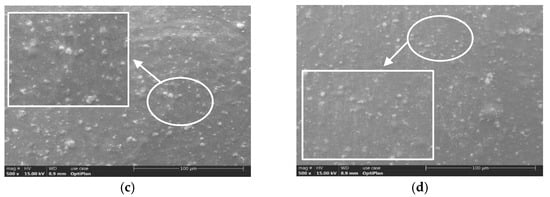
Figure 3.
SEM image of surface topography of single PI/SiO2 films (a,c) and multilayer PI/SiO2 nanocomposite films (b,d).
2.5. Measurements
The PI films with guard ring electrodes were fixed in a temperature-controlled chamber to measure the conduction current, as shown in Figure 4. The electric field (up to 50 kV/mm) was applied by a low residual ripple voltage power supply with a maximum limit of 35 kV High Voltage DC supply (Fug HCP140-35000). The quasi-steady-state polarization current, known as conduction current, was obtained after the transient regime of the absorption during 3000–5000 s, as shown in Figure 5. When we applied an electric field to the thin sample of PI films, there was slight current conduction through the samples. This current conduction can be due to various reasons [34,44] such as:
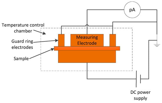
Figure 4.
Guard ring electrode setup to measure the conduction current.
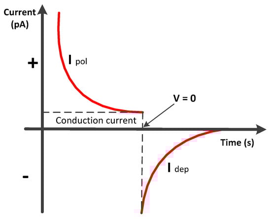
Figure 5.
I(t) characteristics of polarization and depolarization current.
- (1)
- the orientation of dipoles;
- (2)
- displacement of the positive and negative charges;
- (3)
- shifting of mobile positive and negative carriers (Maxwell-Wagner-Sillars polarization); and
- (4)
- space charge injection from electrodes and its accumulation in the bulk of the sample.
3. Results
For the studied conduction current of samples (films), the J vs. E graphs are plotted in Figure 6a–c. By analyzing these, we can observe an increase in conduction current in the case of fillers added in the polyimide matrix at low temperature, but we observe a conduction current decrease for nanocomposite samples at high temperature. All the films expose the same trend of conduction current profile at low electric fields (<16 kV/mm), in which the conductivity of single-layer PI/SiO2 and fluorinated samples (FPI) is higher than the pure PI and multilayer PI-PI/SiO2 films at low electric fields [47,48,49]. Higher conductivity can help to release trap charges [48,50,51]. As shown in Figure 6, we observed that the films have at least two to three types of conduction from the slope of the current density J, relying on the applied electric field and temperatures. An ohmic current is confirmed by a slope close to 1, corresponding to a linear change in the J vs. E plot. Generally, the ohmic current relates to the participation of the intrinsic charges in conduction. The charge injection is increased from electrodes at the higher electric field, and the ohmic conduction becomes current–voltage dependent.
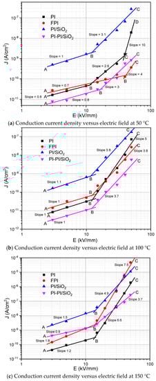
Figure 6.
Conduction current density versus electric field at different temperatures.
In this particular case, the dependence between the current density and the electric field confirmed by slopes higher than 1 is found. This behavior could be associated with the different conduction phenomena happening in the samples. It is interesting to observe that the single-layer PI/SiO2 samples’ current densities are the highest, whatever the electric field and temperature, while multilayer PI-PI/SiO2 samples show, in most of the cases, the lowest current densities—except 150 °C. This could demonstrate that the nanoparticles favor the charge flow when agglomerated and reduce charge flow when dispersing homogenously. After plotting the results in a log/log scale, as shown in Figure 6, we observed an ohmic current in most of the samples with slope ≤ 1 at low field, showing in the region AB. The applied threshold electric field of the order of 9 to 15 kV/mm, depending on the temperature, shows a nonlinearity in the conduction current rise with the slope > 1, indicating a nonohmic conduction mechanism.
The results shown in Figure 6 were further analyzed to find the dominant injection or conduction mechanism in all samples, such as space charge limited current (SCLC) and Poole–Frenkel conduction. The Schottky injection can occur due to electrons’ activation energy at the electrode/dielectric interface caused by lowering the energy barrier at the interface. The Poole–Frenkel emission belongs to the conduction due to the electron’s traps in the bulk of insulation. These trapped electrons can gain some activation energy to be de-trapped and participate in the conduction. Another conduction that can increase the nonlinearity (Slope ≥ 2) in J-E plots is due to the SCLC, which can be influenced by the traps. Therefore, these models can apply to the experimental results to explain the conduction mechanism. The results were analyzed using different representations of the conduction current density J concerning the applied electric field E. We divided the results into three regions (marked as AB, BC and CD) having different slopes, which implies that the J–E relation is of the type J ∝ En, where n is the curve slope. The ohmic regions at 50 °C, 100 °C and 150 °C are shown with the AB region in Figure 6.
In Figure 6c, but for FPI and PI/SiO2 films at 150 °C, the current density J is proportional to the square of the electric field in the first slope of region AB, which can be the characteristic of an SCLC regime, where the current density–electric field dependence is given by Equation (9) and plotted in Figure 7.
where µ is the carrier mobility, V is the applied voltage, d is the sample thickness, εr is the relative permittivity of the material and ε0 is the vacuum permittivity. The slope of the J vs. E2/d line should be 1 to confirm the SCLC conduction. Slope <1 in Figure 7 is in area AB, in which the dominant conduction mechanism is ohmic. Thus, it could not be the SCLC mechanism. Slope 1 in Figure 7 represents the trap-free SCLC, whereas slope >1 represents the trap-filled SCLC. Figure 7 shows that only for FPI and PI/SiO2 at 150 °C (a better fit for FPI rather than PI/SiO2) the slope equals 1, which confirms the SCLC in this region [34]. Thus, it appears that the SCLC mechanism is not the dominant mechanism demonstrated by our samples in the studied conditions.
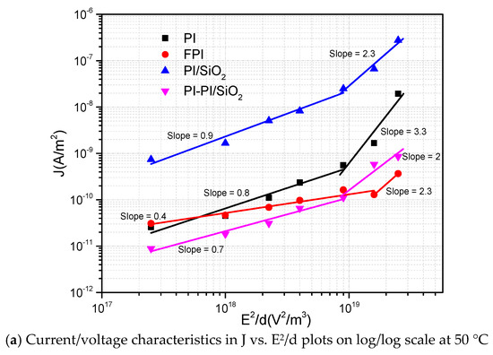
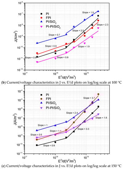
Figure 7.
Space charge limited current (SCLC) conduction mechanism at different temperatures.
To conclude, it seems that SCLC would only be present at 150 °C for FPI and PI/SiO2 specimens. The second slope for PI, FPI, PI/SiO2 and PI-PI/SiO2 films obtained at the high electric field has a higher value, which seems to correspond either to the trap-filled region or other conduction mechanisms. The second slope of PI film at 50 °C and the second slope of PI and FPI films at temperatures above 150 °C is higher than 2, which could correspond to other conduction mechanisms. The SCLC regime cannot explain the samples that have a slope region BC higher than 2. The chemical and physical composition of samples related to the glass transition may affect the conduction in these regions.
Thus, the conduction in these regions is mainly controlled by another mechanism. Other conduction mechanisms, such as Schottky and Poole–Frenkel, have to be considered as well. The Poole–Frenkel effect is a bulk conduction mechanism where the barrier between localized states is lowered due to the high electric field’s influence. The conductivity is given by Equation (10) [51].
where σ0 is the material’s intrinsic conductivity, βPF is the Poole–Frenkel constant defined in Equation (11), k is the Boltzmann constant and T is the absolute temperature. If this mechanism is dominant, the ln (J/E) plot versus E1/2 must be a straight line with a slope close to βPF/(kT).
The βPF coefficients are first calculated from the slope, then the dielectric constants are estimated from these coefficients using Equation (11). If these dielectric constants agree with the values cited in the literature, it could be said that the samples follow the corresponding conduction mechanism. Representations in ln (J/E) versus E1/2 coordinates are presented in Figure 8. These representations are not linear for FPI, PI/SiO2 and PI-PI/SiO2 films at 50 °C, and their dielectric constant is in the range of 6 to 15, which is higher than the measured one.
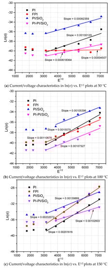
Figure 8.
Poole–Frenkel conduction mechanism at different temperatures.
The slopes of these representations are also not linear for PI, FPI and PI/SiO2 films at 150 °C, and their dielectric constant is in the range of 0.8 to 2.2, which is lower than the measured one as shown in Table 1. Therefore, Poole–Frenkel conduction seems not to be the case for these films; however, these representations can be seen to be linear for PI at 50 °C and linear for FPI, PI/SiO2 and PI-PI/SiO2 at 100 °C, and their values are close to the calculated βPF/(kT) values. It is also linear for multilayer PI-PI/SiO2 nanocomposite films at 150 °C, and their calculated dielectric constant from the model is close to the measured one, which could confirm Poole–Frenkel conduction in these films.

Table 1.
Comparison of slope value and calculated βPF/kT value at various temperatures.
4. Conclusions
Here, we summarize the possible conduction phenomena for all of the studied materials at different temperatures and the electric field ranges. At least one possible conduction of each class related to charge injection or bulk conduction should be present to describe the steady-state conduction current. Nonetheless, for some samples such as FPI and PI-PI/SiO2, two different conduction mechanisms from the same bulk conduction class seem to be present at a high temperature of 150 °C. SCLC relates to the mobility of holes and electrons, while other conductions relate to ion donors and acceptor sites present in bulk, which need thermal or electrical energy to participate in the conduction by giving their space to neighboring electrons or holes, depending on their trap energy level. We estimate these conduction phenomena by analyzing the slope of the current density over a certain range of electric field, not just a point. Thus, it seems difficult to consider that this conduction is happening exactly in this electric field. The study of conduction mechanisms in polymeric materials is not easy, and this is even more true when it concerns composite materials. It appears from this study that dominant conduction mechanisms are strongly dependent on the electric field and the measurement temperature, whatever the type of studied material. Nevertheless, in the materials of this study based on polyimides, we can say that two volume conduction mechanisms seem to be predominant at high temperatures.
Author Contributions
Conceptualization, M.S.B. and S.A. (Shakeel Akram); Methodology, M.S.B.; Software, M.S.B., S.A. (Shakeel Akram), P.M., H.L., G.R. and J.C.; Validation, P.M., H.L., G.R. and J.C.; Formal Analysis, M.S.B., S.A. (Shakeel Akram), H.L., Y.G. and S.A. (Shakeel Akram); Investigation, H.L., Y.G. and S.A. (Serge Agnel); Resources, P.M.; Data Curation, H.L., Y.G. and S.A. (Serge Agnel); Writing—Original Draft Preparation, M.S.B. and S.A. (Shakeel Akram); Writing—Review & Editing, S.H. and M.T.N.; Visualization, M.S.B., H.L. and Y.G.; Supervision, M.S.B., S.A. (Shakeel Akram) and P.M.; Project Administration, P.M.; Funding Acquisition, P.M. and M.T.N. All authors have read and agreed to the published version of the manuscript.
Funding
This work was supported by the National Natural Science Foundation of China under Grant No. 51407121.
Institutional Review Board Statement
Not applicable.
Informed Consent Statement
Not applicable.
Data Availability Statement
All data is included within the manuscript.
Conflicts of Interest
The authors declare no conflict of interest and that they have no known competing financial interests or personal relationships that could have appeared to influence the work reported in this paper.
References
- Akram, S.; Wang, P.; Nazir, M.T.; Zhou, K.; Bhutta, M.S.; Hussain, H. Impact of impulse voltage frequency on the partial discharge characteristic of electric vehicles motor insulation. Eng. Fail. Anal. 2020, 116, 104767. [Google Scholar] [CrossRef]
- Lai, G.-H.; Huang, T.-C.; Tseng, I.-H.; Huang, B.-S.; Yang, T.-I.; Tsai, M.-H. Transparency anticorrosion coatings prepared from alumina-covered graphene oxide/polyimide nanocomposites. Express Polym. Lett. 2019, 13, 772–784. [Google Scholar] [CrossRef]
- Sousa, J.; Marques, J.; Garcia, M.; Infante, V.; Amaral, P. Mechanical characterization of sandwich composites with embedded sensors. Eng. Fail. Anal. 2020, 117, 104765. [Google Scholar] [CrossRef]
- Lee, Y.-C.; Ahn, J.-H.; Lee, C.-Y. Grid-type sensors using resistance change ratio for micro-crack detection. Eng. Fail. Anal. 2021, 119, 104973. [Google Scholar] [CrossRef]
- Kronenberg, P.; Rastogi, P.K.; Giaccari, P.; Limberger, H.G. Relative humidity sensor with optical fiber Bragg gratings. Opt. Lett. 2002, 27, 1385. [Google Scholar] [CrossRef] [PubMed]
- Lin, D.; Liu, Y.; Cui, Y. Reviving the lithium metal anode for high-energy batteries. Nat. Nanotechnol. 2017, 12, 194–206. [Google Scholar] [CrossRef]
- Zhao, J.; Kang, T.; Chu, Y.; Chen, P.; Jin, F.; Shen, Y.; Chen, L. A polyimide cathode with superior stability and rate capability for lithium-ion batteries. Nano Res. 2019, 12, 1355–1360. [Google Scholar] [CrossRef]
- Palneedi, H.; Peddigari, M.; Hwang, G.-T.; Jeong, D.-Y.; Ryu, J. High-Performance Dielectric Ceramic Films for Energy Storage Capacitors: Progress and Outlook. Adv. Funct. Mater. 2018, 28, 1803665. [Google Scholar] [CrossRef]
- Akram, S.; Castellon, J.; Kai, Z.; Agnel, S.; Habas, J.-P.; Nazir, M.T. Dielectric properties and modeling of multilayer polyimide nanocomposite to highlight the impact of nanoparticles dispersion. IEEE Trans. Dielectr. Electr. Insul. 2020, 27, 1238–1246. [Google Scholar] [CrossRef]
- Akram, S.; Gao, G.; Liu, Y.; Zhu, J.; Wu, G. Degradation mechanism of A12O3 nano filled polyimide film due to surface discharge under square impulse voltage. IEEE Trans. Dielectr. Electr. Insul. 2015, 22, 3341–3349. [Google Scholar] [CrossRef]
- Akram, S.; Yang, Y.; Zhong, X.; Bhutta, S.; Wu, G.; Castellon, J.; Zhou, K. Influence of nano layer structure of polyimide film on space charge behavior and trap levels. IEEE Trans. Dielectr. Electr. Insul. 2018, 25, 1461–1469. [Google Scholar] [CrossRef]
- Akram, S.; Castellon, J.; Agnel, S.; Habas, J.-P. Synthesis Process Optimization of Polyimide Nanocomposite Multilayer Films, Their Dielectric Properties, and Modeling. In Polyimide for Electronic and Electrical Engineering Applications; IntechOpen: London UK, 2020. [Google Scholar]
- Haq, S.U. A Study on Insulation Problems in Drive Fed Medium Voltage Induction Motors. Ph.D. Thesis, Department of Electrical and Computer Engineering, University of Waterloo, Waterloo, ON, Canada, 2007. [Google Scholar]
- Kaufhold, M.; Aninger, H.; Berth, M.; Speck, J.; Eberhardt, M. Electrical stress and failure mechanism of the winding insulation in PWM-inverter-fed low-voltage induction motors. IEEE Trans. Ind. Electron. 2000, 47, 396–402. [Google Scholar] [CrossRef]
- Akram, S.; Nazir, M.T.; Castellon, J.; Agnel, S.; Zhou, K.; Bhutta, M.S.; Kai, Z. Preparation and distinguish dielectric properties of multi-layer nanoparticles-based polyimide films. Mater. Res. Express 2019, 6, 125092. [Google Scholar] [CrossRef]
- Yang, Y.; He, J.; Wu, G.; Hu, J. “Thermal Stabilization Effect” of Al2O3 nano-dopants improves the high-temperature dielectric performance of polyimide. Sci. Rep. 2015, 5, 1–10. [Google Scholar] [CrossRef] [PubMed]
- Bhutta, M.S.; Yang, L.; Ma, Z.; Nazir, M.T.; Akram, S.; Mehmood, M.A.; Faiz, N. Simulation of thickness controlled DC breakdown of XLPE regulated by space charge & molecular chain movement. IEEE Trans. Dielectr. Electr. Insul. 2020, 27, 1143–1151. [Google Scholar] [CrossRef]
- Meng, P.; Zhao, X.; Yang, X.; Wu, J.; Xie, Q.; He, J.; Hu, J.; He, J. Breakdown phenomenon of ZnO varistors caused by non-uniform distribution of internal pores. J. Eur. Ceram. Soc. 2019, 39, 4824–4830. [Google Scholar] [CrossRef]
- Nazir, M.T.; Phung, B.T.; Li, S.; Akram, S.; Mehmood, M.A.; Yeoh, G.H.; Hussain, S. Effect of micro-nano additives on breakdown, surface tracking and mechanical performance of ethylene propylene diene monomer for high voltage insulation. J. Mater. Sci. Mater. Electron. 2019, 30, 14061–14071. [Google Scholar] [CrossRef]
- Nazir, M.T.; Butt, F.T.; Phung, B.T.; Yeoh, G.H.; Yasin, G.; Akram, S.; Bhutta, M.S.; Hussain, S.; Nguyen, T.A. Simulation and Experimental Investigation on Carbonized Tracking Failure of EPDM/BN-Based Electrical Insulation. Polymers 2020, 12, 582. [Google Scholar] [CrossRef] [PubMed]
- Zhong, X.; Shakeel, A.; Yang, Y.; Gao, G.; Wu, G. Preparation and corona-resistance characteristics of double-layer polyimide/Al2O3 nanocomposite film. In Proceedings of the 2016 IEEE International Conference on High Voltage Engineering and Application (ICHVE), Chengdu, China, 19–22 September 2016; pp. 1–4. [Google Scholar] [CrossRef]
- Butt, F.T.; Nazir, M.T.; Hussain, H.; Phung, B.T.; Akram, S.; Bhutta, M.S.; Yasin, G. Physical, thermal and partial discharge evaluation of nano alumina filled silicone rubber in inclined plane test. CSEE J. Power Energy Syst. 2020. [Google Scholar] [CrossRef]
- Wang, P.; Hui, S.; Akram, S.; Zhou, K.; Nazir, M.T.; Chen, Y.; Dong, H.; Javed, M.S.; Haq, I.U. Influence of Repetitive Square Voltage Duty Cycle on the Electrical Tree Characteristics of Epoxy Resin. Polymers 2020, 12, 2215. [Google Scholar] [CrossRef]
- Bhutta, M.S.; Yang, L.; Ma, Z.; Ahmad, J.; Mehmood, M.A. Influence of Polyhedral Oligomeric Silsesquioxane (POSS) on Space Charge Behavior and Trap Levels of XLPE/POSS nanocomposite. In Proceedings of the 2018 IEEE 2nd International Conference on Dielectrics (ICD), Budapest, Hungary, 1–5 July 2018; p. 4. [Google Scholar]
- Meng, P.; Wu, J.; Yang, X.; Hu, J.; He, J. Electrical properties of ZnO varistor ceramics modified by rare earth-yttrium and gallium dopants. Mater. Lett. 2018, 233, 20–23. [Google Scholar] [CrossRef]
- Bokobza, L. Multiwall carbon nanotube-filled natural rubber: Electrical and mechanical properties. Express Polym. Lett. 2012, 6, 213–223. [Google Scholar] [CrossRef]
- Ghorpade, R.V.; Rajan, C.R.; Chavan, N.N.; Ponrathnam, S. Synthesis of novel silica-polyimide nanocomposite films using aromatic-amino modified silica nanoparticles: Mechanical, thermal and morphological investigations. Express Polym. Lett. 2015, 9, 469–479. [Google Scholar] [CrossRef]
- Hu, J.; Gu, A.; Liang, G.; Zhuo, D.; Yuan, L. Preparation and properties of mesoporous silica/bismaleimide/diallylbisphenol composites with improved thermal stability, mechanical and dielectric properties. Express Polym. Lett. 2011, 5, 555–568. [Google Scholar] [CrossRef]
- Spoljaric, S.; Shanks, R.A. Novel elastomer dye-functionalised POSS nanocomposites: Enhanced colourimetric, thermomechanical and thermal properties. Express Polym. Lett. 2012, 6, 354–372. [Google Scholar] [CrossRef]
- Akram, S.; Castellon, J.; Agnel, S.; Khan, M.Z. Space charge analysis of multi-structure polyimide films using TSM. In Proceedings of the IEEE Conference on Electrical Insulation and Dielectric Phenomena (CEIDP), Cancun, Mexico, 21–24 October 2018; pp. 34–37. [Google Scholar]
- Akram, S.; Zhou, K.; Meng, P.F.; Castellon, J.; Agnel, S.; Wang, P.; Nazir, M.T.; Chen, Y.; Hussain, H. Charge Transport and Trapping of Surface Modified Stator Coil Insulation of Motors. IEEE Trans. Dielect. Electr. Insul. 2021, in press. [Google Scholar]
- Castellon, J.; Nguyen, H.N.; Agnel, S.; Toureille, A.; Frechette, M.; Savoie, S.; Krivda, A.; Schmidt, L. Electrical properties analysis of micro and nano composite epoxy resin materials. IEEE Trans. Dielectr. Electr. Insul. 2011, 18, 651–658. [Google Scholar] [CrossRef]
- Diaham, S.; Saysouk, F.; Locatelli, M.-L.; Lebey, T. Huge improvements of electrical conduction and dielectric breakdown in polyimide/BN nanocomposites. IEEE Trans. Dielectr. Electr. Insul. 2016, 23, 2795–2803. [Google Scholar] [CrossRef]
- Yahyaoui, H.; Notingher, P.; Agnel, S.; Kieffel, Y.; Girodet, A. Analysis of conduction mechanisms in alumina-filled epoxy resin under dc field and temperature. In Proceedings of the 2013 Annual Report Conference on Electrical Insulation and Dielectric Phenomena, Shenzhen, China, 20–23 October 2013; pp. 667–670. [Google Scholar] [CrossRef]
- Bhumiwat, S.A. Advanced Applications of Polarisation/Depolarisation Current Analysis on Power Transformers. In Proceedings of the Conference Record of the 2008 IEEE International Symposium on Electrical Insulation, Vancouver, BC, Canada, 9–12 June 2008; pp. 474–477. [Google Scholar] [CrossRef]
- Zhu, Y.B.; Ang, L.K. Analytical re-derivation of space charge limited current in solids using capacitor model. J. Appl. Phys. 2011, 110, 094514. [Google Scholar] [CrossRef]
- Rose, A. Space-Charge-Limited Currents in Solids. Phys. Rev. 1955, 97, 1538–1544. [Google Scholar] [CrossRef]
- Mott, N.F.; Gurney, R.W. Electronic processes in ionic crystals. J. Phys. Chem. 1941, 45, 1142. [Google Scholar] [CrossRef]
- Chen, Y.; Wang, Y.; Wu, J.; Yin, Y. Study on conduction current characteristics of corona-resistant polyimide film before and after thermal aging. In Proceedings of the 2017 International Symposium on Electrical Insulating Materials (ISEIM), Toyohashi, Japan, 11–15 September 2017; Volume 2, pp. 605–608. [Google Scholar] [CrossRef]
- Ieda, M.; Mizutani, T.; Ikeda, S. Electrical Conduction and Chemical Structure of Insulating Polymers. IEEE Trans. Electr. Insul. 1986, -EI-21, 301–306. [Google Scholar] [CrossRef]
- Lan, L.; Wu, J.; Yin, Y.; Li, X.; Li, Z. Effect of temperature on space charge trapping and conduction in cross-linked polyethylene. IEEE Trans. Dielectr. Electr. Insul. 2014, 21, 1784–1791. [Google Scholar] [CrossRef]
- Fofana, I.; Hemmatjou, H.; Farzaneh, M.; Gockenbach, E.; Borsi, H. Polarization and Depolarization Current measurements of oil impregnated paper insulation system under thermal runaway. In Proceedings of the 2010 10th IEEE International Conference on Solid Dielectrics, Potsdam, Germany, 4–9 July 2010; pp. 1–4. [Google Scholar] [CrossRef]
- Dunson, D.L. Synthesis and Characterization of Thermosetting Polyimide Oligomers for Microelectronics Packaging. Ph.D. Thesis, Department of Chemistry, Virginia Polytechnic Institute and State University, Blacksburg, VA, USA, 2000. [Google Scholar]
- Akram, S.; Castellon, J.; Agnel, S.; Zhou, K.; Habas, J.-P.; Nazir, M.T. Multilayer polyimide nanocomposite films synthesis process optimization impact on nanoparticles dispersion and their dielectric performance. J. Appl. Polym. Sci. 2021, 138, 49715. [Google Scholar] [CrossRef]
- Critchley, P.; Knight, G.J.; Wright, W.W. Heat-Resistant Polymers: Technologically Useful Materials; Springer US: New York, NY, USA, 1983. [Google Scholar]
- Preda, I.; Castellon, J.; Agnel, S.; Notingher, P.; Frechette, M.; Heid, T.; Couderc, H.; Freebody, N.; Vaughan, A.S. Conduction currents and time to frequency domain transformation for epoxy resin nanocomposites. In Proceedings of the 2013 IEEE International Conference on Solid Dielectrics (ICSD), Bologna, Italy, 30 June–4 July 2013; pp. 1060–1063. [Google Scholar] [CrossRef]
- Li, C.Y.; Lin, C.J.; Chen, G.; Tu, Y.P.; Zhou, Y.; Li, Q.; Zhang, B.; He, J.L. Field-dependent charging phenomenon of HVDC spacers based on dominant charge behaviors. Appl. Phy. Lett. 2019, 114, 202904. [Google Scholar] [CrossRef]
- Du, B.X.; Guo, Y.G. Effects of surface fluorination on dielectric properties and surface charge behavior of water absorbed polyimide film. IEEE Trans. Dielectr. Electr. Insul. 2015, 22, 1369–1375. [Google Scholar] [CrossRef]
- Akram, S.; Wu, G.; Gao, G.; Liu, Y. Effect of surface discharge on nano filled polyimide film under square voltage. In Proceedings of the 2015 IEEE Electrical Insulation Conference (EIC), Seattle, WA, USA, 7–10 June 2015; pp. 226–229. [Google Scholar] [CrossRef]
- Li, C.Y.; Hu, J.; Lin, C.J.; He, J.L. The control mechanism of surface traps on surface charge behavior in alumina-filled epoxy composites. J. Phy. D Appl. Phy. 2016, 49, 445304. [Google Scholar] [CrossRef]
- Kim, T.Y.; Kim, W.G.; Lee, T.H.; Kim, J.E.; Yoon, H.G.; Suh, K.S. Electrical conduction of polyimide films prepared from polyamic acid (PAA) and pre-imidized polyimide (PI) solution. e-Polymers 2008, 8. [Google Scholar] [CrossRef]


Publisher’s Note: MDPI stays neutral with regard to jurisdictional claims in published maps and institutional affiliations. |
© 2021 by the authors. Licensee MDPI, Basel, Switzerland. This article is an open access article distributed under the terms and conditions of the Creative Commons Attribution (CC BY) license (http://creativecommons.org/licenses/by/4.0/).