Article

A Light Guide Plate That Uses Asymmetric Intensity Distribution of Mini-LEDs for the Planar Illuminator

1
Department of Electro-Optical Engineering, National United University, 2, Lienda, Miaoli 26063, Taiwan
2
Department of Photonics, Institute of Electro-Optical Engineering, College of Electrical and Computer Engineering, National Chiao Tung University, Hsinchu 30010, Taiwan
3
Department of Electro-Optical Engineering, National Taipei University of Technology, Taipei 10608, Taiwan
*
Authors to whom correspondence should be addressed.
Crystals 2019, 9(3), 141; https://doi.org/10.3390/cryst9030141
Submission received: 15 December 2018 / Revised: 19 February 2019 / Accepted: 5 March 2019 / Published: 8 March 2019
(This article belongs to the Special Issue GaN-Based Optoelectronic Materials and Light Emitting Devices)

Abstract

:
Traditional backlights are designed with new dot patterns, and then injection molding, laser beam fabrication, or UV (Ultraviolet) roll-to-plate imprinting is used to apply dot patterns to a light guide plate—the process consumes considerable time and resources. Therefore, we propose a novel light guide design that does not use a dot pattern. We designed an asymmetric intensity distribution of mini-LEDs (Light Emitting Diode) and a light guide plate with a fully printed diffusion reflection on the bottom surface for a planar illuminator. The design rules for the proposed architecture are described in this paper. The archetype design with a 152.4 mm circular down-light has a diameter of 143 mm for the planar light source module. The experiment achieved a total efficiency of 85% and uniformity of 92.6%.

1. Introduction

Light-emitting diodes (LEDs) are a popular light source, because they offer many advantages such as a high energy efficiency and good color performance; however, an LED is a point light and thus requires a backlight module in order to transform it into a planar light source. A backlight module is composed of a light source, light guide plate, reflection film, diffusion film, and prism film. Many studies have been conducted on the design of dot patterns in the interest of achieving a high uniformity and efficiency for the light guide plate. The materials used in light guides, such as polycarbonate (PC) and polymethyl methacrylate, have refractive indexes higher than the external refractive index, and thus generate a total internal reflection. To change the incidence angle of the rays, the dot patterns should be applied on the top or bottom surface of the light guide. Some studies have focused on using silicon-based micro-features to optimize fabrication, and using fuzzy optimization to obtain dot pattern designs [1]. Dot patterns have been applied on light guide plates using molecular potential energy. This method employs a molecular potential energy model to generate random dot patterns for the light guide [2]. An adaptive neuro-fuzzy inference system was used for generating diffuser dot patterns in light guides in one study [3]. Another study designed an integrated light guide plate with periodic diamond-shaped and single-sized microstructures. [4]. A simulation technique was used to optimize the distribution of the micropatterns, using injection-molded light guide plates to improve the luminance uniformity [5]. Other methods have involved a highly directional light guide plate based on a V-Groove microstructure [6,7,8], a directional backlighting system using a light guide with prism microstructures [9,10,11], a hybrid light guide plate design for backlights [12,13,14], a multilayer planar light guide design [15], a method of harnessing the diffraction characteristics of a submicrometer grating for backlight [16], a novel feasible digital laser-blasting method to fabricate a light guide plate [17], and using UV roll-to-plate imprint lithography to fabricate light guide plates with microdot patterns [18].

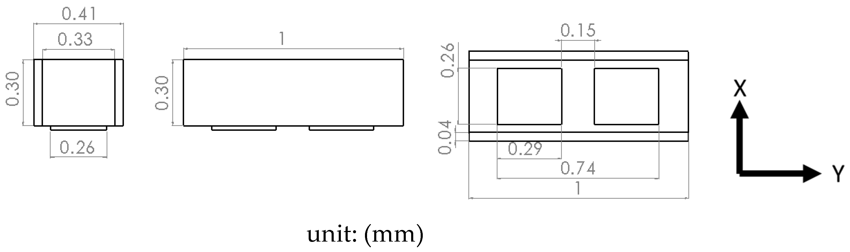
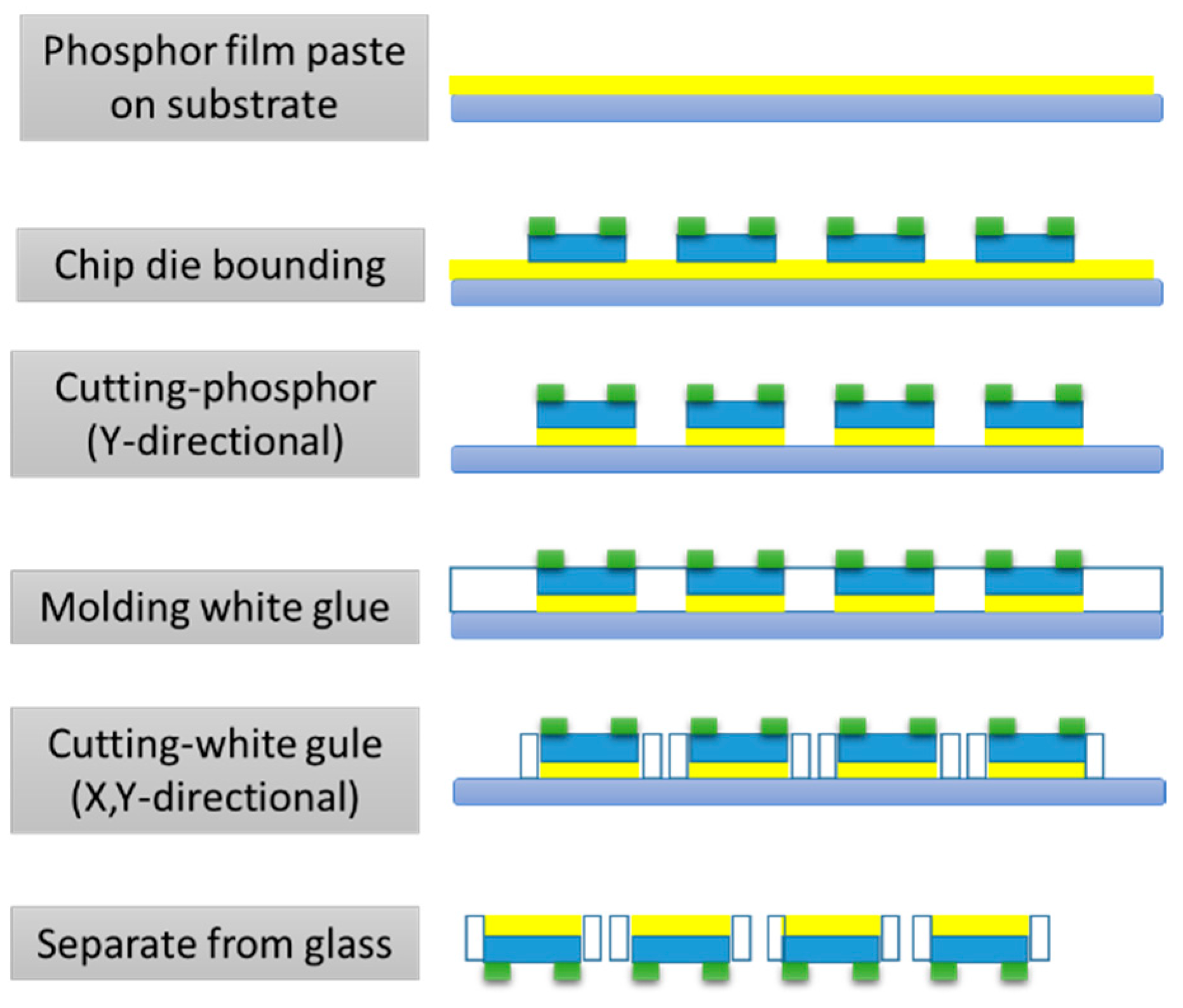
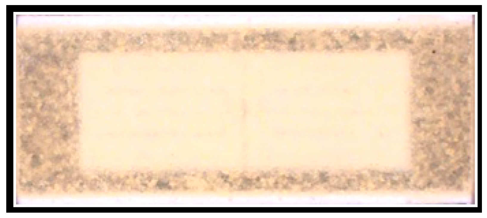
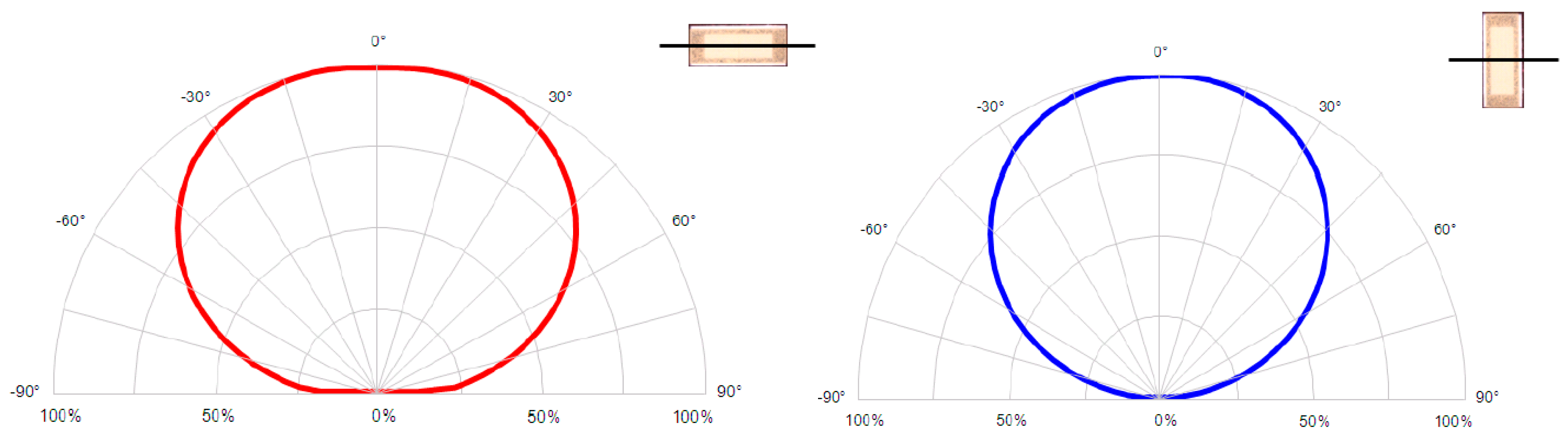
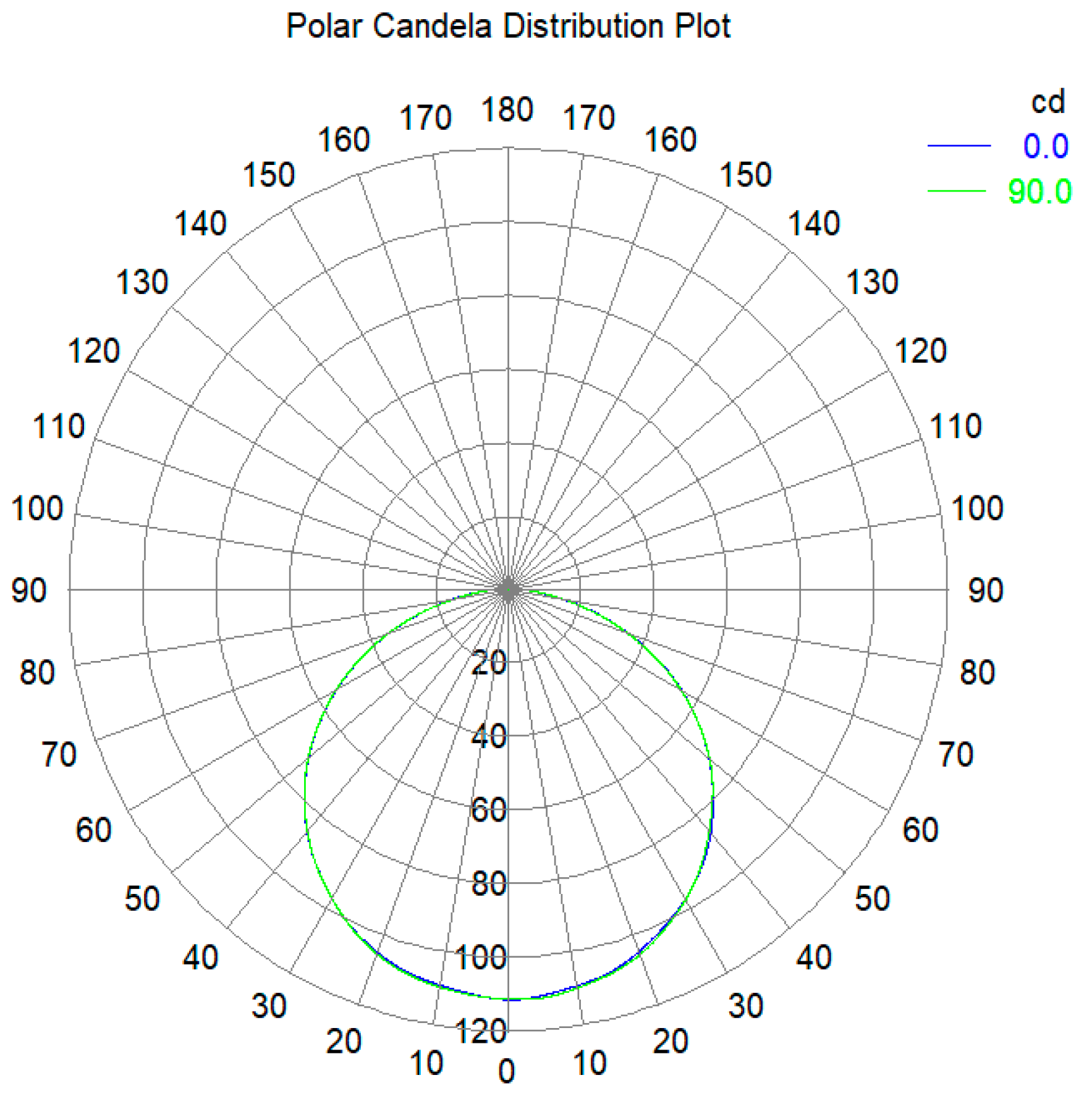
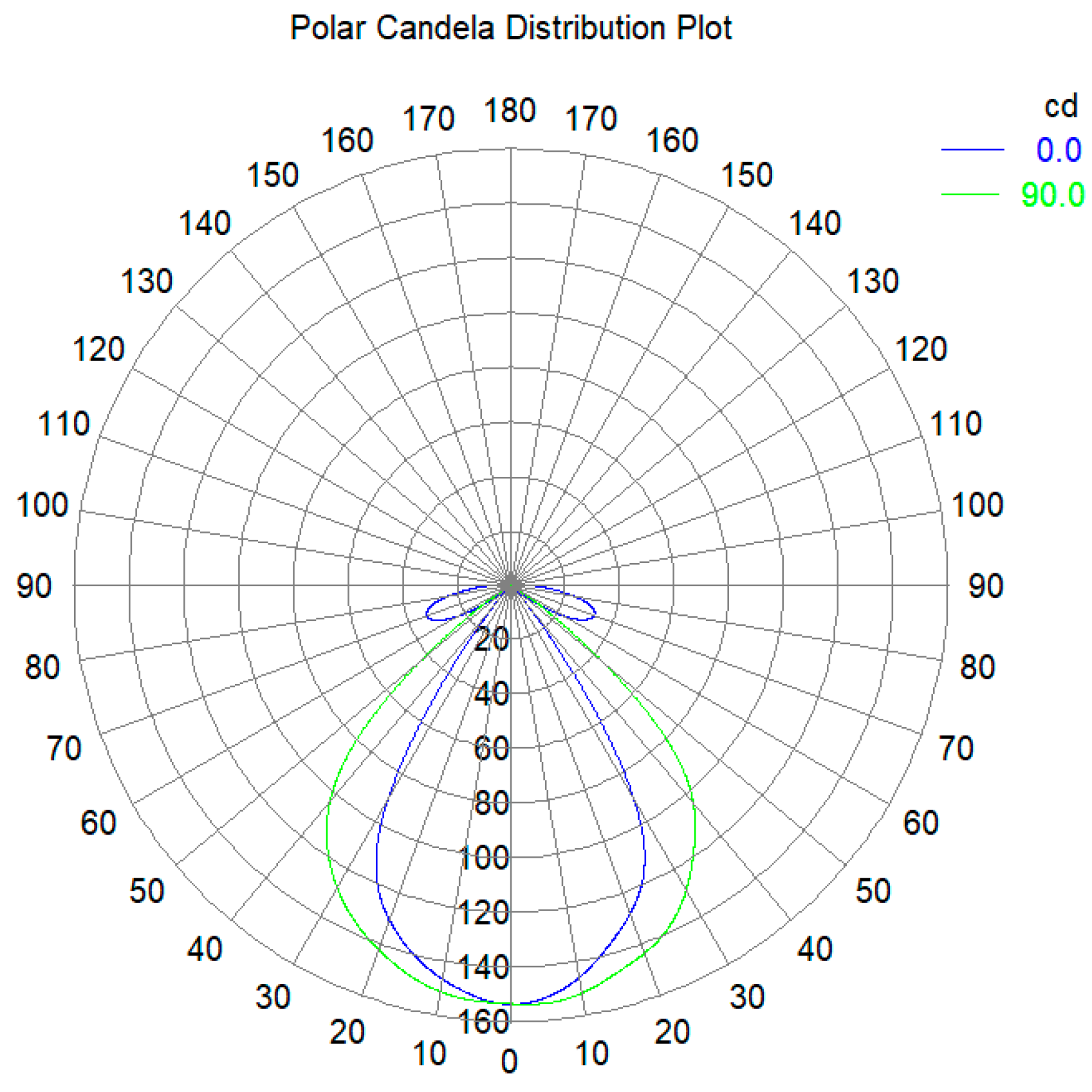
2. Asymmetric Intensity Distribution of Mini-LED Packaging Process

Using flip chips offers many advantages, such as no wire bonding, a lower thermal resistance of packages, the ability to withstand a high current density, and the absence of a lead frame, all of which help in the design of asymmetric intensity distribution (AID) for the packaging process. This study used an AID mini-LED of the flip chip type, employing a chip size of 740 µm × 260 µm × 150 µm. The mini-LED packaged size was 1000 µm × 410 µm, which is illustrated in Figure 1. Figure 2 presents the mini-LED packaging process. The first step of the packaging process involves depositing a phosphor film on a glass substrate. The second step entails arranging the chip and die bonding, followed by cutting along the chip sidewalk. The third step involves applying molding white glue along the long side of the chip, and then cutting along the long side. The final step entails separating the mini-LEDs from the glass substrate by baking or UV curing.
Figure 3 presents the archetype of an AID mini-LEDs; its intensity profile is depicted in Figure 4.
Figure 4 illustrates that the angles relative to the horizontal and vertical axes were 150° and 120°, respectively.

3. Simulation of Light Guide Plate with Asymmetric Intensity Distribution of Mini-LEDs

A traditional backlight includes a light guide plate, reflector film, dot pattern, diffusion film, and prism films, and the dot pattern design is a key factor for obtaining a high efficiency and uniformity, because the dot patterns prevent the total internal reflection. Among these aforementioned elements, dot pattern design is the most time-consuming and resource-heavy work, because the density of the dots must be adjusted several times in order to achieve a uniform light output for the light guide plate. We proposed removing the dot pattern design and replacing it with a fully printed diffusion reflection on the bottom surface of the light guide plate using AID mini-LEDs. The surface property of a dot pattern layer and a fully printed diffusion reflection layer is the Lambertian reflectance.
The proposed light guide plate without dot pattern architecture does not have any of these components or films; instead, it only involves a prism film. Figure 5 presents a comparison of a traditional solid light guide and the proposed fully printed diffusion reflection light guide without dot patterns for use as planar light modules. This design avoids the time required for fabricating the dot pattern design, and is more convenient to use in general lighting.
Table 1 lists the surface and material parameters of all of the components of the light source module used in the simulation.
The uniformity is defined in Equation (1) [19]. Here, the minimum and maximum are the illuminance (E) values that can be measured from the detection surface.
Uniformity = 100 %   minimum   E   ( l u x ) maximum   E   ( l u x )

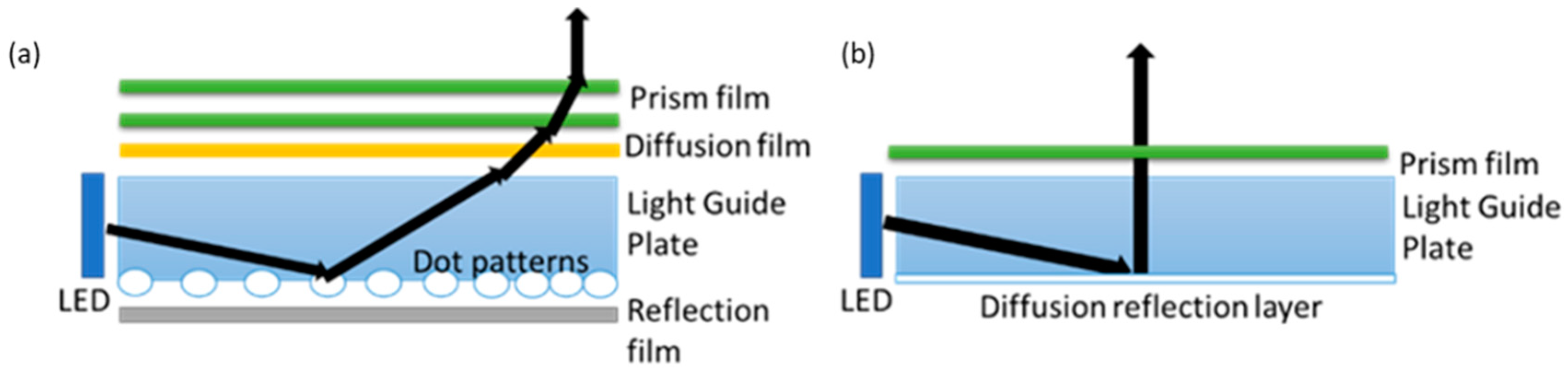
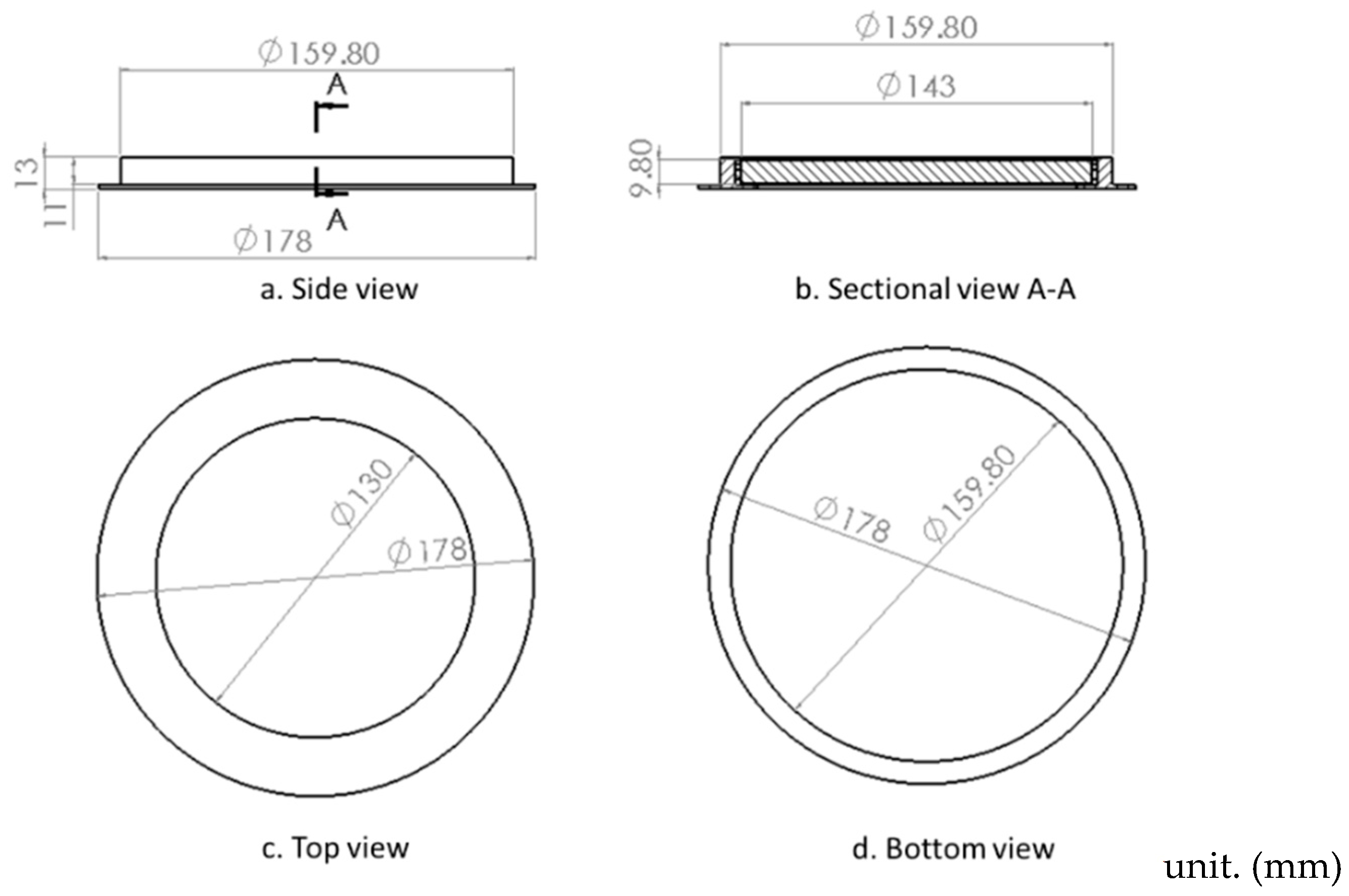
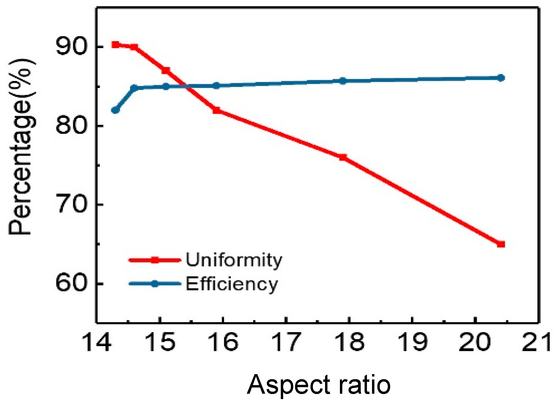
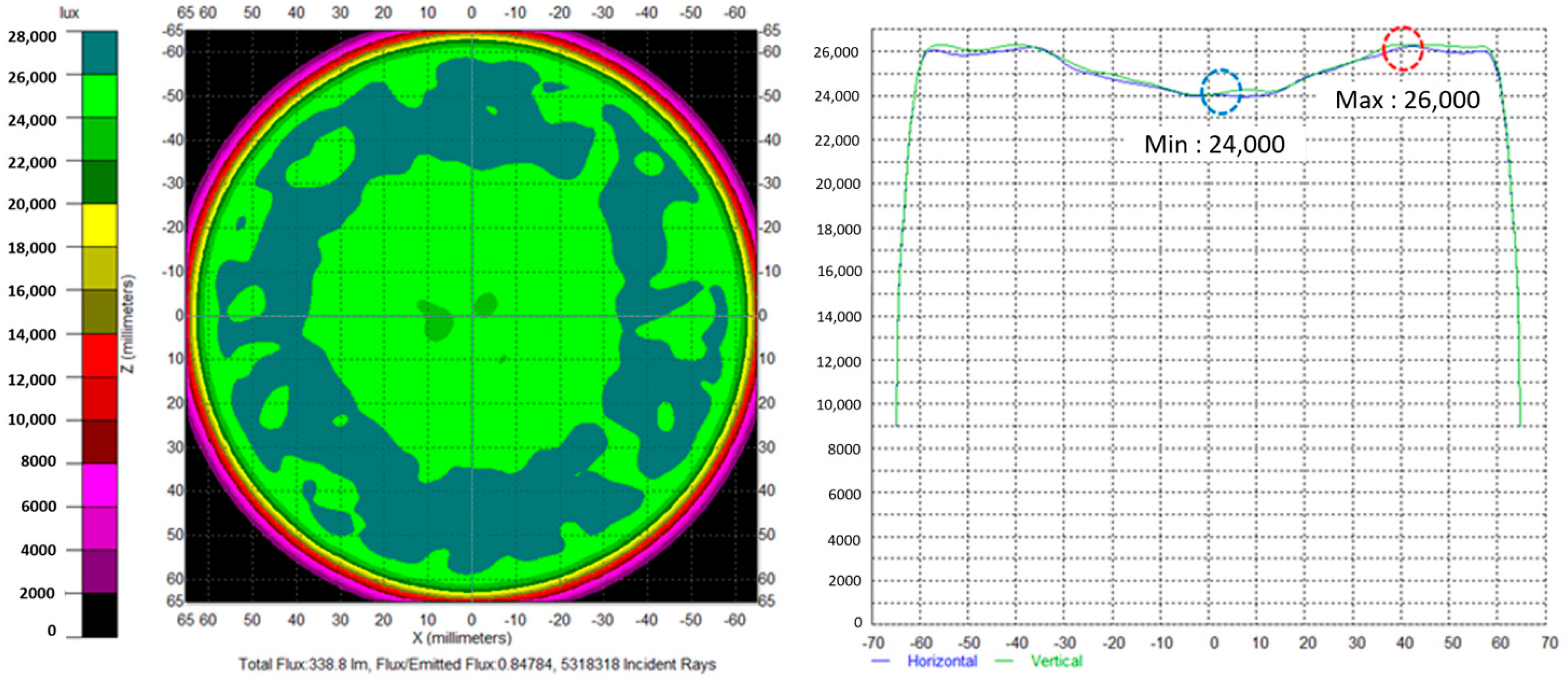
Circular Shape Light Guide Plate with Fully Printed Diffusion Reflection on Bottom Surface
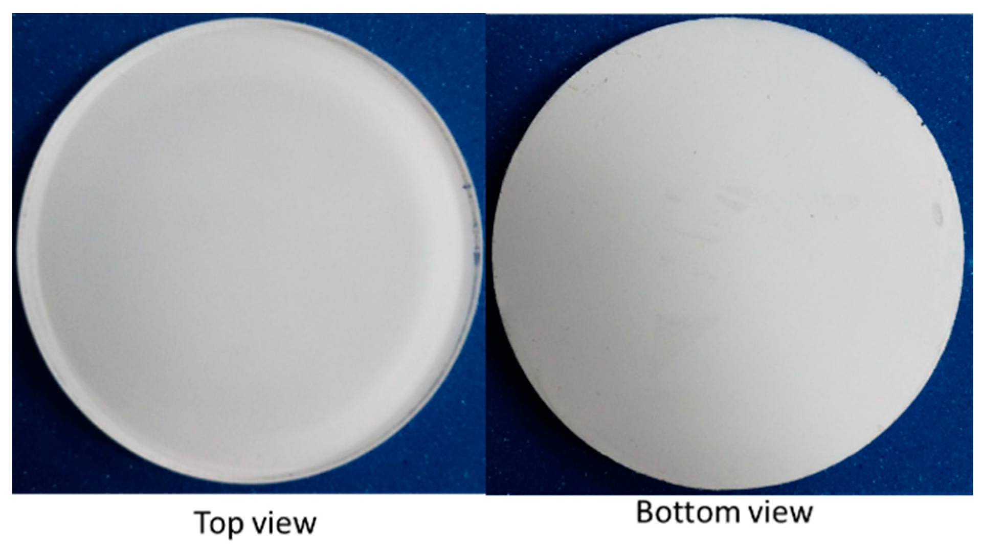
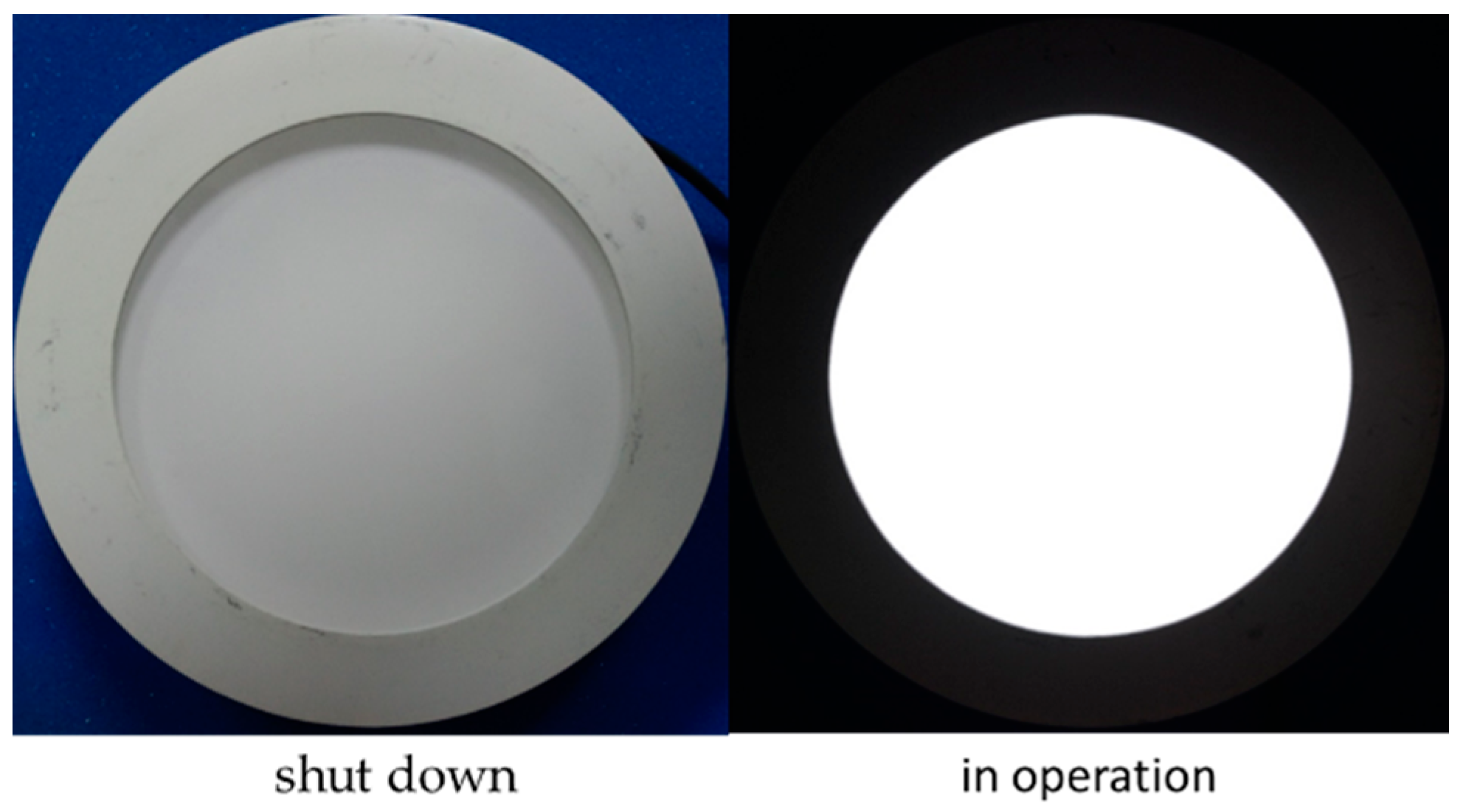
A simulation was conducted to demonstrate the effectiveness of the proposed light guide plate without a dot pattern. Specifically, a ray-tracing simulation was performed using the TracePro (LAMBDA Corp., Littleton, MA, USA). The module containing the proposed light guide plate without a dot pattern had a thickness of 9.8 mm (H0), a length of 143 mm (L0), and a diameter of 143 mm (W0), as depicted, and using an AID mini-LED in 60 pcs, the ring arrangement had the same pitch as in Figure 6.
In our simulation, we set the length (L0) as constant and varied the height in order to evaluate the best ASR (Aspect ratio) of the optical cavity. Table 2 presents the efficiency and uniformity simulated at various ASR values.
Figure 7 illustrates the relationship between efficiency and uniformity at various ASR values. At an ASR value of 14.6, the observed uniformity was superior to the efficiency; nevertheless, the efficiency was still reasonably high.
Figure 8 shows TracePro simulating and using six million rays, and the smoothing properties setting pixels 30 illustrates the illumination map observed for the light guide plate with a fully printed diffusion reflection on the bottom surface, a height of 35 cm, an input of 5 W, and an LED total input of 400 lm. Figure 9 depicts the intensity distribution curve in the detector. The uniformity was 92% and the overall efficiency was 84.8%.
Figure 9 presents the normalize intensity distribution curve in the detector. The horizontal (0°) and vertical (90°) axes were 118°.
Figure 10 illustrates the normalize intensity distribution curve in the detector with one prism film; the horizontal (0°) and vertical (90°) axes were 90° and 62°, respectively.
From the simulation results, we obtained the ASR of a circular shape planar light source where the optimized maximum value was 14.6.

4. Experiment

Figure 11 presents the archetype of the circular shaped light guide plate with a fully printed diffusion reflection on the bottom surface.
Figure 12 presents the illumination map that was observed when the module was shut down and in operation, respectively.
The measured intensity curve without a prism film is depicted in Figure 13, using the approximation simulation data from Figure 9, the intensity curve with one prism film from Figure 14, and the approximation simulation data from Figure 10.
Nine equidistant points were established in order to evaluate the uniformity (depicted in Figure 15), which was obtained using a BM-7 luminance meter (Topcon Corporation, Tokyo, Japan). The uniformity was evaluated in order to determine Lmin/Lmax × 100%. Table 3 lists the measurement results. The relative luminance (L) measured at point 1 was 92.6%.
Table 4 lists the measured data of the optical characteristics. The data in Table 4 was measured using an integrating sphere (Isuzu Optical, Hsinchu, Taiwan); the efficiency was 85% and the CIE 1931 chromaticity was coordinated at x = 0.3203, y = 0.3136.
Table 5 lists the simulation and measurement values, which indicate a high coincidence.

5. Conclusions

A novel planar light source module designed using a light guide plate without a dot pattern was proposed. The designs involved an AID with mini-LEDs and a light guide plate with fully printed diffusion reflection on the bottom surface, in order to achieve high efficiency and uniformity. The prototype demonstrated a uniformity of 92.6% and an efficiency of 85%. The proposed architecture is feasible as a high efficiency and uniformity solution for a six-inch planar illuminator, and is thus more suitable for the downlight in general lighting applications.

Author Contributions

All of the authors have thoroughly discussed the paper and contributed equally to it.

Funding

The authors would like to thank the Ministry of Science and Technology of Taiwan for their financial support under grant number MOST107-2221-E-009-113-MY3.

Conflicts of Interest

The authors declare no conflicts of interest.

References

  1. Yu, J.-C.; Hsu, P.-K. Design optimization and stamper fabrication of light guiding plates using silicon based micro-features. In Proceedings of the 2009 Symposium on Design, Test, Integration & Packaging of MEMS/MOEMS, Rome, Italy, 1–3 April 2009; pp. 202–207. [Google Scholar]
  2. Kang, M.-W.; Guo, K.-X.; Liu, Z.-L.; Zhang, Z.-H.; Wang, R.-Z. Dot pattern designing on light guide plate of backlight module by the method of molecular potential energy. J. Disp. Technol. 2010, 6, 166–169. [Google Scholar] [CrossRef]
  3. Zhao, H.; Fang, S.; Shang, B. Adaptive neuro-fuzzy inference system for generation of diffuser dot patterns in light guides. Appl. Opt. 2010, 49, 2694–2702. [Google Scholar] [CrossRef]
  4. Chen, E.; Lin, Z.; Lin, J.; Guo, T. Design and demonstration of an integrated light-guide plate for LED backlights. In Proceedings of the 2014 International Optical Design Conference, Kohala Coast, HI, USA, 22–26 June 2014. [Google Scholar]
  5. Joo, B.-Y.; Ko, J.-H. Simulation Study of Injection-Molded Light Guide Plates for Improving Luminance Uniformity Based on the Measured Replication Quality of Micro-Patterns for LED TV Backlight. J. Opt. Soc. Korea 2015, 19, 159–164. [Google Scholar] [CrossRef] [Green Version]
  6. Chen, C.-F.; Kuo, S.-H. A highly directional light guide plate based on V-groove microstructure cell. J. Disp. Technol. 2014, 10, 1030–1035. [Google Scholar] [CrossRef]
  7. Fang, Y.-C.; Tzeng, Y.-F.; Wu, K.-Y. A study of integrated optical design and optimization for LED backlight module with prism patterns. J. Disp. Technol. 2014, 10, 812–818. [Google Scholar]
  8. Yan, J.-R.; Wang, Q.-H.; Li, D.-H.; Zhang, J.-D. Edge-lighting light guide plate based on micro-prism for liquid crystal display. J. Disp. Technol. 2009, 5, 355–357. [Google Scholar] [CrossRef]
  9. Xu, P.; Huang, Y.; Su, Z.; Zhang, X.; Luo, T.; Peng, W. Research of micro-prism distribution on the bottom surface of the small-size integrated light guide plate. Opt. Express 2015, 23, 4887–4896. [Google Scholar] [CrossRef] [PubMed]
  10. Zhang, H.; Zhu, J.; Li, Q.; Tan, Q. Design of Light Guide Plate using White Light Emitting Diode for Direct Illumination of Liquid Crystal Display. In Proceedings of the 2010 Symposium on Photonics and Optoelectronics, Chengdu, China, 19–21 June 2010; pp. 1–4. [Google Scholar]
  11. Zhang, R. Directional backlighting system using a light guide with paired microstructures. Appl. Opt. 2017, 56, 6735–6741. [Google Scholar] [CrossRef] [PubMed]
  12. Pan, J.-W.; Fan, C.-W. High luminance hybrid light guide plate for backlight module application. Opt. Express 2011, 19, 20079–20087. [Google Scholar] [CrossRef] [PubMed]
  13. Pan, J.-W.; Hu, Y.-W. Design of a hybrid light guiding plate with high luminance for backlight system application. J. Disp. Technol. 2013, 9, 965–971. [Google Scholar] [CrossRef]
  14. Ye, Z.T.; Kuo, H.-C.; Chen, C.-H. Thin hollow light guide for high-efficiency planar illuminator. Appl. Opt. 2015, 54, E23–E29. [Google Scholar] [CrossRef] [PubMed]
  15. Ye, Y.; Pu, D.; Zhou, Y.; Chen, L. Diffraction characteristics of a submicrometer grating for a light guide plate. Appl. Opt. 2007, 46, 3396–3399. [Google Scholar] [CrossRef] [PubMed]
  16. Teng, T.-C. A novel feasible digital laser-blastering to fabricate a light-guide-plate of high luminance and efficiency for TV application. J. Disp. Technol. 2013, 9, 800–806. [Google Scholar] [CrossRef]
  17. Fennig, E.A.; Schmidt, G.; Moore, D.T. Design of Multilayer Planar Light Guide Concentrators. In Proceedings of the Optics for Solar Energy 2017, Boulder, CO, USA, 6–9 November 2017; p. RW3B. 4. [Google Scholar]
  18. Yang, J.-C.; Huang, C.-C. Using UV roll-to-plate imprint lithography to fabricate light guide plates with microdot patterns. IET Micro Nano Lett. 2012, 7, 244–247. [Google Scholar] [CrossRef]
  19. Light and Lighting—Lighting of Work Places—Part 1: Indoor Work Places; EN 12464-1:2011; Beuth Verlag: Berlin, Germany, 2011.
Figure 1. Two-dimensional view of mini-light-emitting diodes (LEDs) and their dimensions.
Crystals 09 00141 g001
Figure 2. Mini-LEDs’ packaging process.
Crystals 09 00141 g002
Figure 3. Archetype of an asymmetric intensity distribution (AID) mini-LED.
Crystals 09 00141 g003
Figure 4. Intensity profile of mini-LEDs with AID distribution.
Crystals 09 00141 g004
Figure 5. (a) Solid light guide module for backlight applications and (b) proposed fully printed diffusion reflection light guide module without dot patterns for backlight applications.
Crystals 09 00141 g005
Figure 6. Three-dimensional view of AID mini-LEDs and the dimensions of the module for a circular shaped planar light source.
Crystals 09 00141 g006
Figure 7. Relationship between efficiency and uniformity at various ASR (aspect ratio) values for a light guide plate with a fully printed diffusion reflection on the bottom surface.
Crystals 09 00141 g007
Figure 8. Illumination map observed for the light guide plate with a fully printed diffusion reflection on the bottom surface.
Crystals 09 00141 g008
Figure 9. Normalize intensity distribution curve for the light guide plate with a fully printed diffusion reflection on the bottom surface.
Crystals 09 00141 g009
Figure 10. Normalize intensity distribution curve in the detector with one prism film.
Crystals 09 00141 g010
Figure 11. Archetype of the light guide plate with a fully printed diffusion reflection on the bottom surface.
Crystals 09 00141 g011
Figure 12. Illumination map when the model was shut down and in operation.
Crystals 09 00141 g012
Figure 13. The measured polar candela distribution curve with one prism film, and the (a) horizontal (0°) and (b) vertical (90°) axes at 120°.
Crystals 09 00141 g013
Figure 14. The measured polar candela distribution curve with one prism film, and the (a) horizontal (0°) and (b) vertical (90°) axes at 88° and 60°, respectively.
Crystals 09 00141 g014
Figure 15. Measurement points on a light source for uniformity evaluation.
Crystals 09 00141 g015
Table 1. TracePro Simulation setting parameters.
ComponentsSpecifications
Surface CharacteristicsMaterial
Light guide platePolish
Refraction index (n) = 1.59
polycarbonate (PC)
Bottom surface of light guide plate (fully printed diffusion reflection)Diffusion white reflection: R = 94%
BRDF: 0.94,
(BRDF=bidirectional reflectance distribution function)
BRDF g = 0,
BRDF B = 0.1,
BRDF A = 0.329132
BRDF define:
Diffusion type: Lambertian
Thickness (mm): 1.5mm
Transmittance ratio: 0.33
Diffusion type: Lambertian
Manufacturer: Entire Technology Company Limited
PC
Prism filmIndex = 1.59
Surface: polished
Prism Angle (degrees): 90
Prism Pitch (µm): 50
Caliper (µm): 152
Thickness(µm): 155
Model: 3M AEF-155
Manufacturer: (3M; MN, USA)
polyethylene terephthalate
(PET)
Table 2. Simulated efficiency and uniformity with aspect ratio.
Aspect Ratio (ASR = W0/H0)Uniformity (%)Efficiency (%)
20.46586.1
17.97685.7
15.98285.1
15.18785
14.69084.8
14.390.382
Table 3. Relative luminance measured at nine points.
PositionRelative Luminance (L; unit: nits)
P11
P20.976
P30.965
P40.947
P50.926
P60.938
P70.963
P80.971
P90.992
Table 4. Measured data of optical characteristics.
CIE xCIE yFlux (lm)Efficiency (%)
Light source0.32930.3125400100
Light source module 0.32030.313634085
Table 5. Comparison of the simulation and measured data.
ItemSimulation Measured
Uniformity (%)9292.6
Efficiency (%)84.885
Horizontal axis (degree)9088
Vertical axis (degree)6260

