Abstract
We present a phononic crystal to achieve efficient manipulation of surface acoustic waves (SAW). The structure is made of finite phononic micro-ridges arranged periodically in a substrate surface. Each ridge is constructed by staking silicon and tungsten layers so that it behaves as one-dimensional phononic crystal which exhibits band gaps for elastic waves. The band gap allows the existence of resonance modes where the elastic energy is either confined within units in the free end of the ridge or the ones in contact with the substrate. We show that SAW interaction with localized modes in the free surface of the ridge gives rise to sharp attenuation in the SAW transmission, while the modes confined within the ridge/substrate interface cause broad band attenuations of SAW. Furthermore, we demonstrate that the coupling between the two kinds of modes within the band gap gives high SAW transmission amplitude in the form of Fano-like peaks with high quality factor. The structure could provide an interesting solution for accurate SAW control for sensing applications, for instance.
1. Introduction
There have been numerous works and investigations on phononic crystals (PCs), as they provide the solution for acoustic and elastic wave control and dispersion manipulation. PCs are constructed by periodic arrangement of solid materials or fluids, having different elastic properties which allow for the existence of phononic band gaps (BGs) where wave propagation is prohibited [1,2]. This property paved the way for considering PC for many applications such as filtering and waveguiding [3,4,5,6,7,8], sensing [9,10], acoustic wave focusing and lensing [11,12,13,14], and topological phononics [15,16]. The rapid progress in phononics led to the appearance of acoustic metamaterials (AM), which demonstrate exceptional properties such as negative effective mass density, and/or bulk modulus or compressibility [17,18,19,20]. Such behavior led to the creation of new designs for artificial systems, capable of remarkable acoustic wave manipulation such as sound insulation [21], sub-wavelength focusing [22,23], and acoustic cloaking [24].
Among the works on PC and AM, structures based on plates attracted more interest as they offer good platforms for elastic wave propagation and integration, with low loss and weak mode conversion at wavelength larger than the plate thickness. The first PC systems were constructed by considering periodic distribution of holes or inclusions in the plate [25,26]. Then, the phononic community quickly turned their interest to elastic pillars deposited on thin plates, as these showed promising dispersion properties for Lamb waves. Pennec et al. [7,27] and Wu et al. [28,29] proposed a pillar based plate by which they showed the arising of local resonance BG (LRBG) created by the resonances of the pillars which couple with the Lamb waves in the band structure. This behavior was experimentally demonstrated by Wu et al. [28] using a laser ultrasonic technique in an aluminum based pillar plate. In other studies, the acoustic properties of silicone rubber pillars deposited on a rigid plate were investigated [20,30,31]. The structure can produce tunable LRBG at the sonic regime [32], and showed also great performance as a thin sonic insulator with high sound transmission losses [33,34]. Meanwhile, the process of introducing a point or a line defect inside the PC lattice allows for the creation of elastic modes in the BG with zero or slow group velocity. Pennec et al. [7,27] performed elastic waveguiding using a line defect, either by creating a space between two rows of pillars, or by changing the pillars height or their material in a row. In another study, the same group proposed a system with hollow pillars where whispering gallery modes could be used to achieve efficient elastic waveguiding [35]. The modes’ frequency can be tuned by filling the hollow parts with a liquid [36,37]. Wang et al. [38] have shown experimentally similar behavior in a phononic strip. In another study, Wu et al. [29] have demonstrated experimentally the waveguiding feature in a stubbed PC plate using a bent waveguide to change the wave propagation direction in the ultrasonic regime. Very recently, Jin et al. [39] studied the scattering of an incident Lamb wave with a single or a line of pillars, and discussed the amplitudes and phases of monopolar and dipolar waves emitted by these resonators. The Lamb waves confinement and waveguiding were also demonstrated by the pillar based system in the sonic regime [40,41,42].
Motivated by surface acoustic wave (SAW) manipulation in the ultrasonic regime for sensing and filtering applications, some works dealt with the SAW dispersion by PC. The first systems were constructed by tailoring holes or finite inclusions on a substrate surface [5,8,41,42,43,44,45,46]. Later on, interest was turned to PC made of micro-pillars deposited in the surface of a semi-infinite material, for higher dispersion of the SAW. Khelif et al. [47] proposed a two-dimensional array of cylindrical pillars, by which they theoretically demonstrated the BG opening for SAW by local resonance of the pillars. In the band structure, they show that the BG creation results from the coupling between resonance modes and SAW, which occurs below the sound cone. This feature is very interesting compared to PC based on inclusions, since one can avoid the SAW interaction with bulk acoustic waves (BAW) (occurring above the sound line) which inevitably increases the SAW energy leakage into the bulk substrate. The mechanical vibrations of pillars were experimentally demonstrated by Achaoui et al. [48] using optical measurements and the arising of LRBG was evidenced through the SAW transmission decay at the resonance frequency. Other works have also detected experimentally the resonance of the pillars in different pillar based PC [49,50]. Yudistira et al. [51] showed the opening of both Bragg BG and LRBG in a hypersonic PC made of pillars, and very recently, Ash et al. [52] were able to detect high SAW attenuation caused by LRBG using a PC system made of pillars in holes (ring holes). In the very low frequency regime for geophysics application, Brûlé et al. [53] proposed a macro-scale metamaterial capable of modifying the seismic energy. Afterwards, Colombi et al. [54] showed that forests could act as locally resonant metamaterials so that Rayleigh waves experienced strong attenuation when interacting with trees.
Meanwhile, few works have investigated the possibility of SAW waveguiding. Lethawe et al. [55] proposed a pillar-based structure where waveguiding is achieved through a chain of pillars. Very recently, Benchabane et al. [56] demonstrated experimentally the possibility for manipulating the elastic waves in the surface of a substrate using micro-pillars where the elastic energy can be strongly confined at the sub-wavelength scale. For SAW waveguiding achievement by taking advantage of the BG, the classical approach is to introduce a line defect inside the PC to create confined modes within the defect at the BG frequency range. However, this approach makes the defect modes suffer from mode’s conversion and become leaky toward the bulk substrate. In the transmission spectrum, the defect modes have large bandwidth to even close the BG, which makes the system unsuitable for sensing applications, for example.
In this paper, we introduce a PC made of a repetition of phononic ridges built using alternating silicon and tungsten layers (Figure 1 left and Figure 2a). Each ridge is a one-dimensional (1D) PC displaying band gaps where confined modes can be created both in the upper surface of the ridge and its interface with the substrate. We then took advantages of the (1D) PC properties to perform efficient coupling between the SAW and the localized modes in the ridge in order to get high SAW transmission in a very narrow bandwidth. The objective is to get and control high transmitted narrow bands with low radiation into the bulk substrate leading to high QF features. The paper is organized as follows: Section 2 presents the phononic ridge and its dispersion property for elastic waves, and discusses the SAW interaction with the PC made of finite phononic ridges. In Section 3, we study the SAW transmission through one and three ridge(s) and discuss the coupling mechanisms between the modes of interest.
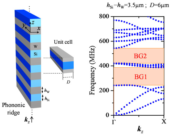
Figure 1.
(Left) Phononic ridge made of periodic repetition of silicon and tungsten layers. (Right) the band structure along kz direction for h = hSi = hW = 3.5 µm and D = 6 µm.
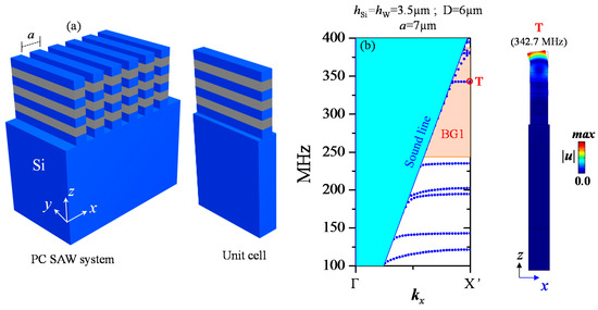
Figure 2.
(a) Phononic crystal (PC) structure made of periodic phononic ridges on Si substrate surface along x direction. (b) Band structure of the PC system for surface acoustic wave (SAW) propagation along x direction. The orange shaded region corresponds to the band gap BG1 of the phononic ridge. (Right) Total displacement field amplitude in the unit cell for mode denoted T in the band structure.
2. SAW Dispersion in the PC System with Phononic Ridges
We first consider an infinite phononic ridge or plate composed of alternating silicon (Si) and tungsten (W) layers (a periodic beam) in z direction, having the same thickness h, while both layers have the same width D (Figure 1). The system is considered infinite along y direction. When choosing h = 3.5 µm and D = 6 µm, the band structure of the system displays two BGs, denoted BG1 from 243.7 to 387.4 MHz and BG2 from 421.3 to 543 MHz, for wave propagation along the z direction (Figure 1). The calculations are based on finite element method using Comsol Multiphysics© software (Comsol, Stockholm, Sweden).
Regarding the SAW dispersion, we built a PC structure using a periodic repetition of finite phononic ridges on the surface of a thick silicon substrate (Figure 2a). Each ridge is made of 3 Si/W cells, ending with a last Si layer on top. The repetition period of the ridges is a = 7 µm (the cell period), and the band structure calculation was performed using a unit cell with periodic boundary conditions (PBC) (Figure 2b). The X’ point indicates the Brillouin zone limit π/a in the propagation direction x for SAW. The blue line corresponds to the Si sound line so that the modes located in the cyan shaded region are BAW or leaky surface modes that can radiate into the bulk silicon substrate. The modes located below the sound line are either confined within the surface of the Si substrate or inside the ridge. Some of the modes appear in the orange shaded region which corresponds to the phononic ridge band gap BG1. The modes located in this region cannot propagate into the Si substrate or in the whole ridge. They can only be confined in specific regions of the ridge, as we will see below. The other SAW branches outside the BG1 correspond to modes where the elastic energy is spread all along the ridges.
From the band structure of Figure 2b, we depicted the presence of one particular flat mode denoted T with zero group velocity at 342.7 MHz inside the BG1 region. We plot in Figure 2b the total displacement field amplitude with the deformation shape of the mode where we could clearly see its local resonance nature. The resonance was confined within the top of the ridge where the maximum of the displacement field amplitude was located, and it quickly decayed along the first top Si/W layers of the ridge, with almost no vibration in the other layers. This behavior was expected since the presence of the stop band BG1 (shaded orange region) of the phononic ridge prohibited propagation along the whole ridge. Furthermore, the mode T displayed flexural like mechanical vibration in the top Si/W layers. We notice that the modes located outside the band gaps BG1 region layers are of less interest in this study, since there are resonance modes where the mechanical vibration is along the whole ridges.
We investigated the phononic ridge behavior when changing its geometry. We considered the finite phononic ridge where we change the thickness of the top Si layer, denoted hT in this study (Figure 3a). In the calculations, we considered a single finite phononic ridge with 3.5 Si/W periods where the bottom Si surface is fixed and the upper surface is kept free. If we choose hT = 5.5 µm for the top Si layer, we can depict three confined modes in the band gap BG1 (Figure 3). We plotted in Figure 3b the total displacement field amplitude of these modes to understand their mechanical vibration. The first one, denoted T1 located at 258 MHz, has the same mechanical behavior as the mode denoted T, depicted in the SAW band structure of Figure 2b, where the top Si/W layers display flexural vibration. The second surface-localized mode, denoted T2 at 337.5 MHz, has a compressional vibrational motion shape in which the top Si/W layers are stretched and compressed along the z direction. The third mode T3 (373.4 MHz) has flexural mechanical vibration like mode T1 and can be considered as second order flexural mode. We display in Figure 3c the frequency dependence on the top Si layer thickness hT for the three surface modes where the black squares indicate the mode T1, while the red dots and blue triangles are for resonance modes T2 and T3 respectively. The band gap BG1 is indicated by the orange shaded region. One can deduce from the result that for each defect mode T1, T2 and T3, the frequency increases when lowering the thickness of the top Si layer. This behavior can be expected, knowing that the cavity modes tend to adapt to the defect size so that their wavelength becomes smaller when decreasing hT.
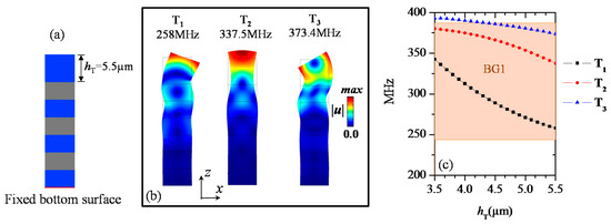
Figure 3.
(a) Finite phononic ridge where the structural defect is constructed by changing the thickness hT of the top Si layer. The bottom surface of the ridge is fixed. (b) Total displacement field amplitude for the resonance modes in the phononic ridge for hT = 5.5 µm. (c) The resonance modes frequency shift as function of hT.
We then investigated SAW dispersion with periodic repetition of finite phononic ridges over the Si substrate surface when changing the top Si layer thickness hT. Figure 4a shows the band structure calculation in the case of hT = 5.5 µm. In the frequency range of the band gap BG1, we can depict three local resonance modes with zero group velocity. We also display in Figure 4b the displacement field amplitude and the deformation profiles of these modes to identify their mechanical behavior. When analyzing the displacement fields, we can clearly identify the flexural resonance modes T1 and T3, and the compressional mode T2, which correspond to the same modes depicted in Figure 3b. Furthermore, the modes T1, T2, and T3 are located at 258, 337.5, and 373.4 MHz, which are at the same frequencies as in the case of isolated ridges presented in Figure 3. We can easily tune the frequency of these localized resonance modes inside the BG1 region by changing the upper Si layer thickness of the ridges.
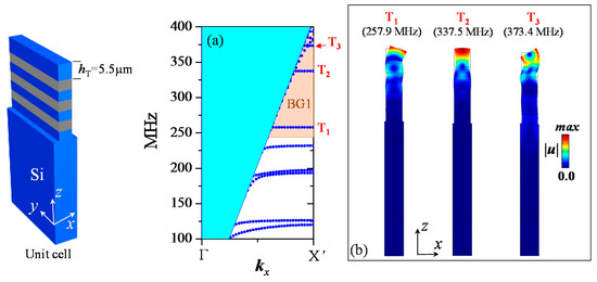
Figure 4.
(a) Band structure for PC system composed of phononic ridges with thickness of the top Si layer hT = 5.5 µm. (b) Total displacement field amplitude |u| for the confined modes inside the band gaps at X’ point.
This time, we considered the case where we also changed the thickness of the Si layer at the bottom of the ridge, denoted hb, in contact with the substrate (Figure 5a). Figure 5b shows the band structures when hb is chosen to be 8 µm, while the top Si layer thickness is hT = 5.5 µm. The other Si and W layers have their thicknesses fixed to 3.5 µm. We also displayed in Figure 5c the total displacement field amplitude |u|, together with the shape of the deformation for the modes inside the band gap BG1 at X’ point. In addition to the presence of the resonance modes T1, T2, and T3 where the mechanical vibration is confined in the top Si/W layers, we observe the appearance of two modes denoted A and B in the band structure inside the BG1 (shaded orange region) (Figure 5b). The displacement field maps of these modes show that they are local resonance modes with almost zero group velocity at the X’ point of the first Brillouin zone. For both modes A and B, we can clearly see that the elastic energy is confined within the bottom Si/W layers close to the substrate surface, with a quickly decaying of the displacement amplitude along the upper Si/W layers and almost no vibration in the top layers of the ridge. Furthermore, when analyzing the mode’s deformation shape, we can clearly see that mode A has flexural-like vibrations of the ridge. The mechanical vibrational motion of mode B is mainly along z direction and corresponds to a compressional-like vibration where the two bottom Si and W layers are stretched and compressed along z direction. Furthermore, one can observe in Figure 5 that the defect modes T1, T2, and T3 are in the same frequencies as in the case of Figure 4 since these modes are not affected by the thickness change of the bottom Si layer.
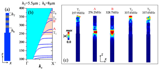
Figure 5.
(a) Unit cell of the PC system where the thickness of the bottom Si layer hb is fixed to 8 µm while the top Si layer thickness is hT = 5.5 µm. (b) Band structures for PC system. (c) Total displacement field amplitude |u| for the confined modes inside the band gaps at X’ point.
We ended up with an interesting feature for this system, which was the existence of two families of cavity modes: one where the elastic energy is confined in the top of the phononic ridge, and the other within the bottom layers in contact with the substrate. We also had the possibility for tuning the frequencies of the two kinds of modes almost independently by either varying the thickness of the upper or bottom Si layers. In the next section, we studied the excitation of these modes by performing SAW transmission calculations, and investigated the coupling between the modes of interest.
3. SAW Transmission through a Phononic Ridge
In this section, we studied the interaction between the SAW and a single phononic ridge by transmission calculations, as schematically described in Figure 6a. Later we shall discuss the effect of a series of parallel ridges. The objective was to understand the coupling mechanisms between the surface modes, the localized modes in the bottom of the ridge, and the SAW inside the BG1 region. We considered the same finite phononic ridge as the one displayed in Figure 4. Figure 6a presents the model constructed for the transmission calculation where Inter-Digital Transducers (IDT) lines footprints were used to excite the SAW at the central frequency 350 MHz of the band gap BG1. The domain width used for the calculation was 820 µm in x direction, and Perfectly Matched Layers (PML) were applied to avoid wave reflections at the boundaries, and to model infinite wave propagation into the bulk substrate. The SAW transmission coefficient was calculated by evaluating the total amplitude of the displacement field along the output point indicated in Figure 6a. Figure 6b,c show the transmission spectra for the cases of top layer thicknesses hT = 5.5 µm and hT = 4.7 µm respectively, while the other layer thicknesses are kept fixed to 3.5 µm. The BG1 region of the phononic ridge is shaded orange. For hT = 5.5 µm, we observed the presence of three dips inside the BG1, located at frequencies 257.9, 337.5, and 373.6 MHz. At these frequencies, we plot in Figure 7 the total displacement field in the phononic ridge, as well as the component in the substrate. To be more specific, the calculation was performed in the frequency domain where each displacement field component could be expressed as:
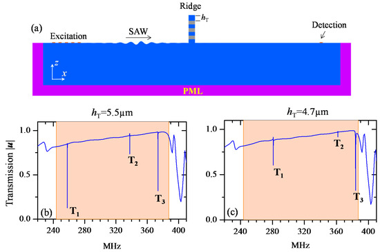
Figure 6.
(a) Schematic view of the model used for the transmission calculation through one phononic ridge. (b,c), Transmission spectra: normalized total displacement’s amplitude for hT = 5.5 µm (b) and hT = 4.7 µm (c). The shaded region indicates the phononic BG of the ridge.
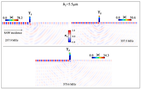
Figure 7.
Total displacement field in the ridge as well as the component in the Si substrate for SAW at the frequencies of the modes T1, T2 and T3 indicated in Figure 6 for hT = 5.5 µm.
For the ridge, we plotted the total displacement field amplitude in each point in the ridge:
We also chose to represent the deformation (with a scale factor for the sake of clarity) for each point of the ridge at the same instant of time chosen for the component plot in the substrate. We clearly saw that the dips originate from the excitation of resonance modes where the mechanical vibration is localized in the top Si/W layers of the ridge. They correspond to the resonance modes T1, T2 and T3 observed in Figure 4 at the same frequencies. The dips are created by the excitation of the resonance modes which couples with Rayleigh waves, causing narrow band transmission loss with part of the elastic energy radiating into the bulk substrate. More precisely, when the SAW hits the ridge, an amount of the elastic energy is transmitted through the ridge inside the BG, as we considered only three cells. The resonance modes would then be excited in the top of the ridge. One can consider the top Si/W layers as a cavity where the elastic energy is stored at the resonance frequency and scattered back along the ridge into the substrate. This mechanism results in SAW dips (loss) in the transmission spectrum in a narrow band corresponding to the resonance modes. Also, it seems that the coupling is stronger for the flexural surface modes T1 and T3 where higher SAW attenuation is depicted, compared to the case of the compressional mode T2. Furthermore, when looking closely to the mechanical vibration amplitudes, we noticed that at the modes resonance frequency, the maximum of the displacement amplitude in the ridge was at least one order of magnitude higher than the amplitude of SAW for the three dips. Additionally, an interesting feature displayed by this system is that we could easily tune the frequencies of the dips only by changing the thickness hT of the top Si layer. When lowering the value of hT from 5.5 to 4.7 µm (Figure 6b,c), the dips frequencies could be increased inside the band gap BG1. The three dips experienced high mechanical QF, which was evaluated at 2.8 × 10⁴, 1.85 × 10⁴ and 7.2 × 10³ for the three modes T1, T2, and T3 respectively in Figure 6c, for instance.
In the following study, we calculated the transmission of SAW through one finite phononic ridge where we changed the thickness of the bottom Si layer of the ridge in contact with the substrate. Figure 8a shows the results where hb is fixed to 8 µm, and the other layer thicknesses are kept equal to 3.5 µm in the ridge. We first observed a large attenuation band (broad dip) in the region of the band gap BG1 where the SAW transmission was around 60% between 293 and 361 MHz. Actually, this decay in the transmission was caused by the SAW excitation of the flexural mode A and the compressional mode B observed in Figure 5, where the mechanical vibration was confined within the bottom Si/W layers of the ridge in contact with the substrate. More precisely, the broad dip in the BG1 resulted from the overlapping of the two wide band dips associated with the modes A and B, as we shall see more clearly when considering the transmission through a series of three ridges. Furthermore, we also noticed the presence of a sharp transmission peak/dip around 342.7 MHz (zoom of the peak/dip in the right panel) in the transmission spectrum. We plot in Figure 9a–c the total displacement field in the ridge and the out-of-plane displacement component in the substrate, respectively at 300 and 356 MHz, as indicated by red arrows in the attenuation band and at the peak frequency 342.7 MHz in Figure 8a. From Figure 9a,b, we observed the excitation of the flexural mode A and the compressional mode B, where the strain energy was confined within the bottom layers of the phononic ridge in contact with the substrate. Also, we easily deduced from Figure 9c that the peak/dip located at 342.7 MHz corresponded to the flexural resonance mode T1 at the surface of the ridge which was at the same frequency as in the case of Figure 2.
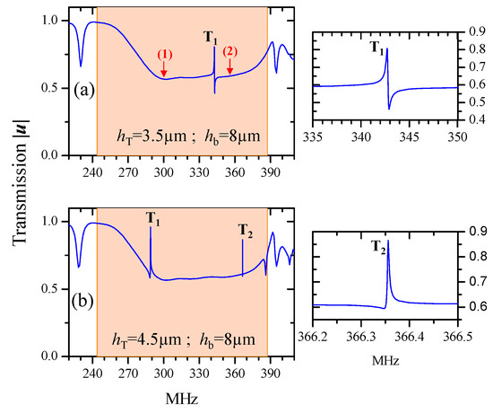
Figure 8.
Transmission spectra: normalized total displacement’s amplitude for hT = 3.5 µm (a) and hT = 4.5 µm (b). The bottom Si layer thickness is fixed to hb = 8 µm. The right panels are zooms of the peaks of interest for each transmission curve.
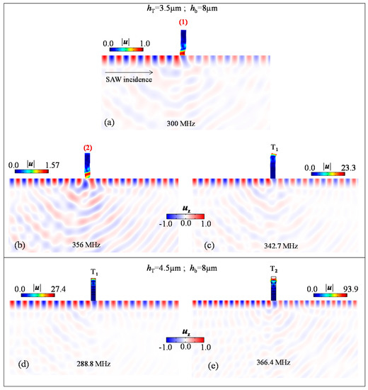
Figure 9.
Total displacement field in the ridge as well as the component in the Si substrate at the frequencies indicated by a red arrows (a), (b) and T1 (c) in Figure 8a for the case of hT = 3.5 µm. The lower panel is for the case hT = 4.5 µm at the frequencies of the peaks T1 (d) and T2 (e) in Figure 8b.
Meanwhile, we plotted in Figure 8b the transmission spectrum for the case where we increased the thickness of the Si top layer hT to 4.5 µm while hb was fixed to 8 µm. We observed the existence of two peaks at 288.8 MHz and 366.4 MHz where we had 96% and 87% of the maximum SAW transmission respectively. When analyzing the displacement field shapes of these two peaks displayed in Figure 9d,e, one can easily conclude that they correspond to the resonance modes T1 and T2, which are excited at their natural frequency, as we could deduce from Figure 3c for the chosen hT = 4.5 µm. From Figure 8, we concluded that upon increasing of the top Si layer thickness hT, the frequencies of modes T1 and T2 decreased so that T2 falls into the BG1 region when hT = 4.5 µm.
In summary, we derived an interesting feature regarding this system. First, the SAW interaction with the ridge resulted in the excitation of localized resonance modes, where the mechanical vibration was confined within the top layers of the ridge, i.e., modes T1, T2, and T3 in Figure 6. These modes fell into the phononic band gap BG1, and their natural frequency could be tuned by changing the thickness of the upper Si layer hT. The SAW interaction with the resonance modes resulted in a quick decay of the SAW amplitude in a very narrow bandwidth, observed as sharp dips in the transmission spectrum (Figure 6b,c). Meanwhile, when introducing a defect in the bottom of the phononic ridge by changing the thickness of the Si layer in contact with the substrate, we could create another kind of mode where the mechanical vibration was confined within the Si/W bottom layers of the ridge, i.e., modes A and B in Figure 5b. The excitation of these modes by SAW resulted in a wider bandwidth attenuation in the transmission. When the frequencies of the resonance modes T1, T2 of the ridge fell into the attenuation band, the transmission curve displayed an asymmetric peak feature (Figure 8b) known as Fano-like resonance [57], in the form of high SAW transmission with a very narrow band. The origin of this Fano-like behavior came from strong coupling between each of the resonance modes T1 and T2, and the confined modes A and B within the band gap region BG1. The Fano resonance was observed experimentally by Nardi et al. [58,59] for SAW in PC, where the resonance resulted from coupling between surface modes and BAW. In our proposed multilayered ridge structure, the origin of the resonances was different; they resulted from the coupling between the surface modes localized on the top free surface of the ridge and the confined modes within the substrate/ridge interface.
Finally, we calculated the SAW transmission over three phononic ridges 21 µm apart to avoid interaction between the ridges. The ridges had their bottom Si layer thickness fixed to hb = 8 µm. In Figure 10, we plotted the transmitted SAW amplitude where the top Si layer thickness hT was chosen to 4.25 µm (a) and 4.9 µm (b) respectively. First, we could distinguish in both transmission curves the existence of two large attenuation bands indicated by A and B which corresponded to the flexural mode and the compressional mode in which the mechanical vibrations were confined within the bottom Si/W layers of the ridges. We can clearly see the overlapping of the resonance bands of modes A and B where the transmission is at 11% and 14% respectively. Meanwhile, in Figure 10a, we chose the thickness hT = 4.25 µm so that the resonance mode T1, which has flexural mechanical motion on the top Si layer, falls exactly at the attenuation region caused by the mode A. The coupling between the two modes results in a high transmission peak of 83% at the T1 mode’s frequency 300 MHz. Both modes had the same mechanical motion nature, i.e., flexural vibration, which explained their strong coupling. The total displacement field amplitude in the ridges and the component in the substrate plotted in the lower panel of Figure 10a, showed the excitation of the resonant mode T1 in the three ridges by the SAW at the peak frequency (300 MHz) along with the transmitted SAW. We also had the same behavior in the attenuation band B by coupling this mode with the resonance mode T2, knowing that they both had the same mechanical motion nature, i.e., compressional vibration. In fact, by choosing Si top layer thickness hT = 4.9 µm, the frequency of the compressional mode T2 could be tuned to fall into the attenuation band B where the coupling between the modes resulted in the creation of the peak T2, as depicted in Figure 10b. At the frequency 356.5 MHz of the peak T2, a maximum transmission of 66% was reached for SAW. When analyzing the total displacement field amplitude in the ridges and the component in the substrate plotted in the lower panel of Figure 10b, we could clearly see the excitation of the resonance mode T2 in the three ridges by the SAW. The QF of mode T1 is about 1200 in the case of hT = 4.25 µm (Figure 10a) while the QF of mode T2 is 2.89 × 10⁴ in the case of hT = 4.9 µm (Figure 10b). Moreover, for the two cases where either the resonance mode T1 falls into the dip band A or mode T2 falls into the band B, we had a situation very close to an acoustic analogue of electromagnetically-induced transparency (EIT) [60,61]. In fact, in plasmonic crystals for instance, the coupling between localized surface states (known as Tamm states) and the defect plasmonic state give an EIT-like behavior [62].
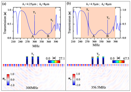
Figure 10.
Transmission results: normalized total displacement’s amplitude for hT = 4.25 µm (a) and hT = 4.9 µm (b). The bottom Si layer thickness is fixed to hb = 8 µm. (Bottom panels) Total displacement field in the ridge as well as the uz component in the Si substrate for SAW at T1 for the case hT = 4.25 µm (a) and T2 for the case hT = 4.9 µm (b).
4. Conclusions
The SAW dispersion over a periodic repetition of periodic multilayered ridges undergoes interesting properties for efficient SAW manipulation. The phononic BG of the ridge allows for the existence of resonance modes localized within the first phononic layers at the free end of the ridge. The SAW interaction with these modes results in a sharp decay of the SAW amplitude in the form of high QF dips. Moreover, another family of confined modes can be created inside the band gap where the elastic energy is confined within the first layers of the ridge in contact with the substrate surface. The excitation of these modes by SAW causes a broad decay of the SAW amplitude in a relatively wide band. The high QF confined modes in the upper free edge of the ridge can couple with the localized modes in ridge/substrate interface to give rise to Fano-like resonance with high QF SAW transmission peaks. This result is a very interesting achievement in the sense that the phononic ridge-based PC can be proposed for efficient manipulation of SAW, with low leakage into the substrate. The structure can introduce a new approach for using PC in SAW based devices to increase the performance of sensing, for instance. Meanwhile, the high transmission peak created by coupling the localized surface modes and the modes confined within the ridge/substrate interface tends towards the arising of an acoustic analogue of EIT. Moreover, a phononic ridge can be used to excite high QF surface phonons, which can then couple with external photons. Very recently, Anguiano et al. [63] and Lamberti et al. [64] demonstrated the confinement of both phonons and photons with strong optomechanic coupling in a composite multilayered GaAs/AlAs micopillar. The composite pillar-based system would be a promising structure for observing quantum optomechanic phenomena, and even for integration into a biosensing platform for instance, to increase device sensitivity. For a practical application in biosensing, the top free surface of the ridge can be functionalized with antigens where specific antibodies can be covalently grafted. The molecular binding event can be monitored through real time observation of the mechanical frequency shift of the localized modes in the SAW spectrum. Moreover, pillared structures have been proposed recently [54] for application in the frame of earthquake damage control by using their resonance frequencies. The behaviors predicted in the multilayered ridge system may pave the way in the macroscale range to new designs of periodically structured ridges so that their transmission spectrum can be tuned to scatter the earthquake surface wave into the bulk. Finally, one can also tailor a defect inside the phononic ridge or pillar to create other cavity modes and achieve the same previous properties to obtain high QF SAW transmission peaks.
Author Contributions
M.O. designed and performed the simulations; B.D.-R. supervised the research; M.O. and B.D.-R. prepared the manuscript; M.O., B.D.-R., Y.P., B.B., and F.S. discussed the results and reviewed the manuscript.
Conflicts of Interest
The authors declare no conflict of interest.
References
- Kushwaha, M.S.; Halevi, P.; Dobrzynski, L.; Djafari-Rouhani, B. Acoustic band structure of periodic elastic composites. Phys. Rev. Lett. 1993, 71, 2022–2025. [Google Scholar] [CrossRef] [PubMed]
- Sigalas, M.; Economou, E.N. Band structure of elastic waves in two dimensional systems. Solid State Commun. 1993, 86, 141–143. [Google Scholar] [CrossRef]
- Kafesaki, M.; Sigalas, M.M.; Garcia, N. Frequency modulation in the transmittivity of wave guides in elastic-wave band-gap materials. Phys. Rev. Lett. 2000, 85, 4044. [Google Scholar] [CrossRef] [PubMed]
- Qiu, C.; Liu, Z.; Mei, J.; Shi, J. Mode-selecting acoustic filter by using resonant tunneling of two-dimensional double phononic crystals. Appl. Phys. Lett. 2005, 87, 104101. [Google Scholar] [CrossRef]
- Wu, T.-T.; Wu, L.-C.; Huang, Z.-G. Frequency band-gap measurement of two-dimensional air/silicon phononic crystals using layered slanted finger interdigital transducers. J. Appl. Phys. 2005, 97, 094916. [Google Scholar] [CrossRef]
- Vasseur, J.O.; Deymier, P.A.; Djafari-Rouhani, B.; Pennec, Y.; Hladky-Hennion, A.-C. Absolute forbidden bands and waveguiding in two-dimensional phononic crystal plates. Phys. Rev. B 2008, 77, 085415. [Google Scholar] [CrossRef]
- Pennec, Y.; Djafari Rouhani, B.; Larabi, H.; Akjouj, A.; Gillet, J.N.; Vasseur, J.O.; Thabet, G. Phonon transport and waveguiding in a phononic crystal made up of cylindrical dots on a thin homogeneous plate. Phys. Rev. B 2009, 80, 144302. [Google Scholar] [CrossRef]
- Sun, J.-H.; Wu, T.-T. Propagation of surface acoustic waves through sharply bent two-dimensional phononic crystal waveguides using a finite-difference time-domain method. Phys. Rev. B 2006, 74, 174305. [Google Scholar] [CrossRef]
- Pennec, Y.; Djafari-Rouhani, B.; Vasseur, J.O.; Khelif, A.; Deymier, P.A. Tunable filtering and demultiplexing in phononic crystals with hollow cylinders. Phys. Rev. E 2004, 69, 046608. [Google Scholar] [CrossRef] [PubMed]
- Amoudache, S.; Moiseyenko, R.; Pennec, Y.; Djafari-Rouhani, B.; Khater, A.; Lucklum, R.; Tigrine, R. Optical and acoustic sensing using Fano-like resonances in dual phononic and photonic crystal plate. J. Appl. Phys. 2016, 119, 114502. [Google Scholar] [CrossRef]
- Wu, T.-T.; Chen, Y.-T.; Sun, J.-H.; Steven Lin, S.-C.; Huang, T.J. Focusing of the lowest antisymmetric Lamb wave in a gradient-index phononic crystal plate. Appl. Phys. Lett. 2011, 98, 171911. [Google Scholar] [CrossRef]
- Zhao, J.; Bonello, B.; Becerra, L.; Boyko, O.; Marchal, R. Focusing of Rayleigh waves with gradient-index phononic crystals. Appl. Phys. Lett. 2016, 108, 221905. [Google Scholar] [CrossRef]
- Zhao, J.; Bonello, B.; Marchal, R.; Boyko, O. Beam path and focusing of flexural Lamb waves within phononic crystal-based acoustic lenses. New J. Phys. 2014, 16, 063031. [Google Scholar] [CrossRef]
- Lin, S.-C.S.; Huang, T.J.; Sun, J.-H.; Wu, T.-T. Gradient-index phononic crystals. Phys. Rev. B 2009, 79, 094302. [Google Scholar] [CrossRef]
- Yang, Z.; Gao, F.; Shi, X.; Lin, X.; Gao, Z.; Chong, Y.; Zhang, B. Topological Acoustics. Phys. Rev. Lett. 2015, 114, 114301. [Google Scholar] [CrossRef] [PubMed]
- He, C.; Ni, X.; Ge, H.; Sun, X.-C.; Chen, Y.-B.; Lu, M.-H.; Liu, X.-P.; Chen, Y.-F. Acoustic topological insulator and robust one-way sound transport. Nat. Phys. 2016, 12, 1124–1129. [Google Scholar] [CrossRef]
- Liu, Z.; Zhang, X.; Mao, Y.; Zhu, Y.Y.; Yang, Z.; Chan, C.T.; Sheng, P. Locally resonant sonic materials. Science 2000, 289, 1734–1736. [Google Scholar] [CrossRef] [PubMed]
- Li, J.; Chan, C.T. Double-negative acoustic metamaterial. Phys. Rev. E 2004, 70, 055602(R). [Google Scholar] [CrossRef] [PubMed]
- Ding, Y.; Liu, Z.; Qiu, C.; Shi, J. Metamaterial with simultaneously negative bulk modulus and mass density. Phys. Rev. Lett. 2007, 99, 093904. [Google Scholar] [CrossRef] [PubMed]
- Oudich, M.; Djafari-Rouhani, B.; Pennec, Y.; Assouar, M.B.; Bonello, B. Negative effective mass density of acoustic metamaterial plate decorated with low frequency resonant pillars. J. Appl. Phys. 2014, 116, 184504. [Google Scholar] [CrossRef]
- Mei, J.; Ma, G.; Yang, M.; Yang, Z.; Wen, W.; Sheng, P. Dark acoustic metamaterials as super absorbers for low-frequency sound. Nat. Commun. 2012, 3, 756. [Google Scholar] [CrossRef] [PubMed]
- Zhou, X.; Assouar, M.B.; Oudich, M. Subwavelength acoustic focusing by surface-wave-resonance enhanced transmission in doubly negative acoustic metamaterials. J. Appl. Phys. 2014, 116, 194501. [Google Scholar] [CrossRef]
- Zhou, X.; Assouar, M.B.; Oudich, M. Acoustic superfocusing by solid phononic crystals. Appl. Phys. Lett. 2014, 105, 233506. [Google Scholar] [CrossRef]
- Farhat, M.; Enoch, S.; Guenneau, S.; Movchan, A.B. Broadband cylindrical acoustic cloak for linear surface waves in a fluid. Phys. Rev. Lett. 2008, 101, 134501. [Google Scholar] [CrossRef] [PubMed]
- Khelif, A.; Aoubiza, B.; Mohammadi, S.; Adibi, A.; Laude, V. Complete band gaps in two-dimensional phononic crystal slabs. Phys. Rev. E 2006, 74, 046610. [Google Scholar] [CrossRef] [PubMed]
- Vasseur, J.O.; Hladky-Hennion, A.-C.; Djafari-Rouhani, B.; Duval, F.; Dubus, B.; Pennec, Y.; Deymier, P.A. Waveguiding in two-dimensional piezoelectric phononic crystal plates. Appl. Phys. Lett. 2007, 101, 114904. [Google Scholar] [CrossRef]
- Pennec, Y.; Djafari-Rouhani, B.; Larabi, H.; Vasseur, J.O.; Hladky-Hennion, A.C. Low-frequency gaps in a phononic crystal constituted of cylindrical dots deposited on a thin homogeneous plate. Phys. Rev. B 2008, 78, 104105. [Google Scholar] [CrossRef]
- Wu, T.-T.; Huang, Z.-G.; Tsai, T.-C.; Wu, T.-C. Evidence of complete band gap and resonances in a plate with periodic stubbed surface. Appl. Phys. Lett. 2008, 93, 111902. [Google Scholar] [CrossRef]
- Wu, T.-C.; Wu, T.-T.; Hsu, J.-C. Waveguiding and frequency selection of Lamb waves in a plate with a periodic stubbed surface. Phys. Rev. B 2009, 79, 104306. [Google Scholar] [CrossRef]
- Oudich, M.; Li, Y.; Assouar, B.M.; Hou, Z. A sonic band gap based on the locally resonant phononic plates with stubs. New J. Phys. 2010, 12, 083049. [Google Scholar] [CrossRef]
- Assouar, M.B.; Oudich, M. Enlargement of a locally resonant sonic band gap by using double-sides stubbed phononic plates. Appl. Phys. Lett. 2012, 100, 123506. [Google Scholar] [CrossRef]
- Oudich, M.; Senesi, M.; Assouar, M.B.; Ruzzene, M.; Sun, J.-H.; Vincent, B.; Hou, Z.; Wu, T.-T. Experimental evidence of locally resonant sonic band gap in two-dimensional phononic stubbed plates. Phys. Rev. B 2011, 84, 165136. [Google Scholar] [CrossRef]
- Oudich, M.; Zhou, X.; Assouar, M.B. General analytical approach for sound transmission loss analysis through a thick metamaterial plate. J. Appl. Phys. 2014, 116, 193509. [Google Scholar] [CrossRef]
- Assouar, B.; Oudich, M.; Zhou, X. Acoustic metamaterials for sound mitigation. C. R. Phys. 2016, 17, 524–532. [Google Scholar] [CrossRef]
- Jin, Y.; Fernez, N.; Pennec, Y.; Bonello, B.; Moiseyenko, R.P.; Hémon, S.; Pan, Y.; Djafari-Rouhani, B. Tunable waveguide and cavity in a phononic crystal plate by controlling whispering-gallery modes in hollow pillars. Phys. Rev. B 2016, 93, 054109. [Google Scholar] [CrossRef]
- Jin, Y.; EI Boudouti, E.H.; Pennec, Y.; Djafari-Rouhani, B. Phononic crystal plate with hollow pillars connected by thin bars. J. Phys. D Appl. Phys. 2017, 50, 425304. [Google Scholar] [CrossRef]
- Jin, Y.; Pennec, Y.; Pan, Y.; Djafari-Rouhani, B. Phononic Crystal Plate with Hollow Pillars Actively Controlled by Fluid Filling. Crystals 2016, 6, 64. [Google Scholar] [CrossRef]
- Wang, T.-T.; Wang, Y.-F.; Wang, Y.-S.; Laude, V. Tunable fluid-filled phononic metastrip. Appl. Phys. Lett. 2017, 111, 041906. [Google Scholar] [CrossRef]
- Jin, Y.; Bonello, B.; Moiseyenko, R.P.; Pennec, Y.; Boyko, O.; Djafari-Rouhani, B. Pillar-type acoustic metasurface. Phys. Rev. B 2017, 96, 104311. [Google Scholar] [CrossRef]
- Assouar, M.B.; Senesi, M.; Oudich, M.; Ruzzene, M.; Hou, Z. Broadband plate-type acoustic metamaterial for low-frequency sound attenuation. Appl. Phys. Lett. 2012, 101, 173505. [Google Scholar] [CrossRef]
- Celli, P.; Gonella, S. Manipulating waves with LEGO® bricks: A versatile experimental platform for metamaterial architectures. Appl. Phys. Lett 2015, 107, 081901. [Google Scholar] [CrossRef]
- Oudich, M.; Li, Y. Tunable sub-wavelength acoustic energy harvesting with a metamaterial plate. J. Phys. D Appl. Phys. 2017, 50, 315104. [Google Scholar] [CrossRef]
- Wu, T.T.; Huang, Z.G.; Lin, S. Surface and bulk acoustic waves in two-dimensional phononic crystal consisting of materials with general anisotropy. Phys. Rev. B 2004, 69, 094301. [Google Scholar] [CrossRef]
- Laude, V.; Wilm, M.; Benchabane, S.; Khelif, A. Full band gap for surface acoustic waves in a piezoelectric phononic crystal. Phys. Rev. E 2005, 71, 036607. [Google Scholar] [CrossRef] [PubMed]
- Benchabane, S.; Gaiffe, O.; Ulliac, G.; Salut, R.; Achaoui, Y.; Laude, V. Observation of surface-guided waves in holey hypersonic phononic crystal. Appl. Phys. Lett. 2011, 98, 171908. [Google Scholar] [CrossRef]
- Yudistira, D.; Pennec, Y.; Djafari Rouhani, B.; Dupont, S.; Laude, V. Non-radiative complete surface acoustic wave bandgap for finite-depth holey phononic crystal in lithium niobate. Appl. Phys. Lett. 2012, 100, 061912. [Google Scholar] [CrossRef]
- Khelif, A.; Achaoui, Y.; Benchabane, S.; Laude, V.; Aoubiza, B. Locally resonant surface acoustic wave band gaps in a two-dimensional phononic crystal of pillars on a surface. Phys. Rev. B 2010, 81, 214303. [Google Scholar] [CrossRef]
- Achaoui, Y.; Khelif, A.; Benchabane, S.; Robert, L.; Laude, V. Experimental observation of locally-resonant and Bragg band gaps for surface guided waves in a phononic crystal of pillars. Phys. Rev. B 2011, 83, 104201. [Google Scholar] [CrossRef]
- Robillard, J.F.; Devos, A.; Roch-Jeune, I. Time-resolved vibrations of two-dimensional hypersonic phononic crystals. Phys. Rev. B 2007, 76, 092301. [Google Scholar] [CrossRef]
- Giannetti, C.; Revaz, B.; Banfi, F.; Montagnese, M.; Ferrini, G.; Cilento, F.; Maccalli, S.; Vavassori, P.; Oliviero, G.; Bontempi, E.; et al. Thermomechanical behavior of surface acoustic waves in ordered arrays of nanodisks studied by near-infrared pump-probe diffraction experiments. Phys. Rev. B 2007, 76, 125413. [Google Scholar] [CrossRef]
- Yudistira, D.; Boes, A.; Graczykowski, B.; Alzina, F.; Yeo, L.Y.; Sotomayor Torres, C.M.; Mitchell, A. Nanoscale pillar hypersonic surface phononic crystals. Phys. Rev. B 2016, 94, 094304. [Google Scholar] [CrossRef]
- Ash, B.J.; Worsfold, S.R.; Vukusic, P.; Nash, G.R. A highly attenuating and frequency tailorable annular hole phononic crystal for surface acoustic waves. Nat. Commun. 2017, 8, 174. [Google Scholar] [CrossRef] [PubMed]
- Brûlé, S.; Javelaud, E.H.; Enoch, S.; Guenneau, S. Experiments on Seismic Metamaterials: Molding Surface Waves. Phys. Rev. Lett. 2014, 112, 133901. [Google Scholar] [CrossRef] [PubMed]
- Colombi, A.; Roux, P.; Guenneau, S.; Gueguen, P.; Craster, R.V. Forests as a natural seismic metamaterial: Rayleigh wave bandgaps induced by local resonances. Sci. Rep. 2016, 6, 19238. [Google Scholar] [CrossRef] [PubMed]
- Al Lethawe, M.; Addouche, M.; Benchabane, S.; Laude, V.; Khelif, A. Guidance of surface elastic waves along a linear chain of pillars. AIP Adv. 2016, 6, 121708. [Google Scholar] [CrossRef]
- Benchabane, S.; Salut, R.; Gaiffe, O.; Soumann, V.; Addouche, M.; Laude, V.; Khelif, A. Sarah Benchabane, Roland Salut, Olivier Gaiffe, Valérie Soumann, Mahmoud Addouche, Vincent Laude, and Abdelkrim Khelif. Phys. Rev. Appl. 2017, 8, 034016. [Google Scholar] [CrossRef]
- Fano, U. Effects of Configuration Interaction on Intensities and Phase Shifts. Phys. Rev. 1961, 124, 1866. [Google Scholar] [CrossRef]
- Nardi, D.; Travagliati, M.; Siemens, M.E.; Li, Q.; Murnane, M.M.; Kapteyn, H.C.; Ferrini, G.; Parmigiani, F.; Banfi, F. Probing Thermomechanics at the Nanoscale: Impulsively Excited Pseudosurface Acoustic Waves in Hypersonic Phononic Crystals. Nano Lett. 2011, 11, 4126–4133. [Google Scholar] [CrossRef] [PubMed]
- Nardi, D.; Travagliati, M.; Murnane, M.M.; Kapteyn, H.C.; Ferrini, G.; Giannetti, C.; Banfi, F. Impulsively Excited Surface Phononic Crystals: A Route Toward Novel Sensing Schemes. IEEE Sens. J. 2015, 15, 5142–5150. [Google Scholar] [CrossRef]
- Boller, K.-J.; Imamoglu, A.; Harris, S.E. Observation of electromagnetically induced transparency. Phys. Rev. Lett. 1991, 66, 2593–2596. [Google Scholar] [CrossRef] [PubMed]
- Fleischhauer, M.; Imamoglu, A.; Marangos, J.P. Electromagnetically induced transparency: Optics in coherent media. Rev. Mod. Phys. 2005, 77, 633–673. [Google Scholar] [CrossRef]
- Dyer, G.C.; Aizin, G.R.; Allen, S.J.; Grine, A.D.; Bethke, D.; Reno, J.L.; Shaner, E.A. Induced transparency by coupling of Tamm and defect states in tunable terahertz plasmonic crystals. Nat. Photonics 2013, 7, 925–930. [Google Scholar] [CrossRef]
- Anguiano, S.; Bruchhausen, A.E.; Jusserand, B.; Favero, I.; Lamberti, F.R.; Lanco, L.; Sagnes, I.; Lemaître, A.; Lanzillotti-Kimura, N.D.; Senellart, P.; et al. Micropillar Resonators for Optomechanics in the Extremely High 19–95-GHz Frequency Range. Phys. Rev. Lett. 2017, 118, 263901. [Google Scholar] [CrossRef] [PubMed]
- Lamberti, F.R.; Yao, Q.; Lanco, L.; Nguyen, D.T.; Esmann, M.; Fainstein, A.; Sesin, P.; Anguiano, S.; Villafañe, V.; Bruchhausen, A.; et al. Optomechanical properties of GaAs/AlAs micropillar resonators operating in the 18 GHz range. Opt. Express 2017, 25, 24437. [Google Scholar] [CrossRef] [PubMed]


© 2017 by the authors. Licensee MDPI, Basel, Switzerland. This article is an open access article distributed under the terms and conditions of the Creative Commons Attribution (CC BY) license (http://creativecommons.org/licenses/by/4.0/).