Abstract
This systematic review presents a critical analysis of multifunctional nanowire sensors, with explicit selection criteria for included studies: we focus on peer-reviewed research, prioritizing studies on semiconductor (ZnO, TiO2, Si), metal (Ag, Au), and carbon-based (CNT) nanowires that report structural innovations, performance breakthroughs, or industrial scalability. We systematically analyze their structural characteristics, advanced fabrication techniques (hydrothermal synthesis, magnetron sputtering, PECVD), and application performance across biosensing, pressure sensing, and gas monitoring. Unlike existing reviews limited to single material classes or application scenarios, this work advances the field by integrating three novel perspectives: it delivers a cross-material comparison of nanowire structure–performance relationships, incorporates an analysis of fabrication strategy scalability for industrial translation, and synthesizes unresolved challenges and future directions. Nanowire sensors exhibit superior sensitivity, rapid response, and broad detection ranges compared to conventional sensors, with significant potential to advance healthcare, environmental monitoring, and flexible electronics.
1. Introduction
In gas sensing applications, semiconductor metal oxides (SMOs) have emerged as the preferred materials due to their high surface-to-volume ratio and exceptional stability. Research on hydrogen sulfide (H2S) detection demonstrates that structurally optimized sensors, such as strategically engineered silicon micropillar arrays, can provide superior growth environments for TiO2 and ZnO nanowires, thereby significantly enhancing gas sensing performance. The fundamental advantages of these nanowire sensors originate from their distinctive structural characteristics: compared to conventional sensors, nanowires exhibit not only extremely high surface-to-volume ratios but also unique electron transport behaviors. For instance, silicon nanowire (SiNW) sensors leverage their nanoscale dimensions to enable a “whole-volume response” mechanism, where molecular binding events induce substantial changes in charge carrier concentration throughout the entire nanowire volume, consequently achieving detection sensitivity far surpassing conventional devices. Furthermore, innovations in material systems continue to expand the application boundaries of sensing technologies. Silver nanowire (AgNW) networks have become ideal candidates for flexible strain sensors owing to their high electrical conductivity and outstanding mechanical flexibility, while silicon-on-insulator (SOI)-like structures have significantly improved both insulation properties and integration density through optimized device design.
To address the need for a structured overview of this rapidly evolving field, this review adopts explicit selection criteria for included studies: we focus on high-impact peer-reviewed research, prioritizing studies on semiconductor (ZnO, TiO2, Si), metal (Ag, Au), and carbon-based (CNT) nanowires that report structural innovations, performance breakthroughs or industrial scalability. Conversely, we exclude studies that lack clear structural characterization or fail to provide comparative performance data against state-of-the-art devices.
This review systematically compares the performance characteristics of nanowire-based sensors and their conventional counterparts, providing an in-depth analysis of their respective advantages and limitations across different application scenarios. By focusing on the structural properties of nanowires, we thoroughly explore their application potential in both gas detection and biosensing, offering valuable insights for the advancement of sensing technologies. With continuous progress in nanotechnology, nanowire-based sensing platforms are expected to enable groundbreaking innovations across multiple domains.
2. Growth, Integration Strategies, and Structural-Property Relationships of Multifunctional Nanowire Sensors
With the continuous advancement of technology, structural sensors have become increasingly important in fields such as engineering, environmental monitoring, and biomedicine. Traditional structural sensors, based on mature materials and technologies, offer significant advantages in terms of cost-effectiveness, durability, and ease of use. The structure of the traditional sensor is shown in Figure 1a, which consists of a substrate, a signal transmission layer, a protective coating layer, and a tapered sensing layer. However, the rise of nanotechnology has brought nanowire sensors to the forefront, with their excellent performance in sensitivity, size, and response time introducing new breakthroughs in structural monitoring. The structure of the nanowire sensor is shown in Figure 1b, which consists of a substrate, a signal transmission layer, a protective coating layer and a nanowire-structured sensing layer.
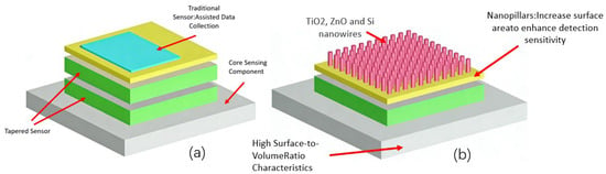
Figure 1.
Schematic diagram of the sensor structures: (a) conventional sensor; (b) nanowire-structured sensor.
The performance differences between the two types of sensors are particularly evident in specific applications such as gas detection. In the field of industrial safety, gas sensors play a critical role in preventing major workplace accidents. Taking hydrogen sulfide (H2S) gas as an example, this highly toxic hazardous substance has attracted widespread attention. According to the U.S. Occupational Safety and Health Administration (OSHA), the permissible exposure limit (PEL) for H2S gas is 50 ppm [1]. Exposure concentrations exceeding this threshold can lead to a range of severe physiological reactions, including impaired motor coordination, memory loss, dizziness, nausea, and loss of smell [2]. In this field, SMOs have become the preferred sensing materials due to their excellent cost-effectiveness, high specific surface area, outstanding detection efficiency, low detection limits, high sensitivity, and good stability [3,4,5,6,7]. Among them, tin dioxide (SnO2) is widely used for H2S gas detection due to its broad concentration response characteristics, excellent selectivity, and reliability in practical applications. It should be noted that although researchers have developed sensing materials with unique nanostructures through various synthesis processes to optimize performance [8,9,10,11,12], most sensing systems based on traditional SMOs still need to operate at relatively high temperatures, which constitutes a major limitation.
To overcome the above limitations, nanowire sensors provide a new approach through structural design. Their performance advantages stem not only from the material itself but also from precise nanostructural design. For example, when comparing two silicon micropillars of different sizes, significant structural differences can be observed between those with an average diameter of 600 nm and a height of 3.2 μm and those with an average diameter of 400 nm and a height of 1.5 μm [13]. Specifically, the larger spacing between adjacent micropillars in the former provides more space for the growth of TiO2 and ZnO nanowires, enabling the nanowires to achieve larger diameters and better crystallinity during the growth process, ultimately leading to better performance in gas sensor applications [13]. This ability to optimize structure and performance at the nanoscale is key to achieving high sensitivity, fast response, and even lower operating temperatures in nanowire sensors. In addition to H2S gas detection, both types of sensors are also widely used in the detection of alcohol molecules, biomarkers, glucose, and other related sensing applications. This paper aims to compare and analyze nanowire sensors and traditional material-based structural sensors, exploring their core advantages and disadvantages in different application scenarios to provide useful references for future sensor selection and application.
In terms of sensor structural integration, substrate and packaging technologies are also crucial. For instance, depositing 145 nm SiO2 and 40 nm polysilicon on a silicon substrate forms a structure similar to SOI [14], offering advantages such as enhanced insulation performance, electrical properties, thermal stability, radiation resistance, electrochemical stability, integration capability, and scalability. This structure effectively isolates charge carriers on the silicon substrate, reduces leakage current, and improves the insulation performance of the device. Meanwhile, the polysilicon layer provides good electrical properties. Due to the isolation effect of the insulating layer, the SOI structure can reduce the impact of radiation on the silicon substrate, enhancing the device’s radiation resistance. Additionally, the SOI structure can mitigate the effects of electrochemical reactions on the silicon substrate, improving the device’s electrochemical stability. This structure facilitates easier integration and packaging of devices, enhances integration density, and allows for more straightforward scalability design, further improving the device’s scalability.
Beyond rigid sensors, nanowires also demonstrate outstanding performance in the field of flexible sensing. The conductive layer formed by AgNWs networks on flexible substrates, characterized by high conductivity, sensitivity, tunable resistance, good mechanical properties, ease of integration, cost-effectiveness, and environmental friendliness, makes them one of the important materials for preparing high-performance strain sensors [15]. This network structure provides more contact points through its cross-linked architecture, increasing the number of conductive paths and thereby enhancing sensor sensitivity. Furthermore, by adjusting the density and arrangement of the AgNWs network, the sensor’s resistance can be tuned to meet the requirements of different applications. The AgNWs network layer exhibits good flexibility and stretchability, allowing it to adapt to various deformations and stresses, ensuring stable sensor performance even in complex environments. At the same time, the AgNWs network layer can be integrated with other materials or structures, such as CNTs and conductive polymers, to enable the construction of multifunctional sensors. The preparation process of AgNWs is relatively simple and low-cost, giving AgNWs-based network layers a high cost-performance ratio in the sensor field. Moreover, AgNWs possess good biocompatibility, allowing them to be safely used in the human body without causing immune reactions or toxic effects [16].
From an overall structural perspective, significant differences exist between traditional sensors and nanowire-based sensors in terms of structure and performance. Traditional sensors are typically based on thin films, film-ceramic composites, or mechanical structures. These sensors have relatively simple structures, primarily composed of a single material or a combination of a few materials. For example, resistive sensors may be based on thin-film resistive materials, while capacitive sensors may rely on thin-film capacitive materials. A sensing concept based on field-effect transistors (FETs) was proposed decades ago and applied to planar FET devices (known as CHEMFETs) [17,18]. However, due to the limited sensitivity of such planar devices, they have not had as profound an impact as chemical or biological sensors. The structures of these sensors are relatively fixed and lack high specific surface area and unique electronic properties.
In contrast, nanowire-based sensors utilize nanowires, such as carbon nanotubes, metal nanowires (e.g., AgNWs, CuNWs), and semiconductor nanowires (e.g., ZnO nanowires, TiO2 nanowires), which possess high specific surface area and unique electronic characteristics [19,20,21]. This structure endows nanowire sensors with higher sensitivity and faster response speeds. For example, silicon nanowire (SiNW) sensors, due to their unique nanostructure and nanoscale cross-section and the ability to be precisely tuned as p-type or n-type materials, exhibit well-defined and reproducible high-performance FET characteristics, significantly overcoming the sensitivity limitations of traditional planar CHEMFETs [22,23,24,25]. Unlike planar devices, which sense only through the surface region, the nanoscale dimensions of SiNWs enable the binding of target molecules to their surface to induce depletion or accumulation of charge carriers throughout the entire volume of the nanowire [26,27,28,29]. This whole-volume response characteristic gives SiNW sensors extremely high detection sensitivity, even enabling detection at the single-particle level [30]. Theoretically, this nanowire-based sensing mechanism is universal; any semiconductor nanowire material can be designed into an FET structure for highly sensitive detection of various biological and chemical substances.
However, nanowire sensors also face several challenges. Controlling the diameter, orientation, and position of nanowires remains challenging in mass production. Certain nanowires (e.g., CuNWs are prone to oxidation, and ZnO nanowires are sensitive to humidity) may experience performance degradation in practical environments, necessitating strategies such as coating (e.g., with SiO2 layers) or material modification to enhance stability [25,26]. With the advancement of nanotechnology, nanowire-based sensors are expected to find applications and development in more fields.
3. Sensing Mechanisms of Nanowire-Based Sensors
3.1. Hydrothermal Reduction Method
The hydrothermal reduction method is a chemical synthesis technique that directly reduces metal ions into metallic nanomaterials within a high-temperature, high-pressure aqueous environment by introducing reducing agents. This technology offers mild reaction conditions, controllable processes, and environmental friendliness, leading to its widespread application in fields such as catalysis, sensors, and electronics. Furthermore, the hydrothermal reduction method enables the one-step synthesis of metallic nanomaterials, eliminating intermediate steps and enhancing synthesis efficiency, making it extensively utilized in materials science and nanotechnology [27].
Directional growth occurring in high-temperature and high-pressure aqueous systems, a technique whose nanowire dimensions are regulated by precursor concentration, is characterized by distinct performance trade-offs: it is a method that boasts low equipment cost and exhibits good compatibility with both metal and semiconductor nanowires [31]; however, it is also a process that suffers from relatively poor batch uniformity and involves relatively long reaction cycles [32,33]. In terms of scalability, this is a technique that is feasible for mass production through continuous-flow reactors and which is well-suited for fabricating heterojunctions in gas sensors [34].
3.2. Radio Frequency (RF) Magnetron Sputtering
Radio frequency (RF) magnetron sputtering technology, as an efficient thin film deposition method, plays a crucial role in modern industry. It utilizes plasma generated by an RF power supply to excite a high-energy ion beam [28]. This ion beam subsequently bombards a target material, sputtering material from the target surface, which is then deposited onto a substrate material to form a thin film. This sputtering process enables the formation of uniform, high-quality films on substrates, characterized by a high deposition rate and strong controllability. Consequently, RF magnetron sputtering finds extensive application in various fields, including semiconductor manufacturing, flat-panel display technology, solar cells, and optical coatings.
RF magnetron sputtering—a physical vapor deposition technique that relies on plasma-induced target sputtering to deposit seed layers on substrates—is frequently integrated with hydrothermal synthesis to fabricate heterojunction nanowires for advanced sensing applications. This technique boasts distinct advantages: it delivers high film uniformity, whose consistency minimizes performance deviations between individual devices and ensures the reproducibility of subsequent nanowire growth; it also enables precise control over seed layer thickness, which lays a robust, homogeneous foundation for directional nanowire nucleation [29]. However, it carries inherent limitations: it is a method that requires substantial investment in specialized equipment, which restricts its accessibility for small-scale research teams; it is a process that depends on stringent high-vacuum environments, which adds complexity and operational costs to large-scale production setups; and it is a technique that faces constraints in tuning nanowire aspect ratios, which limits its adaptability to applications demanding extreme morphological precision. In terms of scalability, this is a method that exhibits moderate potential, as it can be adapted for roll-to-roll processing that caters to flexible substrate fabrication—an attribute that makes it a suitable choice for manufacturing thin-film substrates used in flexible optoelectronic sensors [30].
3.3. Plasma-Enhanced Chemical Vapor Deposition
Plasma-Enhanced Chemical Vapor Deposition (PECVD) is a thin film deposition technique that utilizes the high reactivity of plasma to promote chemical reactions, enabling the formation of solid-state films on substrate surfaces at relatively low temperatures [31]. This technology can be employed to fabricate various types of thin films, including insulator, semiconductor, and conductor films, and finds extensive application in fields such as microelectronics, photonics, and nanotechnology. By adjusting process parameters, the composition, structure, and properties of the deposited films can be precisely controlled to meet the requirements of specific applications [32].
For instance, in the fabrication of a high-sensitivity nanowire biosensor for detecting CysC (Cystatin C), a critical step involves depositing a 30 nm-thick silicon nitride (Si3N4) film onto the sensor surface using PECVD. Subsequently, silicon nitride reactive ion etching (RIE) technology, a dry etching method, is employed to perform directional etching on the film [31]. This process constructs two vertical SiNx sidewalls on both sides of the amorphous silicon (a-Si)—a key structural design that acts as a support template for directional SiNWs growth, ensuring the nanowires maintain uniform alignment to enhance sensing sensitivity. The SiNx sidewalls are retained in subsequent fabrication steps to constrain SiNWs orientation, resolving the visual discontinuity previously noted. PECVD offers several advantages compared to traditional Chemical Vapor Deposition (CVD) methods. These include operation at relatively low temperatures, deposition of high-quality films with excellent adhesion, precise process control, applicability to a wide range of materials, high deposition rates, and reduced byproduct formation [32]. Notably, the low-temperature deposition characteristic of PECVD avoids thermal damage to the Si substrate during Si3N4 film growth, while the high adhesion ensures the SiNx sidewalls remain intact throughout subsequent etching and SiNWs growth steps—directly addressing the structural stability requirements of high-sensitivity sensors. These benefits render PECVD a versatile and flexible thin film deposition technology, particularly suitable for applications requiring low-temperature deposition and high-performance films.
3.4. Electrochemical Deposition
Electrochemical deposition is a technique that forms a metallic deposited layer on a conductive substrate through the electrochemical reduction of metal ions. In this process, an applied electric field drives the migration of metal ions in the electrolyte solution towards the cathode (the negatively charged electrode). At the cathode surface, these ions undergo reduction reactions, resulting in the formation of a metallic deposited layer on the substrate [27]. This process adheres to Faraday’s law, whereby the mass of the deposited layer is proportional to the quantity of electricity passed through the electrochemical cell [33]. Precise control over parameters such as current density, electrolyte concentration, and deposition time enables fine-tuning of the deposited layer’s thickness, morphology, and properties [34,35].
An additional advantage of electrochemical deposition technology in the preparation of noble metal nanostructures lies in its lower cost and simple, easy-to-operate process [36]. Compared to other nanostructure fabrication methods, such as physical vapor deposition and solvothermal synthesis, electrochemical deposition typically does not require complex reaction apparatus or stringent reaction conditions [37]. Instead, it only necessitates a simple electrochemical cell, a power supply, and a small quantity of chemical reagents. This characteristic of low cost and operational simplicity makes electrochemical deposition technology more readily applicable in industrial production [37]. Simultaneously, electrochemical deposition allows direct deposition onto the substrate without requiring cumbersome post-processing steps, significantly enhancing process efficiency.
Furthermore, electrochemical deposition technology is renowned for its high controllability, enabling facile and precise tuning of the scale and morphology of the deposited layer [38]. This technique permits reactions under relatively mild conditions, further broadening its application scope and flexibility. Another application example of electrochemical deposition technology in noble metal nanostructure preparation is the fabrication of nanowires and nanotubes [39,40,41]. By performing electrochemical deposition with template assistance, noble metal nanowires and nanotubes of various scales and morphologies can be synthesized. The diameter of the synthesized nanowires progressively increases with the enlargement of the template pore size [42,43]. Electrochemical deposition is also utilized to prepare nanoparticles. Using templates such as anodized aluminum oxide (AAO), researchers have successfully synthesized noble metal nanotubes with diameters of only tens of nanometers and wall thicknesses as low as a few atomic layers [44].
These one-dimensional nanostructures not only possess an ultra-high specific surface area but also exhibit unique performance advantages in fields such as electron transport and sensing [37,45]. Various parameters during the electrochemical deposition process significantly influence the morphology, size, and properties of the prepared noble metal nanostructures [46,47]. Current density is one of the critical parameters, as it determines the rate of metal ion reduction during deposition, thereby influencing the nucleation and growth processes of the deposited layer [44].
Electrochemical deposition technology has yielded fruitful results in the exploration of noble metal nanostructure preparation. For example, utilizing pulsed electrodeposition techniques, researchers have fabricated gold nanotubes with hierarchical structures [34]. These nanotubes feature distinct pore sizes and porosities on their inner and outer walls, exhibiting excellent performance in catalysis and sensing applications. In the preparation of silver nanowires, the introduction of a magnetic field can induce directional growth along specific orientations [29]. This approach enables the production of highly aligned silver nanowire arrays, which demonstrate outstanding performance in optoelectronic devices and sensors. Furthermore, through surface modification of the substrate, epitaxial growth of gold nanoplates has been achieved. This method yields uniformly oriented and size-controlled gold nanoplate arrays, showcasing significant application potential in surface-enhanced Raman scattering (SERS) and catalysis [32]. Additionally, platinum (Pt) nanowire arrays have been fabricated using AAO membranes via electrodeposition methods [48,49,50,51]. Details of the preparation methods can be found in Table 1. Table 1 compares four nanowire deposition methods (Hydrothermal Reduction, RF Magnetron Sputtering, Plasma-Enhanced Chemical Vapor Deposition, and Electrochemical Deposition), evaluating them in terms of film quality, deposition rate, thickness control, temperature requirements, equipment complexity, and application range by linking process characteristics to real-world application demands and technical trade-offs. Overall, method selection hinges on balancing performance needs with scalability constraints: electrochemical deposition excels in low-temperature processing (critical for thermally sensitive flexible substrates), conformal 3D structural coverage (enabling wearable sensor integration), and atomic-level thickness control via pulsed current—making it the preferred choice for flexible electronics, though its alloy gradient film uniformity requires precise electrolyte tuning; RF magnetron sputtering’s high uniformity and rapid large-area deposition perfectly match industrial-scale flat-panel sensor fabrication (e.g., consumer electronics), yet its vacuum system dependency elevates production costs; hydrothermal reduction enables low-cost synthesis of high-quality metal/conductive films but is limited to gas sensors with moderate consistency requirements (as film quality is highly electrolyte-parameter-sensitive); PECVD produces dense, high-crystallinity amorphous/crystalline films ideal for high-sensitivity biosensors (demanding ultra-dense active layers) but is restricted from large-scale use by slow deposition rates and complex plasma equipment [52,53,54,55].

Table 1.
Comparison of Different Nanowire Deposition Methods.
Table 1.
Comparison of Different Nanowire Deposition Methods.
| Method | Film Quality | Deposition Rate | Film Thickness | Temperature Requirements | Equipment Complexity | Application Range | Reference |
|---|---|---|---|---|---|---|---|
| Hydrothermal Reduction Method | High, film quality depends on deposition parameters and electrolyte conditions | Generally fast, but limited by electrolyte stability and current control | Precise, controllable through current and potential adjustments | Typically within a range from room temperature to higher temperatures | Relatively simple, but requires precise current and potential control | Suitable for deposition of metals and conductive materials | [34] |
| Radio Frequency (RF) Magnetron Sputtering Technique | High with and good film uniformity and density | High suitable for rapid Preparation of large-area films | Precise, allowing for accurate control of film thickness | Lower, suitable for room temperature operation | Relatively high, requiring high-power laser systems and vacuum deposition chambers | Suitable for almost all materials, especially high-melting-point and brittle materials | [35] |
| Plasma Enhanced Chemical Vapor Deposition (PECVD) | High, capable of producing dense high-quality films | Generally slower, but can improved by optimizing plasma parameters | Precise, adjustable via plasma parameters | Lower, suitable for temperatures ranging from room temperature to a few hundred degrees Celsius | Higher, requires an RF power supply and plasma generation equipment | Applicable to diverse materials, including both amorphous and crystalline thin films | [31] |
| Electrochemical deposition | Alloy films with composition gradient can be prepared | The deposition rate in local areas can be adjusted | Pulsed current enables single-atomic-layer control, offering excellent coverage on complex substrates (deep hole/filling) with real-time thickness monitoring. | Low-temperature process (most <50 °C) can deposit thermally sensitive materials | Strong scalability Simple maintenance | Uniform coating on 3D structural surfaces can be achieved | [48] |
4. Application Perspectives of Multifunctional Nanowire Sensors
4.1. Biosensor
A biosensor is an analytical device that converts a biomolecular recognition event into a quantifiable signal, typically comprising a biorecognition element (e.g., enzymes, antibodies, nucleic acids) and a physicochemical transducer (e.g., electrochemical, optical, or thermal sensors) [39]. Its operation relies on specific interactions such as enzyme-substrate binding, antibody–antigen recognition, or DNA complementary pairing. Upon binding of the target molecule (such as glucose, proteins, DNA, or hormones), a specific signal is generated and transduced into an electrical, optical, or other measurable form, enabling rapid and accurate detection. This principle underpins their broad applications in medical diagnostics, environmental monitoring, food safety, and scientific research [40].
Recent advances in nanostructure engineering, particularly the continuous optimization of nanowire morphology, dimensions, and surface properties, have significantly augmented the detection capabilities of biosensors [41]. These structural improvements enhance the interaction efficiency between the sensing interface and target organic molecules, leading to remarkable gains in sensitivity and specificity. Specific performance data illustrating these enhancements are summarized in Table 2. Table 2 systematically compares diverse nanowire-based biosensors, covering core dimensions including nanowire material types (single-component, composite, core–shell structures), sensing mechanisms (fluorescence, electrochemical, colorimetric, photoelectrochemical), target analytes spanning neurotransmitters, antibiotics, metabolic molecules, and enzymes, as well as key performance metrics and corresponding testing conditions. It reveals that the matching of nanowire material properties with specific sensing mechanisms determines suitability for different detection scenarios: composite nanowires integrated with graphene or bimetallic components often adapt to electrochemical mechanisms for multi-analyte detection, while semiconductor nanowires tend to pair with photoelectrochemical/fluorescence mechanisms for trace biomolecule sensing. The table clearly presents the intrinsic link between material design, mechanism selection, and application orientation, providing direct guidance for the targeted development of high-performance nanowire biosensors. Furthermore, such nanoscale refinement not only strengthens signal transduction efficiency but also improves sensor stability and applicability in complex biological environments, driving the evolution of biosensing technology toward higher precision and robustness.
4.1.1. The Structural Composition of Biosensors and the Nanowire Construction Process
The working principle of biosensors integrates three interdependent components, ensuring coherent transduction from target analyte recognition to final data presentation. The schematic diagram of the nanowire biosensor structure is shown in Figure 2. The nanowire biosensor is mainly composed of a three-dimensional nanowire array, a biorecognition layer, a transduction layer, a signal processor and a display unit. Firstly, the biorecognition element—comprising enzymes, antibodies, or specific DNA sequences—undergoes specific binding with the target analyte. This molecular interaction constitutes the core detection event [42]. Subsequently, the transducer converts this biorecognition event into an electrical signal. This conversion process not only confirms the presence of the target molecule but also quantifies its concentration through signal intensity variations. However, as the electrical signals generated by transducers are often weak, signal processing and display units are required to amplify and digitize these signals [56,57,58].
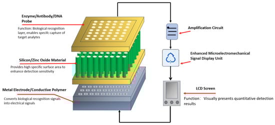
Figure 2.
Schematic Diagram of the Nanowire Biosensor Structure.
Table 2.
Performance Comparison of Nanowire Biosensors.
Table 2.
Performance Comparison of Nanowire Biosensors.
| Material | Mechanism | Target | Concentration Range | Limit of Detection | Sensitivity | Testing Conditions | Reference |
|---|---|---|---|---|---|---|---|
| Silicon NWs | Fluorescence Signal | Gamma-Aminobutyric Acid (GABA) | 970 fM–7 μM | 9.7 μM | / | Room temperature; excitation wavelength: 488 nm | [59] |
| Pt-Au NWs | Cyclic Voltammetry | Penicillin and Tetracycline | 300–240 μM 300–210 μM | 41.2 μA μM−1 cm−2 26.4 μA μM−1 cm−2 | 41.2 μA μM−1 cm−2 26.4 μA μM−1 cm−2 | Room temperature; applied potential: 0–1.2 V | [56] |
| Ru@V2O4 Nanowires | Colorimetric sensors | Cysteine | 3–50 μM | 0.139 μM | / | Room temperature; reaction time: 10 min | [57] |
| Cu2O/Cu@C Core–Shell NWs | Amperometry | Uric Acid | 0.05–1.15 mM | 330.5 μA mM−1 cm−2 | 330.5 μA mM−1 cm−2 | applied potential: +0.4 V | [60] |
| Rutile/Anatase TiO2 (R/A-TiO2) | Photoelectrochemical Biosensor | Glucose | 1–20 mM | 0.019 mM | 5.71 μA·mM−1·cm−2 | applied bias: +0.4 V | [61] |
| Mo-W-ONWs Embedded in Graphene | Electrochemical Sensor (Cyclic Voltammetry, Differential Pulse Voltammetry (DPV)) | Dopamine and Tyrosine | 0.001–48.0 μM 0.001–478.0 μM | 0.8 nM 1.4 nM | 12.3 μA μM−1 cm−2 8.9 μA μM−1 cm−2 | DPV potential range: 0–0.6 V | [62] |
| CuO/Cu2O NWs | Photoelectron chemistry | tyrosinase | 0.05–10 U/mL | 0.016 U/mL | 2.1 μA·(U/mL)−1·cm−2 | UV light irradiation (λ = 365 nm); applied bias: +0.5 V (vs. Ag/AgCl) | [63] |
This enables intuitive quantitative presentation to the user via the display unit, thereby completing precise detection and analysis of the target analyte [43].
During biosensor construction, precise control over nanowire dimensions and aspect ratios typically necessitates a post-synthesis heat treatment stage. As documented in references [53,54,55,56], this stage frequently involves a self-limiting oxidation process. Currently, the three primary methods for nanowire fabrication include suspension techniques, electrochemical deposition, and vapor deposition [52]. Following initial synthesis, these methods may require thermal treatment to fine-tune nanowire structure and properties, ensuring efficient and accurate biosensor operation.
Through integration of biorecognition molecules/elements capable of specific target identification (e.g., glucose, lactose, enzymes, DNA, RNA, or viruses) with sensor technologies possessing energy conversion capabilities, the system can monitor physiological changes as well as chemical and biological constituents in the environment while recording relevant data. These devices exhibit diverse designs and dimensions, enabling detection of ultra-low concentrations of disease biomarkers, hazardous chemicals, and pH fluctuations.
Based on the analyte type or detection signal modality, these devices are categorized into multiple classes, each optimized for specific application scenarios. With technological advancements, their applications in healthcare, food safety, and environmental monitoring continue to expand [53,54,55].
4.1.2. Detection of Neurotransmitters and Organic Molecules
Biosensors, as a high-precision detection technology, have demonstrated indispensable roles in multiple critical fields, including environmental monitoring, food safety, and medical diagnostics. This technology enables highly selective detection of key chemical substances such as dopamine, glucose, and cholesterol [45,46].
- (a)
- Detection of penicillin and tetracycline
To achieve simultaneous detection of penicillin and tetracycline, researchers developed a hybrid nanowire/nanoparticle array electrochemical biosensor incorporating multiple biomolecular sensing elements. In this system, penicillinase was first immobilized onto gold nanoparticles (NPs) via the cross-linking action of 1-ethyl-3-(3-dimethylaminopropyl)carbodiimide (EDC) and N-hydroxysuccinimide (NHS). Subsequently, a monolayer was formed on Pt nanowire segments through electroless plating using L-cysteine, serving as the bioreceptor for tetracycline detection. These nanowire segments were deposited onto discrete gold segments. Furthermore, vertically aligned Pt-Au nanowire arrays were fabricated within anodic aluminum oxide templates using electrodeposition technology [56].
The integrated design leverages the distinct functionalization on Au and Pt segments, allowing the sensor to operate via separate recognition pathways for each antibiotic. Upon exposure to a sample containing both analytes, the immobilized penicillinase catalyzes the hydrolysis of penicillin, while L-cysteine on the Pt nanowires selectively complexes with tetracycline, each generating measurable electrochemical signals.
This multifunctional biosensor array enables efficient simultaneous detection of both antibiotics. The electrode, composed of gold (Au) functionalized with L-cysteine and Pt conjugated with penicillinase, confers dual detection capability for tetracycline and penicillin while exhibiting exceptional sensitivity. Specifically, the electrode demonstrated sensitivities of 41.2 A·μM−1·cm−2 for penicillin and 26.4 A·μM−1 cm−2 for tetracycline. Researchers also analyzed the influence of different segment lengths on sensitivity. During practical sample testing using chicken and beef extracts, the electrode exhibited favorable recovery rates, validating its effectiveness for real-world applications [56,58].
- (b)
- Glucose detection
One-dimensional TiO2 nanorods are regarded as highly promising materials in the field of photoelectrochemical (PEC) biosensors, primarily owing to their efficient electron transport properties, which help reduce the recombination of photogenerated electrons and holes [64]. Vertically aligned one-dimensional TiO2 nanorod arrays grown directly on various transparent conductive substrates exhibit numerous advantages, including a high specific surface area, rapid charge transfer, and enhanced light absorption due to light scattering effects [65]. A technique developed by Liu and Aydil has become one of the widely adopted methods for preparing rutile-phase TiO2 nanorod arrays, particularly on fluorine-doped tin oxide (FTO) substrates [66]. This technique not only ensures robust bonding between the nanorod arrays and FTO substrates but also provides a direct pathway for photogenerated electrons to reach the electron acceptor. Nevertheless, the insufficient charge separation in single-phase TiO2 nanorod arrays remains a significant weakness [67,68,69]. Clearly, further efforts are required to effectively suppress electron-hole recombination.
Building on previous research findings [70,71,72] combining two distinct semiconductor materials can optimize interfacial charge separation efficiency, attributed to their unique band positions and bandgap energies. Integrating anatase and rutile phases—the two most common TiO2 polymorphs in photoelectrochemical applications—effectively reduces charge recombination, thereby enhancing photocatalytic activity [73]. Utilizing this strategy has yielded significant achievements in multiple application fields, such as water splitting reactions [74], solar cells [75], and photodetectors [76]. Typically, the conduction band of rutile TiO2(R-TiO2) lies at a lower energy level than that of anatase TiO2(A-TiO2), while their valence bands are relatively close. This energy level difference may serve as the key driving force for carrier separation. When rutile/anatase TiO2(R/A-TiO2) heterostructures are activated under light illumination, photogenerated electrons migrate from the conduction band of A-TiO2 to that of R-TiO2.
Here, a novel PEC biosensing platform for glucose detection is developed by immobilizing glucose oxidase (GOx) on R/A-TiO2 heterostructures. The high surface area and unique hierarchical morphology of this structure facilitate enzyme immobilization and loading [77]. Optimized electron transfer pathways combined with appropriate heterostructure design enable smoother electron transport to the electrode surface. Compared to single-phase TiO2 nanorod arrays, R/A-TiO2 heterostructures demonstrate superior performance in PEC biosensing applications.
Field emission scanning electron microscopy (FESEM) analysis revealed the fine morphology and nanostructure of the samples. R-TiO2 nanorods, grown directly on the FTO substrate via a secondary hydrothermal method, exhibited diameter distributions in the range of 50–100 nm. Subsequent secondary hydrothermal treatment led to the growth of A-TiO2 nanowires, approximately 5 nm in diameter, on the tips of the R-TiO2 nanorods. These A-TiO2 nanowires combined with the R-TiO2 nanorods to form a tree-like branched architecture, with the A-TiO2 nanowires acting as fine branches and the R-TiO2 nanorods serving as robust trunks. The overall TiO2 film had a thickness of approximately 2 μm. This well-designed structure facilitated rapid electron transport between the R-TiO2 nanorods and the FTO substrate. The heterostructure not only increased the number of active sites but also provided more active lattice facets due to the fine dimensions of the A-TiO2 nanowires [61]. Building upon this, a PEC system for glucose detection was successfully constructed by modifying glucose oxidase (GOx) onto the R/A-TiO2 heterostructure array [67].
Ultraviolet-visible diffuse reflectance spectroscopy (UV-Vis DRS) was employed to investigate the light absorption properties of the R/A-TiO2 heterostructure. Detailed analysis of its light absorption performance was conducted across the wavelength range of 300 to 800 nm [61]. This enhanced visible light absorption is likely attributed to light scattering effects within the hierarchical structure. The improved light absorption contributes to providing greater kinetic energy for enzymatic reactions [78].
The researchers loaded glucose oxidase onto the R/A-TiO2 electrode, thereby applying this heterostructured nanotree array electrode for glucose detection. The standard procedure involved drop-casting 10 μL of a 10 mg/mL glucose oxidase solution, pre-dissolved in 1% sodium chloride, onto the FTO electrode. Time-dependent photocurrent measurements were performed on the electrode at different glucose concentrations (1 to 20 mM). A fixed bias voltage of +0.4 V, as mentioned in a previous study involving glucose detection via a PEC biosensor in 0.1 M PBS, was applied throughout the experiments 60 [79].
The results indicated that the photocurrent displayed high stability at all glucose concentrations and responded rapidly to on/off irradiation cycles within the 1 mM to 20 mM range, confirming the efficient PEC performance of the sensor. Furthermore, a significant correlation coefficient of 0.995 was observed between the photocurrent and glucose concentration across the 1 to 20 mM range. This indicates an excellent sensitivity for electron transfer of 5.71 μA mM−1 cm−2 and a low detection limit of 0.019 mM for glucose (signal-to-noise ratio = 3) [61].
4.2. Strain Sensor
A strain sensor refers to a device that undergoes deformations such as stretching, bending, twisting, or compression when subjected to external stress. This deformation induces microstructural changes within the device, leading to alterations in its electrical characteristics. Upon stress removal, the sensor recovers to its original state [79]. This process converts mechanical signals into electrical signals. Based on the transduction mechanism from input stimulus to output signal, strain sensors are categorized into resistive [80,81], capacitive [82,83], piezoelectric [84], and triboelectric types [85]. Piezoelectric and triboelectric strain sensors typically operate at high frequencies. Due to rapid charge transfer, they cannot capture static strain, and their practical application in multi-scale and wearable strain sensing remains questionable [64]. On the other hand, resistive and capacitive strain sensors have been extensively studied in recent years for wearable electronics due to their relatively simple readout, high stretchability, acceptable dynamic performance, and straightforward fabrication processes. The following sections primarily elaborate on the research status of flexible strain sensors from these aspects: response mechanisms, material systems, device architectures, fabrication techniques, and current research limitations [86].
In the field of flexible strain sensor research, scientists and engineers are dedicated to enhancing sensor performance through novel composite materials and innovative structural designs. These sensors find broad applications in biomedical monitoring, motion tracking, industrial control, and other fields, demonstrating significant market potential. However, despite notable research progress, flexible strain sensors still require improvement in key performance metrics such as sensitivity and detection range [68].
Currently, the primary challenge lies in enhancing sensor sensitivity and broadening the detection range. Typically, these two performance indicators are difficult to optimize simultaneously: sensors with high sensitivity often function only within small to moderate strain ranges, while those covering wide strain ranges may exhibit insufficient sensitivity. This limitation arises because different physical mechanisms—such as sliding fractures, tunneling effects, or crack propagation—predominantly operate within smaller strain ranges, whereas large-strain detection relies more heavily on geometric effects [69].
Another issue is the excessive variation in the gauge factor (sensitivity factor) of highly sensitive sensors across different strain levels. Particularly in the latter half of the sensing range, where the elastomer approaches fracture or resistance increases drastically, the gauge factor can be significantly higher—by several orders of magnitude—than its value at low strains [69]. Therefore, maintaining linearity in sensitivity variation throughout the sensing range and minimizing gauge factor disparities across different strain intervals are critical problems requiring resolution in current research [87].
Nanowires—renowned for their exceptional electrical conductivity and mechanical robustness—are widely recognized as ideal building blocks for high-performance flexible strain sensors, their one-dimensional (1D) geometry inherently enabling efficient charge transport and structural adaptability under deformation. Driven by advances in nanomanufacturing, researchers have explored a spectrum of nanowire morphologies tailored to strain sensing, including discrete individual nanowires, hollow architectures (e.g., carbon nanotubes, CNTs), ordered arrays, and random networks, each engineered to balance sensitivity, stretchability, and scalability [88]. Among these, electrochemically deposited AgNW networks—characterized by high-density, fine-scale interconnections—exhibit a relatively high gauge factor (GF) but are constrained by limited stretchability. In contrast, hydrothermally grown poly(3,4-ethylenedioxythiophene):poly (styrenesulfonate) (PEDOT:PSS) nanowire arrays, with their well-defined aspect ratios, deliver improved stretchability alongside moderate GF yet suffer from poor batch-to-batch consistency. By comparison, silicon nanowires (SiNWs) synthesized via PECVD—leveraging high-purity vapor-phase growth to form crystalline structures—boast an exceptionally high GF but are hindered by inherent brittleness that restricts deformability [89,90].
To precisely respond to minute mechanical stimuli during human motion, researchers have developed ultrasensitive wearable strain sensors based on nanowire arrays. Specifically, they fabricated poly(3,4-ethylenedioxythiophene): poly (styrenesulfonate) (PEDOT:PSS) nanowire arrays via capillary lithography, integrated them into strain sensors, and embedded the devices onto flexible substrates (e.g., PET) [72,73,74,75,76]. The aligned nanowire arrays enable bending signal amplification for reliable sensing responses, endowing the sensors with high sensitivity, distinct responsiveness to microstimuli, fast response speed, good mechanical stability, low hysteresis, and low power consumption. Additionally, the ordered structure ensures geometric uniformity across the sensing area, reducing inter-device performance variations [77]. Besides uniform arrays, nanowire networks also serve as an effective approach to manufacturing high-performance flexible strain sensors.
4.3. Racetrack Resonator Optical Sensor
In cutting-edge research exploring SiNW waveguides, a research team successfully developed a novel optical router based on the principle of a directional coupler, as described in reference [78]. This innovative device achieved significant performance improvements, exhibiting an insertion loss as low as 1.3 dB. In this design, the router’s cross-section ingeniously incorporated three parallel SiNWs, each with a diameter of 100 nm and uniformly spaced 200 nm apart, resulting in an overall height of 600 nm. In directional couplers, bending loss is not a concern since they contain no bends. However, in the current work, a SiNWs sensor utilizing a ring resonator mechanism is being developed. Consequently, bending loss must be considered. When optimizing optical waveguide design, a common strategy involves increasing the amount of silicon material and reducing free-space regions to minimize power radiation at waveguide bends, thereby reducing bending loss. Specifically, this may involve increasing the number of spiral turns, enlarging their diameter, or decreasing the spacing between spirals. In this process, a balance must be struck between bending loss and sensor sensitivity. On one hand, increasing the gaps and reducing silicon enhances the interaction between photonic modes and the analyte, improving sensor sensitivity, but this may come at the cost of increased bending loss. On the other hand, reducing gaps and increasing silicon effectively lowers bending loss but may sacrifice sensor sensitivity. Therefore, careful trade-offs between these two factors are essential in the design [91,92,93,94].
The research team has introduced an innovative design for a silicon nanowire optical sensor. This sensor employs meticulously arranged silicon nanowires configured into a ring resonator structure, where the cladding of the nanowires and the gaps between them are filled with the substance to be analyzed [79,80,81,82]. This sensor is distinguished by its compact footprint of 16 μm × 16.5 μm and an exceptionally low insertion loss of 0.4 dB. A bending radius of 8 μm was selected, yielding an insertion loss of 0.4 dB and dimensions of 16 μm × 16.5 μm. Figure 3a illustrates the 3D design of the silicon nanowire ring resonator, while Figure 3b shows its cross-section. The refractive indices used were 1.45 for SiO2 and 3.45 for Si, while the indices for the gaps and cladding were initially set to 1 at λ = 1.55 μm. The bus waveguide width and height were 100 nm and 600 nm, respectively. The SiO2 thickness was 3 μm.
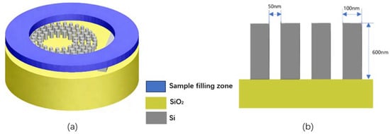
Figure 3.
Schematic structure of vertical silicon nanowire racetrack resonator optical sensor (a) Perspective view; (b) Cross-sectional view. Figure redrawn from reference [95].
Different fabrication methods have been proposed for this purpose. On SOI chips with a 600 nm-thick device layer, silicon nanowire patterns are defined through electron-beam lithography or nanosphere lithography techniques, followed by deep reactive-ion etching (DRIE) processing [92,93]. The fabrication process involves three primary approaches: In the first approach, photoresist is coated onto the SOI wafer device layer, selectively exposed via electron-beam writing or UV exposure through a mask, and developed to remove unexposed regions, forming the desired pattern; DRIE is subsequently employed to create vertically aligned silicon nanowire structures. Alternatively, the second method utilizes UV exposure through a mask to pattern the photoresist, followed by development to remove unexposed areas, with DRIE then forming the vertical nanowire configuration. The third approach entails depositing nanospheres onto photoresist, patterning through development to eliminate unexposed regions between nanospheres, removing the nanospheres via oxygen plasma etching, and finally applying DRIE to fabricate vertically oriented silicon nanowire structures. These procedures collectively constitute the precision manufacturing process for silicon nanowires.
Research findings indicate that a previously reported silicon nanowire (SiNWs) sensor [83,84,85,86] utilized a ring resonator design, achieving a sensitivity of 243 nm per refractive index unit (RIU). This sensor incorporated nanowires with the following parameters: nine nanowires of 50 nm diameter, 75 nm pitch, and 700 nm height. However, an alternative design measuring 16 μm × 16.5 μm with an exceptionally low insertion loss of 0.4 dB demonstrated significantly enhanced sensitivity of 430 nm/RIU [87,88,89,90]. This configuration maintained the 0.4 dB insertion loss while implementing an 8 μm bending radius within the same 16 μm × 16.5 μm footprint. Such performance represents a notable achievement in optical sensing technology [93,95].
4.4. Pressure Sensor
Pressure sensors represent another crucial branch in mechanical sensing, particularly distinguished by their high sensitivity to longitudinal responses to mechanical forces. To fabricate flexible piezoresistive pressure sensors, nanowires with diverse architectures can be incorporated into elastic polymers, hydrogels, or onto flexible substrates as conductive fillers or functional sensing elements. Upon stimulation by external pressure, these conductive fillers exhibit significantly enhanced electrical conductivity, thereby enabling precise pressure detection.
- (a)
- PU/Ag NWs (Polyurethane/Silver Nanowires)
PU/Ag NWs (polyurethane/silver nanowire) composite functional membranes can serve as pressure sensors, comprising two layers of PU/Ag NWs films arranged with their microstructured surfaces facing each other. In this configuration, patterned Ag NWs deposited on dome-structured surfaces act as conductive fillers, forming a non-uniform conductive network that enables highly sensitive sensing [90,91]. Similarly, researchers [92,93,94,95,96] reported a method involving the coating of vertically aligned silver nanowires (AgNWs) on ordered micropyramid arrays to fabricate high-performance wearable pressure sensors.
Typically, vertically aligned AgNW microarrays are grown on PDMS (polydimethylsiloxane) films with pyramidal microstructures via a modified seed-mediated growth approach. This integration of hierarchical micropyramid structures with vertical nanowires facilitates the production of high-performance flexible pressure sensors. Such sensors exhibit sufficiently high sensitivity (~23 kPa−1) in the low-pressure regime (<600 Pa), rapid response/recovery times (<10 ms) during loading/unloading cycles, and exceptional stability over 10,000 compression cycles [97,98]. Furthermore, other bioinspired structural designs—such as micropore arrays and micropillar arrays—can be incorporated into flexible pressure sensors to achieve high sensitivity and favorable signal-to-noise ratios. This enhanced performance arises from significant resistance changes caused by rough or uneven contact between functional layers and electrodes due to surface topography. Additionally, combining nanowires with other functionally layered materials further augments pressure sensor capabilities [99]. Generally, integrating nanowires with two-dimensional graphene generates synergistic effects that confer superior electrical properties compared to sensors fabricated solely from metallic nanowires. For instance, an ultrathin flexible piezoresistive skin sensor based on a hierarchical nanonetwork composite of silver nanowires, graphene, and polyamide nanofibers (PANFs) demonstrates both high sensitivity and a broad pressure-sensing range [100].
- (b)
- Flexible p-GaN thin film/n-ZnO nanostructures
Sensors emulating human tactile perception play pivotal roles in domains such as health and environmental monitoring, human–machine interaction, and next-generation robotics. Such sensors necessitate critical characteristics, including high spatial resolution, rapid response capability, high sensitivity, and large-scale integration capacity [101,102,103,104,105,106]. Researchers have developed diverse tactile sensors based on resistive or capacitive variations that respond to external pressure changes. These devices are typically fabricated using conductive elastomeric composites (e.g., hybrid rubbers incorporating single-walled carbon nanotubes) or microstructured elastic dielectric layers (often integrated with field-effect transistors), achieving millimeter-scale resolution [107,108,109]. To meet the requirement for spatial resolution exceeding 50 μm in electronic skin (mimicking human skin), a research team proposed a pressure sensor array based on ZnO nanowire/p-GaN LED structures. Leveraging the piezophototronic effect, this array achieves precise mapping of two-dimensional pressure distribution with spatial resolution as fine as 2.7 μm [80].
To address the insufficient flexibility of rigid substrates, researchers have developed flexible pressure sensor arrays based on hybrid inorganic materials (such as ZnO and CdS nanowires) and organic materials (PEDOT:PSS), utilizing the piezophototronic effect for pressure sensing [110,111,112,113,114,115]. However, compared to GaN-based sensors, these flexible devices suffer from limitations, including low resolution, poor stability, short lifespan, and challenges in achieving epitaxial nanowire growth.
A critical breakthrough emerged through combining the advantages of GaN-based sensors with flexible characteristics. Although the GaN/sapphire structure exhibits rigidity due to its 500-μm-thick sapphire substrate, the 5-μm-thick GaN layer itself possesses intrinsic flexibility. By delaminating the GaN thin film and integrating it with ZnO nanowire arrays, researchers achieved the first demonstration of direct ZnO nanowire growth on flexible GaN. This advancement enabled the successful development of high-resolution flexible GaN/ZnO LED pressure sensors [116].
The fabrication of flexible GaN thin films commenced with the epitaxial growth of a 2.5-μm undoped GaN buffer layer and a 2.5-μm Mg-doped p-type GaN layer on sapphire substrates via metalorganic chemical vapor deposition (MOCVD). A 20 nm Ni/100 nm Au sacrificial layer was deposited by magnetron sputtering (Kurt J. Lesker, PVD75), followed by electroplating of a 50-μm Cu support layer. Laser lift-off (LLO) was performed using a 248 nm KrF laser (254 mJ/cm2) to separate the sapphire substrate, with subsequent hot pressing at 423 K for 30 min ensuring film flatness [117]. To address backside defects, a 200-μm PET film was bonded to the GaN backside using epoxy resin while maintaining frontside exposure for device processing. The structure was cured in a 373 K oven for 2 h, followed by wet etching to remove the Cu/Au/Ni sacrificial layers, yielding a transparent and damage-free flexible GaN substrate.
For ZnO nanowire synthesis, photolithography first defined array patterns with 300-μm linewidth and 30-μm pitch. A bottom-gate electrode was formed by DC magnetron sputtering of 10 nm Ni and 25 nm Au layers. After photoresist removal, SU-8 photoresist lithography created cylindrical arrays (2-μm diameter, 5-μm pitch). A 35 nm SiO2 mask layer was deposited via RF magnetron sputtering, with residual photoresist subsequently removed [118]. Finally, the SiO2-patterned flexible GaN substrate underwent hydrothermal reaction in a solution containing 40 mM hexamethylenetetramine and 40 mM zinc nitrate at 85 °C for 4 h, resulting in vertically aligned ZnO nanowire arrays [80,119].
Within the nutrient solution, centimeter-scale uniformly distributed ZnO nanowire arrays were epitaxially grown on the c-axis-oriented GaN surface. SU-8 photoresist was subsequently spin-coated to encapsulate the nanowires, followed by oxygen plasma etching to expose the nanowire tips. Finally, a 300 nm ITO layer was sputtered to form the top common electrode, completing the fabrication of the flexible heterojunction device.
This flexible and stable LED-based pressure sensor array, composed of p-GaN/n-ZnO nanowire heterostructures, achieves high spatial resolution (2.6 μm, significantly surpassing the 50 μm resolution of human skin) and rapid response time (180 ms) for pressure distribution mapping, meeting artificial skin performance requirements. Strain-induced polarization charges effectively reduce the localized surface barrier height on the ZnO side, thereby enhancing luminescence through the piezophototronic effect by increasing electron-hole recombination rates. Pressure distribution is obtained by parallel detection of varying electroluminescence (EL) emission intensities from the LED array [116,120].
4.5. Gas Sensor
ZnO, an oxide semiconductor with exceptional physicochemical properties, is widely employed as a gas-sensing material in the field of gas sensors [120,121,122]. As a representative II-VI group direct bandgap semiconductor, ZnO exhibits a wide bandgap (3.37 eV), large exciton binding energy (60 meV), and high electron mobility (~400 cm2 V−1 s−1) [101]. Additionally, ZnO possesses advantages including excellent biocompatibility, chemical stability, environmental friendliness, and low cost, establishing it as a prominent material for detecting toxic and hazardous gases [123]. Studies on gas-sensing characteristics reveal that the microscopic morphology of sensing materials significantly influences sensing performance. Sonalika Agarwal et al. synthesized flower-like ZnO hierarchical nanostructures and nanoflower-assembled ZnO nanorods via hydrothermal methods, investigating the impact of microstructure on gas-sensing properties [124].
According to the provided data, ZnO and TiO2 nanowires have been successfully fabricated on silicon micropillars with varying diameters and heights. Specifically, silicon micropillars measuring 400 nm in diameter and 1.5 μm in height exhibit an aspect ratio of 1.5 μm/400 nm = 3.75, while those with 600 nm diameter and 3.2 μm height demonstrate an aspect ratio of 3.2 μm/600 nm ≈ 5.33. Consequently, the 600 nm-diameter, 3.2 μm-height silicon micropillars possess a greater aspect ratio.
This increased spacing facilitates the growth of TiO2 and ZnO nanowires with larger diameters and enhanced crystallinity, which is more advantageous for gas sensing applications. Consequently, researchers selected the 600 nm-diameter, 3.2-μm-height silicon micropillars as substrates for growing ZnO nanowires (60 min growth) and TiO2 nanowires (3 h growth) specifically for gas sensor development [13].
Investigations into the gas-sensing properties of ZnO nanowire/TiO2 nanowire/Si micropillar structures were conducted using a laboratory-built testing apparatus. This system comprised a sealed test chamber, heating equipment (hot plate), and data acquisition instruments. Gas-sensing performance was evaluated in an ambient atmosphere, with alcohol vapor concentrations controlled by injecting precise quantities of liquid alcohol through an inlet port. After sufficient reaction time, ambient air was introduced through a vent to purge alcohol vapors from the chamber [125].
When alcohol molecules enter the sensor, ZnO and TiO2 nanostructures adsorb these molecules and release electrons, causing a sharp decrease in resistance. As environmental alcohol concentration decreases, the adsorbed molecules desorb from ZnO and TiO2, allowing resistance to gradually recover to its initial value. The gas response (S) is defined by the formula: (Rair − Rgas)/Rgas, where Rgas represents resistance in a gas atmosphere and Rair denotes resistance in air.
In this work, each response-recovery cycle comprised eight injection periods with 120 s response and 120 s recovery times. According to Table 1, the ZnO nanowire/Si micropillar sensor exhibited an average Rair of 231 Ω in air, decreasing to Rgas = 164 Ω upon ethanol exposure, yielding a response value S of 40.9% calculated as (231 − 164)/164. Conversely, the ZnO/TiO2/Si micropillar sensor showed Rair = 1460 Ω in air and Rgas = 825 Ω in an ethanol atmosphere, resulting in S = 77.0%. This indicates significantly enhanced response performance in the ZnO/TiO2/Si micropillar sensor compared to the ZnO/Si micropillar configuration under identical testing conditions [105].
The ZnO nanowire/TiO2 nanowire/Si micropillar configuration demonstrates significant advantages over the ZnO nanowire/Si micropillar structure. Firstly, both TiO2 and ZnO nanowires function as sensing materials with distinct gas sensitivities, endowing the ternary structure with broader application potential. Secondly, the enlarged surface area provided by the ZnO/TiO2/Si micropillar architecture enhances gas-material interactions, thereby improving ethanol response performance. Consequently, this configuration exhibits superior capabilities for ethanol concentration detection. In this work, ZnO and TiO2 nanowires were successfully fabricated on silicon micropillars, establishing the novel ZnO/TiO2/Si micropillar structure for its first application in gas sensing [105,106,107,108,109,110].
When examining the research and applications of nanowire sensors, it is noted that their designs and operational domains span diverse fields from environmental monitoring to biological detection. To comprehensively evaluate their performance across applications, comparative analysis of measurement parameters and sensitivity characteristics is essential [110,111,112,113,114,115]. As detailed earlier, these specifications are systematically presented in Table 3. Subsequent examination of Table 3 enables further analysis of distinct performance metrics across application domains and sensitivity profiles for specific measurement tasks, providing a holistic perspective for selecting optimal nanowire sensors tailored to particular applications.
Table 3.
Industrialization Potential of Nanowire Sensors.
5. Economic and Technical Feasibility
The evolving demands for sensing technologies and concurrent advancements in nanomaterials science have collectively propelled the transition of nanowire sensors from laboratory research to industrial application [116,117,118,119]. Contemporary fabrication techniques, including hydrothermal synthesis, magnetron sputtering, and electrochemical deposition, now enable the reliable construction of sensitive nanostructures characterized by high specific surface area and unique electronic properties. These developments establish a robust technical foundation for high-performance sensing applications. Research demonstrates that specific nanowire configurations, such as ZnO/TiO2 heterojunctions and p-GaN/n-ZnO structures, exhibit exceptional capabilities in gas detection, pressure sensing, and biomolecular recognition. Their performance metrics—including sensitivity, response speed, and resolution—surpass those of conventional sensors by several orders of magnitude [119,120,121,122,123].
Despite this significant potential, the full commercial translation of nanowire sensors remains an ongoing endeavor [123,124]. To bridge the gap between high-performance prototypes and commercially viable products, industry stakeholders are pursuing continuous material optimization and process innovations to enhance reliability and reduce costs. Notably, the production cost of silver nanowires has decreased by over 70% within the past five years. Companies such as Suzhou Nuofei have established scaled production lines, enabling the cost-effective mass adoption of nanowire touch sensors in consumer electronics [126]. Furthermore, the maturation of next-generation fabrication technologies, particularly nanoimprinting and roll-to-roll manufacturing, provides a clear pathway for achieving additional cost reductions exceeding 50% within the next three to five years.
These technological advancements are accelerating the penetration of nanowire sensors into high-value market segments. The global market reached $1.2 billion in 2023, expanding at a compound annual growth rate of 32%, with medical diagnostics (45%), environmental monitoring (28%), and industrial control (18%) representing the dominant application areas. Through sustained technical refinement and cost optimization, nanowire sensors are poised for large-scale integration into trillion-dollar markets, including smart homes and wearable devices, thereby completing the crucial transition from technological superiority to tangible commercial value [127].
6. Conclusions
With the rapid advancement of nanomaterial synthesis techniques, one-dimensional (1D) nanostructures such as nanowires (NWs) have garnered significant attention and demonstrated substantial application potential across multiple domains. These assembled 1D nanomaterials have become an emerging focal point in nanotechnology due to their distinctive structure-property relationships.
This review examines the correlation between structure and properties in assembled NWs materials, highlighting recent progress and representative examples in this research field. It summarizes ordered NW architectures exhibiting anisotropic characteristics, including anisotropic conduction, optical anisotropy, thermal anisotropy, magnetic anisotropy, and anisotropic strain sensing. These properties originate from the abundance of transport pathways in 1D nanomaterials, which guide electrons, phonons, and ions along their longitudinal axes, enabling efficient transport media. Transport velocity can be optimized by altering the transport direction.
Beyond structural features, the review emphasizes the critical importance of performance enhancement in ordered 1D nanomaterial-based devices. For instance, the resistance of metallic NWs films primarily depends on junction resistance, which typically substantially exceeds the intrinsic resistance of individual NWs. Aligning NWs along a uniform orientation significantly reduces junction resistance, thereby enhancing the conductivity of NWs devices. The spatial arrangement of NWs networks can also be modulated through alignment. Precise microstructural design enables tunable interactions between 1D nanomaterials.
Ultimately, the review underscores that advanced assembly methods allow predefined structuring and functionality in NWs devices. For example, forming ordered NWs patterns on substrates facilitates integrated circuit construction for specific functionalities. All enhanced properties achieved through ordered assembly are comprehensively summarized, confirming that such ordered configurations offer promising prospects for commercial NWs device applications.
Author Contributions
C.P.: Conceptualization, Investigation, Methodology, Writing—original draft. Y.Z.: Investigation, Visualization. J.Z. (JianXing Zhao): Investigation, Methodology. A.W.: Conceptualization, Investigation. J.Z. (JianHong Zhou): Formal analysis, Writing—review & editing. C.W.: Supervision, Project administration, Writing—review & editing. All authors have read and agreed to the published version of the manuscript.
Funding
This work was funded by the National Natural Science Foundation of China (Grant No. 12274042).
Data Availability Statement
No new data were created or analyzed in this study. Data sharing is not applicable to this article.
Conflicts of Interest
The authors declare no conflicts of interest.
References
- Bhatt, V.; Kumar, M.; Choi, M.-J.; Yun, J.-H. Role of Cu2+/Cu1+ induced adsorbed oxygen species in SnO2 nanocrystals for H2S gas detection at ppb level. Int. J. Hydrogen Energy 2025, 112, 482–492. [Google Scholar] [CrossRef]
- Shaik, R.; Kampara, R.K.; Kumar, A.; Sharma, C.S.; Kumar, M. Metal Oxide Nanofibers Based Chemiresistive H2S Gas Sensors. Coord. Chem. Rev. 2022, 471, 214752. [Google Scholar] [CrossRef]
- Ruksana, S.; Kumar, A.; Lakshmy, S.; Kishore, K.R.; Sharma, C.S.; Kumar, M.; Chakraborty, B. Highly Efficient CuO-Anchored SnO2Nanofiber for Low-Concentration H2S Gas Sensors. ACS Appl. Eng. Mater. 2024, 2, 431–442. [Google Scholar] [CrossRef]
- Zhang, X.; Hao, X.; Zhai, Z.; Wang, J.; Li, H.; Sun, Y.; Qin, Y.; Niu, B.; Li, C. Flexible H2S Sensors: Fabricated by Growing NO2-UiO-66 on Electrospun Nanofibers for Detecting Ultralow Concen-tration H2S. Appl. Surf. Sci. 2022, 573, 151446. [Google Scholar] [CrossRef]
- Kumar, S.; Chaurasiya, R.; Khan, M.A.; Meng, G.; Chen, J.-S.; Kumar, M. Enhancement of H2S Sensing Performance of RGO Decorated CuO Thin Films: Experimental and DFT Studies. J. Phys. Condens. Matter 2023, 35, 064001. [Google Scholar] [CrossRef]
- Kumar, A.; Shringi, A.K.; Kumar, M. RF Sputtered CuO Anchored SnO2 for H2S Gas Sensor. Sens. Actuators B Chem. 2022, 370, 132417. [Google Scholar] [CrossRef]
- Teng, Y.; Zhang, X.F.; Xu, T.T.; Deng, Z.P.; Xu, Y.M.; Huo, L.H.; Gao, S. A Spendable Gas Sensor with Higher Sensitivity and Lowest Detection Limit towards H2S: Porous α-Fe2O3 Hierarchical Tubule Derived from Poplar Branch. Chem. Eng. J. 2020, 392, 123679. [Google Scholar] [CrossRef]
- Chowdhuri, A.; Gupta, V.; Sreenivas, K.; Kumar, R.; Mozumdar, S.; Patanjali, P.K. Response Speed of SnO2-Based H2S Gas Sensors with CuO Nanoparticles. Appl. Phys. Lett. 2004, 84, 1180–1182. [Google Scholar] [CrossRef]
- Li, H.; Yang, Z.; Ling, W.; Zhu, D.; Pu, Y. UV Excited Gas Sensing SnO2-ZnO Aerogels to Ppb-Level Ethanol Detection. Sens. Actuators B Chem. 2021, 337, 129815. [Google Scholar] [CrossRef]
- Park, K.R.; Cho, H.B.; Lee, J.; Song, Y.; Kim, W.B.; Choa, Y.H. Design of Highly Porous SnO2-CuO Nanotubes for Enhancing H2S Gas Sensor Performance. Sens. Actuators B Chem. 2020, 302, 127179. [Google Scholar] [CrossRef]
- Lai, T.Y.; Fang, T.H.; Hsiao, Y.J.; Chan, C.A. Characteristics of Au-Doped SnO2-ZnO Heteronanostructures for Gas Sensing Applications. Vacuum 2019, 166, 155–161. [Google Scholar] [CrossRef]
- Yin, X.T.; Li, J.; Wang, Q.; Dastan, D.; Shi, Z.C.; Alharbi, N.; Garmestani, H.; Tan, X.M.; Liu, Y.; Ma, X.G. Opposite Sensing Response of Heterojunction Gas Sensors Based on SnO2-Cr2O3 Nanocomposites to H2 against CO and Its Selectivity Mechanism. Langmuir 2021, 37, 13548–13558. [Google Scholar] [CrossRef] [PubMed]
- Liu, J.; Xu, Y.; Yi, F. Fabrication of the ZnO nanowires/TiO2 nanowires/Si micropillars structures for the gas sensor application. Sens. Actuators A Phys. 2022, 345, 113665. [Google Scholar] [CrossRef]
- Gautam, V.; Kumar, A.; Nagpal, S.; Jain, V.K. Ultrasensitive detection of formaldehyde at room temperature using Si-chip assisted MOS/SiNWs nanocomposite based sensor. J. Alloys Compd. 2022, 919, 165840. [Google Scholar] [CrossRef]
- Wang, J.; Ding, J.; Che, K.; Cui, T.; Wan, Y.; Yang, Z.; Zhang, Q. Constructing a stable high conductive network: Exploring AgNW distribution in bacterial nanocellulose for tunable electromagnetic shielding performance. Carbohydr. Polym. 2026, 372, 124549. [Google Scholar] [CrossRef]
- Wang, L.; Wang, Y.; He, S.; Wen, J.; Du, Q.; Zhang, Y.; Zhang, W.; Gao, R.; Zhang, K.; Cui, R.; et al. A 3D porous AgNWs/graphene/PDMS sensor enabling multifunctional applications for gesture recognition and health monitoring. Chem. Eng. J. 2025, 525, 170111. [Google Scholar] [CrossRef]
- Domansky, K.; Janata, J. Present state of fabrication of chemically sensitive field-effect transistors. Analyst 1993, 118, 335–340. [Google Scholar] [CrossRef]
- Janata, J. 20 Years of ion-selective field-effect transistors. Analyst 1994, 119, 2275–2278. [Google Scholar] [CrossRef]
- Cui, Y.; Zhong, Z.; Wang, D.; Wang, W.U.; Lieber, C.M. High performance silicon nanowire field effect transistors. Nano Lett. 2003, 3, 149–152. [Google Scholar] [CrossRef]
- Jin, S.; Whang, D.; McAlpine, M.C.; Friedman, R.S.; Wu, Y.; Lieber, C.M. Scalable interconnection and integration of nanowire devices without registration. Nano Lett. 2004, 4, 915–919. [Google Scholar] [CrossRef]
- Zheng, G.F.; Lu, W.; Jin, S.; Lieber, C.M. Synthesis and fabrication of high-performance n-type silicon nanowire transistors. Adv. Mater. 2004, 16, 1890–1893. [Google Scholar] [CrossRef]
- Cui, Y.; Wei, Q.; Park, H.; Lieber, C.M. Nanowire nanosensors for highly sensitive and selective detection of biological and chemical species. Science 2001, 293, 1289–1292. [Google Scholar] [CrossRef] [PubMed]
- Hahm, J.; Lieber, C.M. Direct ultrasensitive electrical detection of DNA and DNA sequence variations using nanowire nanosensors. Nano Lett. 2004, 4, 51–54. [Google Scholar] [CrossRef]
- Wang, W.U.; Chen, C.; Lin, K.H.; Fang, Y.; Lieber, C.M. Label-free detection of small-molecule-protein interactions by using nanowire nanosensors. Proc. Natl. Acad. Sci. USA 2005, 102, 3208–3212. [Google Scholar] [CrossRef] [PubMed]
- Wu, J.; Hao, W.; Han, D.; Cai, L.; Guo, M.; Fang, G.; Wang, S. Near-infrared electrochemiluminescence sensor based on magnetic-responsive hydrogel with endogenous luminescent CuNWs@CeVO4 microcapsules for the biomimetic detection of lincomycin. Sens. Actuators B Chem. 2026, 449, 139086. [Google Scholar] [CrossRef]
- Cao, H.; Zhang, Z.; Popov, E.O.; Filippov, S.V.; Kolosko, A.G.; Chen, Y.; Wu, J.; Liu, C.; Zhan, R.; Deng, S.; et al. Field emission from ZnO nanowires with atomic layer deposition coated In2O3 thin films. Vacuum 2026, 246, 115053. [Google Scholar] [CrossRef]
- Beitone, S.; Ternon, C.; Belmouhoub, M.; Rapenne, L.; Coindeau, S.; Ortega, S.; Roussel, H.; Riassetto, D. Mechanisms involved in the hydrothermal growth of thin and long Cu2O nanowires. Mater. Today Chem. 2026, 51, 103250. [Google Scholar] [CrossRef]
- Chang, C.-S.; Li, T.-C.; Tsai, Y.-C.; Wu, G.-H.; Lin, J.-F. Effects of deposition method and conditions for IGZO film and thermal annealing on composite film quality, surface roughness, microstructural defects, and electrical properties of Ti/IGZO/graphene/polyimide specimens. J. Alloys Compd. 2018, 768, 298–315. [Google Scholar] [CrossRef]
- Ismailov, A.M.; Umakhanov, M.A.; Rabadanov, M.R.; Rabadanov, M.K. Epitaxial deposition of β-Ga2O3 films by radio-frequency magnetron sputtering at elevated substrate temperatures. Vacuum 2026, 244, 114840. [Google Scholar] [CrossRef]
- Patolsky, F.; Zheng, G.; Hayden, O.; Lakadamyali, M.; Zhuang, X.; Lieber, C.M. Electrical detection of single viruses. Proc. Natl. Acad. Sci. USA 2004, 101, 14017–14022. [Google Scholar] [CrossRef]
- Wu, T.-H.; Hong, F.C.-N. The growth of axially modulated p–n GaN nanowires by plasma-enhanced chemical vapor deposition. Thin Solid Film. 2013, 529, 128–132. [Google Scholar] [CrossRef]
- Sahoo, S.; Sahoo, G.; Jeong, S.M.; Rout, C.S. A review on supercapacitors based on plasma enhanced chemical vapor deposited vertical graphene arrays. J. Energy Storage 2022, 53, 105212. [Google Scholar] [CrossRef]
- Zheng, G.F.; Patolsky, F.; Cui, Y.; Wang, W.U.; Lieber, C.M. Multiplexed electrical detection of cancer markers with nanowire sensor arrays. Nat. Biotechnol. 2005, 23, 1294–1301. [Google Scholar] [CrossRef] [PubMed]
- Li, G.; Peng, H.; Xue, Y.S.; Qin, W.F. Preparation and Properties of CNTs/AgNWs/CNTs/TPU Nanofiber Membrane Strain Sensors. J. Text. Sci. Eng. 2023, 40, 75–79. [Google Scholar]
- Liu, J.; Yi, F.T. Fabrication and properties of ZnO nanorods on silicon nanopillar surface for gas sensor application. J. Mater. Sci. Mater. Electron. 2019, 30, 11404–11411. [Google Scholar] [CrossRef]
- Zhang, Y.; Zhang, J.; Jin, T.; Xiao, K.; Fang, D.; Wang, J. Preparation of water-soluble ZnS quantum dots by hydrodynamic cavitation technology and related stability exploration. Surf. Interfaces 2025, 72, 106979. [Google Scholar] [CrossRef]
- Wei, H.J.; Xie, Z.M. Application of Electrochemical Deposition Technology in Integrated Circuit Industry. Clean. World 2023, 39, 1–3. [Google Scholar] [CrossRef]
- Liu, J.S. Exploration of Electrochemical Deposition Technology in Preparation of Noble Metal Nanostructures. Metall. Mater. 2024, 44, 94–96. (In Chinese) [Google Scholar] [CrossRef]
- Dadmehr, M.; Allahverdi, M.; Kalat, N.K.; Sheikhnejad, B.; Hosseini, M. Molecular biosensors for detection of miRNA and its application in medical diagnosis. TrAC Trends Anal. Chem. 2026, 195, 118626. [Google Scholar] [CrossRef]
- Nejati, B.; Shadravan, S.; Heidari, M.M.; Etebari, A.; Mobed, A.; Jafarzadeh, S. Innovative approaches to HER2 detection: Biosensors in breast cancer management. Sens. Bio-Sens. Res. 2026, 51, 100948. [Google Scholar] [CrossRef]
- Bocina, E.; Cocuzza, C.; Vincenzi, C.; Fino, D.; Cauda, V.; Piumetti, M. Enzyme-based biosensors: Emerging tools for advanced biomedical applications. Talanta 2026, 300, 129241. [Google Scholar] [CrossRef]
- Guo, H.; Ma, P.; Wang, Z. Fluorescence-enhanced biosensor based on conversion of RNA-to-DNA aptamer for detecting neomycin in food samples. Sens. Actuators B Chem. 2026, 451, 139318. [Google Scholar] [CrossRef]
- Wen, B.; Zhu, Z.; Zeng, J.; Wan, S.; Zhang, C.; Chen, Y.; Wang, L.; Zhang, M.; Yu, K. A ratiometric electrochemical DNA biosensor for the detection of crown-of-thorns starfish eDNA. Bioelectrochemistry 2026, 168, 109162. [Google Scholar] [CrossRef]
- Liu, J. Preparation of ZnO Quantum Dots Composite Membranes via Natural Polymer Electrodeposition and Their Application Research. Master’s Thesis, Wuhan University of Technology, Wuhan, China, 2022. [Google Scholar] [CrossRef]
- Hosseinvand, A.; Ghafourivayghan, M. Biosensor classification and microbiological applications: A food science and packaging perspective. J. Food Eng. 2026, 408, 112899. [Google Scholar] [CrossRef]
- Wali, R.; Moulaee, K.; Qasymeh, M.; Maalej, R.; Neri, G. Atomic layer deposition of NiO-Coated CNT nanocomposites: Tailoring electrochemical properties for salivary lactate detection. J. Electroanal. Chem. 2024, 971, 118594. [Google Scholar] [CrossRef]
- Shyam, S.; Daimary, M.; Narayan, M.; Sarma, H. Biochar-based electroanalytical materials: Towards sustainable, high-performance electrocatalysts and sensors. Next Mater. 2025, 8, 100873. [Google Scholar] [CrossRef]
- Li, Z.; Gao, F.; Gu, Z. Vertically aligned Pt nanowire array/Au nanoparticle hybrid structure as highly sensitive amperometric biosensors. Sens. Actuators B Chem. 2017, 243, 1092–1101. [Google Scholar] [CrossRef]
- Gao, F.; Li, Z.; Ruan, D.; Gu, Z. Synthesis of surface roughed Pt nanowires and their application as electrochemical sensors for hydrogen peroxide detection. J. Nanosci. Nanotechnol. 2014, 14, 6599–6605. [Google Scholar] [CrossRef]
- Li, Z.; Leung, C.; Gao, F.; Gu, Z. Effects of nanowire length and surface roughness on the electrochemical sensor properties of nafion-free, vertically aligned Pt nanowire array electrodes. Sensors 2015, 15, 22473–22489. [Google Scholar] [CrossRef]
- Ruan, D.; Gao, F.; Gu, Z. Enhanced electrochemical properties of surface roughed Pt nanowire electrocatalyst for methanol oxidation. Electrochim. Acta 2014, 147, 225–231. [Google Scholar] [CrossRef]
- Kim, N.; Han, K.; Su, P.-C.; Kim, I.; Yoon, Y.-J. A rotationally focused flow (RFF) microfluidic biosensor by density difference for early-stage detectable diagnosis. Sci. Rep. 2021, 11, 9277. [Google Scholar] [CrossRef]
- Kartashova, A.D.; Gonchar, K.A.; Chermoshentsev, D.A.; Alekseeva, E.A.; Gongalsky, M.B.; Bozhev, I.V.; Eliseev, A.A.; Dy-akov, S.A.; Samsonova, J.V.; Osminkina, L.A. Surface-Enhanced Raman Scattering-Active Gold-Decorated Silicon Nanowire Sub-strates for Label-Free Detection of Bilirubin. ACS Biomater. Sci. Eng. 2022, 8, 4175–4184. [Google Scholar] [CrossRef]
- Wang, J.; Hui, N. Electrochemical functionalization of polypyrrole nanowires for the development of ultrasensitive biosensors for detecting microRNA. Sens. Actuators B Chem. 2019, 281, 478–485. [Google Scholar] [CrossRef]
- Takahashi, H.; Yasui, T.; Klamchuen, A.; Khemasiri, N.; Wuthikhun, T.; Paisrisarn, P.; Shinjo, K.; Kitano, Y.; Aoki, K.; Natsume, A.; et al. Annealed ZnO/Al2O3 Core-Shell Nanowire as a Platform to Capture RNA in Blood Plasma. Nanomaterials 2021, 11, 1768. [Google Scholar] [CrossRef]
- Li, Z.; Liu, C.; Sarpong, V.; Gu, Z. Multisegment nanowire/nanoparticle hybrid arrays as electrochemical biosensors for simultaneous detection of antibiotics. Biosens. Bioelectron. 2019, 126, 632–639. [Google Scholar] [CrossRef]
- Hou, J.; Jia, P.; Yang, K.; Bu, T.; Sun, X.; Wang, L. Facile preparation of Ru@V2O4 nanowires exhibiting excellent tetra-enzyme mimetic activities for sensitive colorimetric H2O2 and cysteine sensing. Sens. Actuators B Chem. 2021, 344, 130266. [Google Scholar] [CrossRef]
- Ambhorkar, P.; Wang, Z.; Ko, H.; Lee, S.; Koo, K.-I.; Kim, K.; Cho, D.-I.D. Nanowire-Based Biosensors: From Growth to Applications. Micromachines 2018, 9, 679. [Google Scholar] [CrossRef]
- Lee, J.-H.; Chae, E.-J.; Park, S.-J.; Choi, J.-W. Label-free detection of γ-aminobutyric acid based on silicon nanowire biosensor. Nano Converg. 2019, 6, 13. [Google Scholar] [CrossRef]
- Luo, J.; Cui, J.; Wang, Y.; Yu, D.; Qin, Y.; Zheng, H.; Shu, X.; Tan, H.H.; Zhang, Y.; Wu, Y. Metal-organic framework-derived porous Cu2O/Cu@C core-shell nanowires and their application in uric acid biosensor. Appl. Surf. Sci. 2020, 506, 144662. [Google Scholar] [CrossRef]
- Yan, B.; Zhuang, Y.; Jiang, Y.; Xu, W.; Chen, Y.; Tu, J.; Wang, X.; Wu, Q. Enhanced photoeletrochemical biosensing performance from rutile nanorod/anatase nanowire junction array. Appl. Surf. Sci. 2018, 458, 382–388. [Google Scholar] [CrossRef]
- Mariyappan, V.; Jeyapragasam, T.; Chen, S.-M.; Murugan, K. Mo-W-O nanowire intercalated graphene aerogel nanocomposite for the simultaneous determination of dopamine and tyrosine in human urine and blood serum sample. J. Electroanal. Chem. 2021, 895, 115391. [Google Scholar] [CrossRef]
- Guo, X.; Wu, J.; Xia, L.; Xiang, M.; Qu, F.; Li, J. CuO/Cu2O nanowire array photoelectrochemical biosensor for ultrasensitive detection of tyrosinase. Sci. China Chem. 2020, 63, 1012–1018. [Google Scholar] [CrossRef]
- Zhao, Z.; Tian, J.; Sang, Y.; Cabot, A.; Liu, H. Structure, Synthesis, and Applications of TiO2 Nanobelts. Adv. Mater. 2015, 27, 2557–2582. [Google Scholar] [CrossRef] [PubMed]
- Wang, L.; Yang, W.; Chong, H.; Wang, L.; Gao, F.; Tian, L.; Yang, Z. Efficient ultraviolet photodetectors based on TiO2 nanotube arrays with tailored structures. Rsc. Adv. 2015, 5, 52388–52394. [Google Scholar] [CrossRef]
- Liu, B.; Aydil, E.S. Growth of Oriented Single-Crystalline Rutile TiO2 Nanorods on Transparent Conducting Substrates for Dye-Sensitized Solar Cells. J. Am. Chem. Soc. 2009, 131, 3985–3990. [Google Scholar] [CrossRef]
- Yu, X.; Zhao, Z.; Zhang, J.; Guo, W.; Qiu, J.; Li, D.; Li, Z.; Mou, X.; Li, L.; Li, A.; et al. Rutile Nanorod/Anatase Nanowire Junction Array as Both Sensor and Power Supplier for High-Performance, Self-Powered, Wireless UV Photodetector. Small 2016, 12, 2759–2767. [Google Scholar] [CrossRef]
- Li, J.; Li, Z.; Lu, Y.; Ye, G.; Hong, Y.; Niu, L.; Fang, J. Research progress of machine learning in flexible strain sensors in the context of material intelligence. Mater. Today Phys. 2025, 59, 101932. [Google Scholar] [CrossRef]
- Khan, A.; Prathumrat, P.; Likitaporn, C.; Wongsalam, T.; Tanalue, N.; Nichakornpong, N.; Okhawilai, M. AgNP-MWCNT nanocomposites for flexible strain sensors: Comprehensive insights into green synthesis, advanced fabrication technologies, and emerging applications. Synth. Met. 2026, 316, 118003. [Google Scholar] [CrossRef]
- Lee, J.-H.; Ko, K.-H.; Park, B.-O. Electrical and optical properties of ZnO transparent conducting films by the sol–gel method. J. Cryst. Growth 2003, 247, 119–125. [Google Scholar] [CrossRef]
- Chen, S.; Qi, Y.; Hisatomi, T.; Ding, Q.; Asai, T.; Li, Z.; Ma, S.S.K.; Zhang, F.; Domen, K.; Li, C. Efficient Visible-Light-Driven Z-Scheme Overall Water Splitting Using a MgTa2O6−xNy /TaON Heterostructure Photocatalyst for H2 Evolution. Angew. Chem. Int. Ed. 2015, 54, 8498–8501. [Google Scholar] [CrossRef]
- Jang, J.S.; Kim, H.G.; Lee, J.S. Heterojunction semiconductors: A strategy to develop efficient photocatalytic materials for visible light water splitting. Catal. Today 2012, 185, 270–277. [Google Scholar] [CrossRef]
- Xiong, Z.; Wu, H.; Zhang, L.; Gu, Y.; Zhao, X.S. Synthesis of TiO2 with controllable ratio of anatase to rutile. J. Mater. Chem. A 2014, 2, 9291–9297. [Google Scholar] [CrossRef]
- Cao, F.; Xiong, J.; Wu, F.; Liu, Q.; Shi, Z.; Yu, Y.; Wang, X.; Li, L. Enhanced Photoelectrochemical Performance from Rationally Designed Anatase/Rutile TiO2 Heterostructures. Acs Appl. Mater. Inter. 2016, 8, 12239–12245. [Google Scholar] [CrossRef] [PubMed]
- Shingai, D.; Ide, Y.; Sohn, W.Y.; Katayama, K. Photoexcited charge carrier dynamics of interconnected TiO2 nanoparticles: Evidence of enhancement of charge separation at anatase–rutile particle interfaces. Phys. Chem. Chem. Phys. 2018, 20, 3484–3489. [Google Scholar] [CrossRef]
- Liu, H.Y.; Liu, G.J. A Comparative Study of Metal–Semiconductor–Metal Ultraviolet Photodetectors Based on Ultrasonic Spray Pyrolysis Deposited Anatase and Rutile TiO2. IEEE Trans. Electron. Devices 2017, 64, 1108–1113. [Google Scholar] [CrossRef]
- Fu, Y.; Wang, X.; Hang, G.; Cao, J.; Wu, X.; Duan, J.; Liu, Z. Research progress on PEDOT-based composites flexible high-performance supercapacitors. J. Energy Storage 2025, 115, 115978. [Google Scholar] [CrossRef]
- Mohamed, S.; Shahada, L.; Swillam, M. Vertical Silicon Nanowires Based Directional Coupler Optical Router. IEEE Photonics Technol. Lett. 2018, 30, 789–792. [Google Scholar] [CrossRef]
- Ren, Q.; Wang, J.; Yang, L.; Li, X.; Wang, X.C. Research Progress on Conductive Polymer Composites for Resistive Flexible Strain Sensors. Mater. Rep. 2020, 34, 1080–1094. Available online: https://link.cnki.net/urlid/50.1078.TB.20191216.1336.004 (accessed on 10 December 2025).
- Lu, C.; Chen, X. Flexible Resistance-Type Strain Sensors toward Monitoring Finger Movements. Synlett 2021, 32, 1939–1942. [Google Scholar] [CrossRef]
- Yang, Y.P.; Wang, H.J.; Hou, Y.Y.; Nan, S.; Di, Y.; Dai, Y.; Li, F.; Zhang, J. MWCNTs/PDMS composite enabled printed flexible omnidirectional strain sensors for wearable electronics. Compos. Sci. Technol. 2022, 226, 109518. [Google Scholar] [CrossRef]
- Jung, G.; Lee, H.; Park, H.; Kim, J.; Kim, J.W.; Kim, D.S.; Keum, K.; Lee, Y.H.; Ha, J.S. Temperature-tolerant flexible supercapacitor integrated with a strain sensor using an organohydrogel for wearable electronics. Chem. Eng. J. 2022, 450, 138379. [Google Scholar] [CrossRef]
- Kumar, N.J.; Johnson, A.; Roggen, D.; Münzenrieder, N. A Flexible Capacitance Strain Sensor with Stitched Contact Terminals. Adv. Mater. Technol. 2023, 8, 00410. [Google Scholar] [CrossRef]
- Maurya, D.; Khaleghian, S.; Sriramdas, R.; Kumar, P.; Kishore, R.A.; Kang, M.G.; Kumar, V.; Song, H.C.; Lee, S.Y.; Yan, Y.; et al. 3D printed graphene-based self-powered strain sensors for smart tires in autonomous vehicles. Nat. Commun. 2020, 11, 5392. [Google Scholar] [CrossRef] [PubMed]
- Meng, B.; Tang, W.; Too, Z.H.; Zhang, X.; Han, M.; Liu, W.; Zhang, H. A transparent single-friction-surface triboelectric generator and self-powered touch sensor. Energy Environ. Sci. 2013, 6, 3235–3240. [Google Scholar] [CrossRef]
- Ma, S.D.; Tang, J.; Yan, T.; Pan, Z. Performance of Flexible Strain Sensors With Different Transition Mechanisms: A Review. IEEE Sens. J. 2022, 22, 7475–7498. [Google Scholar] [CrossRef]
- Zhu, M.; Liu, Q.; Li, J.; Gao, Y.; Zhang, J.; Cao, M.; Wei, X.; Sun, C.-L.; He, J.; Qu, M. Advances in rubber-based piezoresistive flexible strain sensors. Mater. Today Phys. 2025, 58, 101847. [Google Scholar] [CrossRef]
- Wang, K.; Yap, L.W.; Gong, S.; Wang, R.; Wang, S.J.; Cheng, W. Nanowire-Based Soft Wearable Human–Machine Interfaces for Future Virtual and Augmented Reality Applications. Adv. Funct. Mater. 2021, 31, 2008347. [Google Scholar] [CrossRef]
- Huang, S.; Zhang, B.; Shao, Z.; He, L.; Zhang, Q.; Jie, J.; Zhang, X. Ultraminiaturized stretchable strain sensors based on single silicon nanowires for imperceptible electronic skins. Nano Lett. 2020, 20, 2478–2485. [Google Scholar] [CrossRef]
- Tang, N.; Zhou, C.; Qu, D.; Fang, Y.; Zheng, Y.; Hu, W.; Jin, K.; Wu, W.; Duan, X.; Haick, H. A Highly Aligned Nanowire-Based Strain Sensor for Ultrasensitive Monitoring of Subtle Human Motion. Small 2020, 16, 2001363. [Google Scholar] [CrossRef]
- Butt, M.A. Beyond the detection limit: A review of high-Q optical ring resonator sensors. Mater. Today Phys. 2025, 58, 101873. [Google Scholar] [CrossRef]
- Fuhrmann, B.; Leipner, H.S.; Höche, H.R.; Schubert, L.; Werner, P.; Gösele, U. Ordered Arrays of Silicon Nanowires Produced by Nanosphere Lithography and Molecular Beam Epitaxy. Nano Lett. 2005, 5, 12. [Google Scholar] [CrossRef] [PubMed]
- Fu, Y.Q.; Colli, A.; Fasoli, A.; Luo, J.K.; Flewitt, A.J.; Ferrari, A.C.; Milne, W.I. Deep reactive ion etching as a tool for nanostructure fabrication. J. Vac. Sci. Technol. B Microelectron. Nanometer Struct. Process. Meas. Phenom. 2009, 27, 3. [Google Scholar] [CrossRef]
- Khorasaninejad, M.; Clarke, N.; Anantram, M.P.; Saini, S.S. Optical bio-chemical sensors on SNOW ring resonators. Opt. Express 2011, 19, 18. [Google Scholar] [CrossRef] [PubMed]
- Sherif, S.M.; Elsayed, M.Y.; Shahada, L.A.; Swillam, M.A. Vertical silicon nanowire-based racetrack resonator optical sensor. Appl. Phys. A 2019, 125, 769. [Google Scholar] [CrossRef]
- Zhu, G.J.; Ren, P.G.; Wang, J.; Duan, Q.; Ren, F.; Xia, W.M.; Yan, D.X. A Highly Sensitive and Broad-Range Pressure Sensor Based on Polyurethane Mesodome Arrays Embedded with Silver Nanowires. ACS Appl. Mater. Interfaces 2020, 12, 19988. [Google Scholar] [CrossRef]
- Zhu, B.; Ling, Y.; Yap, L.W.; Yang, M.; Lin, F.; Gong, S.; Wang, Y.; An, T.; Zhao, Y.; Cheng, W. Hierarchically Structured Vertical Gold Nanowire Array-Based Wearable Pressure Sensors for Wireless Health Monitoring. ACS Appl. Mater. Interfaces 2019, 11, 29014. [Google Scholar] [CrossRef]
- Peng, S.; Blanloeuil, P.; Wu, S.; Wang, C.H. Rational Design of Ultrasensitive Pressure Sensors by Tailoring Microscopic Features. Adv. Mater. Interfaces 2018, 5, 1800403. [Google Scholar] [CrossRef]
- Zhang, X.; Wang, Y.; Zhang, L.; Zhang, X.; Guo, Y.; Hao, B.; Qin, Y.; Li, Q.; Fan, L.; Dong, H.; et al. Facile preparation of porous MXene/cellulose nanofiber composite for highly-sensitive flexible piezoresistive sensors in e-skin. Chem. Eng. J. 2025, 505, 159369. [Google Scholar] [CrossRef]
- Jang, H.-H.; Park, J.-S.; Choi, B. Flexible piezoresistive pulse sensor using biomimetic PDMS mold replicated negatively from shark skin and PEDOT:PSS thin film. Sens. Actuators A Phys. 2019, 286, 107–114. [Google Scholar] [CrossRef]
- Pan, C.; Dong, L.; Zhu, G.; Niu, S.; Yu, R.; Yang, Q.; Liu, Y.; Wang, Z.L. High-resolution electroluminescent imaging of pressure distribution using a piezoelectric nanowire LED array. Nat. Photon. 2013, 7, 752–758. [Google Scholar] [CrossRef]
- Yamada, T.; Hayamizu, Y.; Yamamoto, Y.; Yomogida, Y.; Izadi-Najafabadi, A.; Futaba, D.N.; Hata, K. A stretchable carbon nanotube strain sensor for human-motion detection. Nat. Nanotechnol. 2011, 6, 296–301. [Google Scholar] [CrossRef]
- Mannsfeld, S.C.B.; Tee, B.C.K.; Stoltenberg, R.M.; Chen, C.V.H.H.; Barman, S.; Muir, B.V.O.; Sokolov, A.N.; Reese, C.; Bao, Z. Highly sensitive flexible pressure sensors with microstructured rubber dielectric layers. Nat. Mater. 2010, 9, 859–864. [Google Scholar] [CrossRef] [PubMed]
- Lee, J.W.; Ye, B.U.; Wang, Z.L.; Lee, J.L.; Baik, J.M. Highly-sensitive and highly-correlative flexible motion sensors based on asymmetric piezotronic effect. Nano Energy 2018, 51, 185–191. [Google Scholar] [CrossRef]
- Takei, K.; Takahashi, T.; Ho, J.C.; Ko, H.; Gillies, A.G.; Leu, P.W.; Fearing, R.S.; Javey, A. Nanowire active-matrix circuitry for low-voltage macroscale artificial skin. Nat. Mater. 2010, 9, 821–826. [Google Scholar] [CrossRef] [PubMed]
- Tang, D.; Wang, Q.; Wang, Z.; Liu, Q.; Zhang, B.; He, D.; Wu, Z.; Mu, S. Highly sensitive wearable sensor based on a flexible multi-layer graphene film antenna. Sci. Bull. 2018, 63, 574–579. [Google Scholar] [CrossRef]
- Sekitani, T.; Noguchi, Y.; Hata, K.; Fukushima, T.; Aida, T.; Someya, T. A Rubberlike Stretchable Active Matrix Using Elastic Conductors. Science 2008, 321, 1468–1472. [Google Scholar] [CrossRef]
- Khang, D.Y.; Jiang, H.Q.; Huang, Y.; Rogers, J.A. A Stretchable Form of Single-Crystal Silicon for High-Performance Electronics on Rubber Substrates. Science 2006, 311, 208–212. [Google Scholar] [CrossRef]
- Tee, B.C.K.; Chortos, A.; Dunn, R.R.; Schwartz, G.; Eason, E.; Bao, Z. Tunable Flexible Pressure Sensors using Microstructured Elastomer Geometries for Intuitive Electronics. Adv. Funct. Mater. 2014, 24, 5427–5434. [Google Scholar] [CrossRef]
- Lu, C.; Ji, Z.; Xu, G.; Wang, W.; Wang, L.; Han, Z.; Li, L.; Liu, M. Progress in flexible organic thin-film transistors and integrated circuits. Sci. Bull. 2016, 61, 1081–1096. [Google Scholar] [CrossRef]
- Bao, R.; Wang, C.; Dong, L.; Yu, R.; Zhao, K.; Wang, Z.L.; Pan, C. Flexible and Controllable Piezo-Phototronic Pressure Mapping Sensor Matrix by ZnO NW/p-Polymer LED Array. Adv. Funct. Mater. 2015, 25, 2884–2891. [Google Scholar] [CrossRef]
- Wang, C.; Bao, R.; Zhao, K.; Zhang, T.; Dong, L.; Pan, C. Enhanced emission intensity of vertical aligned flexible ZnO nanowire/p-polymer hybridized LED array by piezo-phototronic effect. Nano Energy 2015, 14, 364–371. [Google Scholar] [CrossRef]
- Bao, R.; Wang, C.; Dong, L.; Shen, C.; Zhao, K.; Pan, C. CdS nanorods/organic hybrid LED array and the piezo-phototronic effect of the device for pressure mapping. Nanoscale 2016, 8, 8078–8082. [Google Scholar] [CrossRef] [PubMed]
- Wang, C.; Peng, D.; Zhao, J.; Bao, R.; Li, T.; Tian, L.; Dong, L.; Shen, C.; Pan, C. CdS@SiO2 Core–Shell Electroluminescent Nanorod Arrays Based on a Metal–Insulator–Semiconductor Structure. Small 2016, 12, 5734–5740. [Google Scholar] [CrossRef] [PubMed]
- Bao, R.; Wang, C.; Peng, Z.; Ma, C.; Dong, L.; Pan, C. Light-Emission Enhancement in a Flexible and Size-Controllable ZnO Nanowire/Organic Light-Emitting Diode Array by the Piezotronic Effect. ACS Photonics 2017, 4, 1344–1349. [Google Scholar] [CrossRef]
- Peng, Y.; Que, M.; Lee, H.E.; Bao, R.; Wang, X.; Lu, J.; Yuan, Z.; Li, X.; Tao, J.; Sun, J.; et al. Achieving high-resolution pressure mapping via flexible GaN/ZnO nanowire LEDs array by piezo-phototronic effect. Nano Energy 2019, 58, 633–640. [Google Scholar] [CrossRef]
- Su, X.; Xu, K.; Xu, Y.; Ren, G.; Zhang, J.; Wang, J.; Yang, H. Shock-induced brittle cracking in HVPE-GaN processed by laser lift-off techniques. J. Phys. D Appl. Phys. 2013, 46, 205103. [Google Scholar] [CrossRef]
- Xu, S.; Xu, C.; Liu, Y.; Hu, Y.; Yang, R.; Yang, Q.; Ryou, J.-H.; Kim, H.J.; Lochner, Z.; Choi, S.; et al. Ordered Nanowire Array Blue/Near-UV Light Emitting Diodes. Adv. Mater. 2010, 22, 4749–4753. [Google Scholar] [CrossRef]
- Xu, S.; Wei, Y.; Kirkham, M.; Liu, J.; Mai, W.; Davidovic, D.; Snyder, R.L.; Wang, Z.L. Patterned Growth of Vertically Aligned ZnO Nanowire Arrays on Inorganic Substrates at Low Temperature without Catalyst. J. Am. Chem. Soc. 2008, 130, 14958–14959. [Google Scholar] [CrossRef]
- Kang, Y.; Yu, F.; Zhang, L.; Wang, W.; Chen, L.; Li, Y. Review of ZnO-based nanomaterials in gas sensors. Solid State Ion. 2021, 360, 115544. [Google Scholar] [CrossRef]
- Gao, C.; Sun, S.; Zhou, H.; Wu, B.X.; Zhang, Q.Q.; Li, X.B. Preparation and gas sensing properties of hexagonal zinc oxide regulated by surface modification. J. Mater. Sci. Mater. Electron. 2024, 35, 903. [Google Scholar] [CrossRef]
- Hsu, C.-L.; Chang, L.-F.; Hsueh, T.-J. Light-activated humidity and gas sensing by ZnO nanowires grown on LED at room temperature. Sens. Actuators B-Chem. 2017, 249, 265–277. [Google Scholar] [CrossRef]
- Diep, V.M.; Armani, A.M. Flexible light-emitting nanocomposite based on ZnO nanotetrapods. Nano Lett. 2016, 16, 7389–7393. [Google Scholar] [CrossRef]
- Agarwal, S.; Rai, P.; Gatell, E.N.; Llobet, E.; Güell, F.; Kumar, M.; Awasthi, K. Gas sensing properties of ZnO nanostructures (flowers/rods) synthesized by hydrothermal method. Sens. Actuators B-Chem. 2019, 292, 24–31. [Google Scholar] [CrossRef]
- Liu, J.; Liang, Y.; Yi, F.; Wang, B.; Zhang, T.; Wang, Y.; Zhou, Y. Gas sensor based on ZnO fflm/silica pillars. Mater. Res. Express 2016, 3, 125701. [Google Scholar] [CrossRef]
- Park, Y.; Kim, J.P.; Kim, W.H.; Song, Y.H.; Kim, S.; Jeong, H.J. Large-scale transfer of Ag nanowires from PET to PC film using a roll-to-roll UV lamination process for a capacitive touch sensor. RSC Adv. 2023, 13, 1551–1557. [Google Scholar] [CrossRef]
- Samhitha, S.S.; Surabhi, S.; Quezada, C.; Ges, A.; Melendrez, M.; Sanchez, G.; Morales, J.O. Molecularly imprinted polymer based surface-enhanced Raman spectroscopy sensors for cancer biomarker detection: From R&D to market. Mater. Today Chem. 2025, 47, 102843. [Google Scholar] [CrossRef]


Disclaimer/Publisher’s Note: The statements, opinions and data contained in all publications are solely those of the individual author(s) and contributor(s) and not of MDPI and/or the editor(s). MDPI and/or the editor(s) disclaim responsibility for any injury to people or property resulting from any ideas, methods, instructions or products referred to in the content. |
© 2026 by the authors. Licensee MDPI, Basel, Switzerland. This article is an open access article distributed under the terms and conditions of the Creative Commons Attribution (CC BY) license.