Abstract
Silicon carbide (SiC) substrates have been widely adopted in high-performance applications such as power electronics, optoelectronics, and semiconductors. However, achieving high-quality processing remains a formidable challenge due to SiC’s inherent hardness and brittleness. This study investigates the effects of diamond and boron carbide (B4C) abrasives on material removal rate (MRR) and surface roughness during the lapping of SiC substrates. The results demonstrate that the mix ratio of diamond to B4C significantly affects the roughness of the lapped substrates. Increasing B4C proportions results in lower Sa values. Nonetheless, excessive B4C powder leads to insufficient abrasive lapping force. Furthermore, finer B4C powder contributes to higher surface roughness and higher SiC removal rate. Additionally, the influence of different diamond powder sizes on the depth of subsurface damage (SSD) of lapped SiC substrates was evaluated using an atmospheric inductively coupled plasma (ICP) etching method. As the diamond particle size increased from 3 μm to 4 μm, the SSD depth rose from 1.56 μm to 2.16 μm. Furthermore, this study elucidates the lapping removal process of silicon carbide substrate from the mechanism, which can provide actionable guidance for refining lapping techniques in 4H-SiC substrate manufacturing.
1. Introduction
SiC exhibits a wide bandgap, high breakdown electric field strength, and high thermal conductivity, rendering it highly promising for applications in the field of high-power and high-frequency electronics [1,2,3,4,5,6]. Its inherent high hardness, brittleness, good wear resistance, and insolubility in acids and alkalis at room temperature result in low processing efficiency and susceptibility to defects such as scratches, notches, pits, and protrusions, which can severely compromise the quality of subsequent epitaxial layers [7,8,9,10,11,12,13,14]. Currently, double-sided lapping technology is the predominant technique for processing SiC substrates, effectively eliminating saw marks and subsurface damage layers from the slicing process while reducing surface roughness. In this method, substrates are positioned between the upper and lower planet table of a double-sided lapping machine, with abrasive powders introduced to facilitate material removal through frictional interactions between the 4H-SiC substrates and abrasives during planetary motion. The reaction between the abrasive powders and SiC substrates will define the surface quality after lapping. Key evaluation metrics for the lapping process include surface roughness, subsurface damage depth, and material removal rate—the latter being essential for overall processing efficiency. Consequently, investigating abrasive characteristics is of paramount importance.
Numerous studies have explored the application of diamond or B4C as lapping abrasives. For example, Zhao et al. investigated the use of B4C micro powder for orientation grinding of SiC substrates [15], employing a self-made wafer orientation grinding kit and polishing machine to achieve orientation grinding of single crystal SiC substrates. The orientation grinding angle error was less than 5%, Ra = 0.12 μm, with Ry = 1.08 μm, Rz = 0.79 μm, and TTV (total thickness variation) < 5 μm. Zhang et al. examined the effects of diamond morphology and dispersion medium on the grinding quality of 4H-SiC substrates [16]. Pan et al. utilized an iron-based grinding disc for single-sided grinding on 6H-SiC single crystal substrates, and analyzed the surface morphology and scratch characteristics of the processed substrates [17]. Ming-Yi Tsai et al. used special ceramic grinding plates impregnated with diamond grit and other abrasives as self-made lapping plates. Although the grinding efficiency was high, the cost was very high in the actual production process [18]. Yao et al. show that NaOH can be used as an oxidant for the tribochemical mechanical lapping of the SiC single crystal. However, the relationship between abrasive diamond, boron carbide, and oxidant was not clearly analyzed [19]. Zhang et al. optimize the flatness of 4H silicon carbide (4H-SiC) wafers by tuning the sequence of single-sided lapping [20]. Their report focused on the effect of single-sided lapping on flatness. In addition, Lou et al. studied single-surface fixed abrasive lapping, which is taken as the research object about the relative motion mode between the workpiece and abrasive [21]. At present, mass production of large-diameter SiC in the company is still dominated by double-sided lapping. Nevertheless, investigations into the effects of mixed diamond and B4C abrasives on surface roughness and subsurface damage during the large-diameter SiC lapping process currently remain limited, especially for the 8-inch wafers. Therefore, this study explores the application of B4C and diamond powder with varying particle sizes for double-sided lapping of 4H-SiC substrates, assessing the effects of different abrasive ratios and sizes on the removal rate and roughness. Meanwhile, the subsurface damage depth of the lapped substrates is investigated using inductively coupled plasma (ICP) etching technology. The novelty of this work lies in the removal process of silicon carbide substrate under weakly alkaline conditions, providing new insights into the relationships between material composition, microstructure, and multifunctional performance.
2. Materials and Methods
For the evaluation, 8-inch 4H-SiC (0001) sliced substrates were used. All the substrates came from the same multi-wire saw (MWS) process provided by SICC Co., Ltd. (Shanghai, China) to ensure source consistency. Diamond powder, boron carbide (B4C) powder, and dispersant were supplied by Pureon Inc (Zhangjiagang factory in Suzhou, China). All slurries were prepared using ultrasonic vibration dispersion at 25 °C. In this study, eight slurry formulations with different diamond particle sizes, B4C particle sizes, and mass ratios were designed. The specific parameters are presented in Table 1. This experimental design was adopted to facilitate a comparative analysis and to gain deeper insight into how the abrasive composition affects the mechanical lapping removal process. The corresponding lapping machine image from HAMAI Inc. (Shinagawa City, Tokyo, Japan) is shown in Figure S1.

Table 1.
Powder size and mix ratio of abrasive samples.
The size and morphology of diamond and B4C abrasive were measured by a laser particle size analyzer and a scanning electron microscope (SEM), respectively. The roughness of the substrate surface was characterized and tested by a white light interferometer (ZYGO) with a 350 μm × 350 μm test spot size. After etching the subsurface damage layer of the substrate using an atmospheric inductively coupled plasma (ICP) etching machine, which is an approach for removing materials from the substrate surface and forming a taper that serves as the window for measuring the SSD depth [14]. This method should be a pure chemical process without mechanical force and, thus, does not introduce new SSD, ensuring accurate SSD measurements [14]. The process is based on the chemical reaction expressed as the following equation: SiC + mF + nO→SiFm + COn + CFm (m = 1 to 4, n = 1 to 2) [14]. Otherwise, the subsurface damage layer depth was also measured with a transmission electron microscope (TEM) to further confirm the accuracy of the experimental results. Around 100 μm thickness of 4H-SiC substrates was removed with double-side lapping process. Before processing, all the MWS substrates are cleaned by the RCA cleaning process to remove surface contamination. The surface flatness of 4H-SiC substrates was measured with the Tropel instrument manufactured by Corning instrument. The lapped wafer’s surface geometry image and product photos are shown in Figures S2 and S3. The material removal rate (MRR) of the 4H-SiC substrates was calculated based on the thickness difference before and after the lapping process.
3. Results and Discussion
3.1. The Influence of Diamond and Boron Carbide Mass Ratio on Material Removal Rate and Surface Roughness
We compare the effects of varying diamond-to-B4C mass ratios on MRR and roughness of substrates under consistent process pressure and rotation speed. As illustrated in Figure 1, the removal rate of leg-1, a pure diamond abrasive sample, exhibited the highest removal rate of approximately 1.03 μm/min. This superior performance stems from the exceptional Mohs hardness of diamond (10 hm). Under high pressure, diamond abrasives produce rolling and cutting effects on the surface of substrates, with a very large removal capability. Moreover, diamond’s high wear resistance ensures sustained sharpness over extended durations, facilitating efficient penetration into the SiC surface [22]. The SEM image of diamond powder with 3–4 μm and B4C powder with 2.5–3.5 μm in Figure 2 reveals a polygonal morphology and an ultra-high self-sharpening profile, which facilitates increasing the SiC MRR. Conversely, the ultra-high hardness and sharp profile diamond powder can easily introduce deep scratches on the surface of SiC substrates, resulting in worse post-process surface roughness. Consequently, subsequent polishing requires greater material removal to eliminate the damage and the subsurface damage layer induced by lapping. As shown in Figure 3, the post-process surface roughness Sa of leg-1 is 84 nm, which is the highest among all experiment samples. As the mass ratio of B4C increases, the MRR will decrease continuously. As shown in Figure 1, leg-2 to leg-5, with increasing B4C ratios of 50 wt%, 67 wt%, 75 wt%, and 80 wt%, demonstrate a decreasing MRR of 0.85 μm/min, 0.82 μm/min, 0.81 μm/min, and 0.78 μm/min, respectively. B4C has a polyhedral morphology which is the same as diamond but with lower hardness (9.3 hm) [23]. During the lapping process, diamond powder primarily drives SiC material removal yet introduces surface damage and subsurface damage layers, whereas B4C functions as a buffering material to mitigate the damaging effects of diamond on SiC. It mainly plays the role of efficient aid in the lapping process.
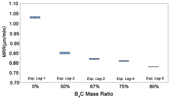
Figure 1.
SiC MRR of leg-1 to leg-5.
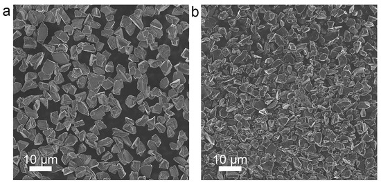
Figure 2.
SEM images of diamond (a) and B4C (b).
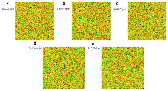
Figure 3.
Zygo images of leg-1 (a); leg-2 (b); leg-3 (c); leg-4 (d); leg-5 (e); Warmer colors (e.g., red, yellow) indicate higher regions, while cooler colors (e.g., blue, green) indicate lower regions on the SiC substrate surface.
Moreover, under equal process pressure, the powder sharpness reduction ratio of B4C is higher than that of diamond. When the B4C mass ratio is increased to 80 wt%, the TTV of post-lapping substrates reaches around 4 μm, which is significantly worse than the baseline performance. The surface roughness of the substrates showed only minor variations, decreasing with increasing B4C mass ratio (Figure 3 and Figure S4).
To evaluate the subsurface in silicon carbide (SiC) substrates induced by lapping with a hybrid abrasive slurry containing both diamond and boron carbide (B4C) particles, cross-sectional specimens were prepared using focused ion beam (FIB) milling and characterized by high-resolution scanning electron microscopy (HRSEM). Figure 4 presents cross-section SEM images of the post-lapping SiC substrates processed with leg-4 slurry. The cross-sectional SEM image (Figure 4d) shows that the hybrid abrasive lapping process produces a multi-modal damage layer. Within this layer, two distinct crack regimes can be identified: 1. Deep, vertically oriented cracks, typically extending 0.8–2.0 μm beneath the surface. These cracks exhibit characteristics similar to those induced by pure diamond abrasion, such as occasional branching propagation (Figure 4b and Figure S5a). They are attributed to the high-indentation stress imposed by the harder diamond particles during ploughing and cutting. 2. A shallower, dense network of micro-cracks and lateral cracks within the top 0.5 μm (Figure 4c and Figure S5b). This regime resembles the damage pattern from B4C lapping, featuring interconnected cracks that often run parallel to the surface. This morphology is likely caused by the shear-dominated micro-fracture and multi-point scratching facilitated by the smaller or fragmented B4C particles. Notably, interaction zones are observed where deep vertical cracks originating from diamond abrasion are intercepted or connected by the shallow lateral micro-cracks from B4C action (Figure 4d). This synergy suggests a sequential or simultaneous material removal mechanism: diamond particles may initiate deep fractures, while B4C particles subsequently promote material removal by linking and expanding these fracture networks near the surface. This combined effect might offer a balance between high lapping efficiency and controlled subsurface damage depth. However, the interconnected crack network poses a significant challenge for subsequent polishing, as it could lead to spalling or increased surface roughness if not adequately removed.
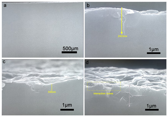
Figure 4.
Surface topography with lapped SiC wafer (a); Vertically oriented crack (b); Shallower micro-cracks (c); Interaction zones (d).
3.2. The Influence of Diamond and Boron Carbide Powder Size on Material Removal Rate and Roughness
To investigate the influence of different abrasive powder sizes on SiC removal rate and surface roughness, slurry formulations from leg-6 to leg-8 with a certain mass ratio but different diamond and B4C powder size was designed in Figure 5. Substrate lapped with leg-6 demonstrates better surface roughness (Sa) than baseline condition (72 nm), indicating that decreasing diamond powder size is beneficial in reducing substrate surface roughness since smaller diamond powder introduces shallower scratches at SiC. This improved roughness enhances the success rate of the polishing process, but using smaller diamond powder comes at the cost of a reduced removal rate, as evident by the fact that the removal rate with leg-6 is 0.59 μm/min, which is significantly lower than leg-4’s 0.81 μm/min.
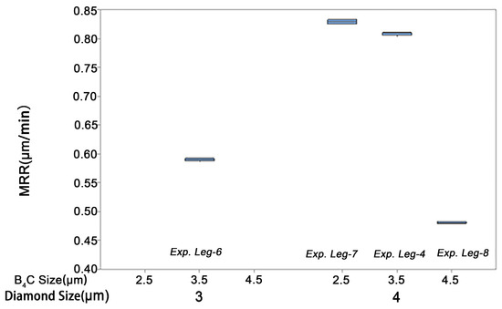
Figure 5.
MRR of leg-6 to leg-8.
Leg-7 maintains the same diamond size (4 μm) but a smaller B4C size (2.5 μm) when compared to leg-4. SiC removal rate is 0.83 μm/min with leg-7, which is even higher than leg-4. It is a fact that smaller-sized B4C does not suppress the diamond’s removal effect during the lapping process. Based on this mechanism, larger-sized B4C should have a lower SiC MRR. The test result of leg-8 (B4C size = 4.5 μm) matches this trend. SiC removal rate of leg-8 is 0.48 μm/min, much lower than those of leg-4 and leg-7. Surface roughness data from leg-4, leg-6, and leg-8 further reveal that the processes with a higher removal rate correlate with worse surface roughness.
Based on the comprehensive analysis of all experimental group data, we investigated the effects of four factors-diamond particle size, boron carbide particle size, boron carbide mass ratio, and the particle size difference between diamond and boron carbide—on two control indicators: the material removal rate and surface roughness of 8-inch silicon carbide substrates during lapping. As shown in Figure 6, when the diamond particle size exceeds that of boron carbide, the influence of particle size difference on the material removal rate tends to stabilize. This is attributed to the dominant role played by larger diamond particles in the lapping process. Once the diamond particle size exceeds that of boron carbide by more than 0.5 μm, the effect of further increasing the size difference on the removal rate of silicon carbide approaches saturation. Due to the polygonal morphology and superior self-sharpening characteristics of diamond abrasives, the particle size difference exhibits a significant influence on the surface roughness of the substrates. Smaller particles worsen implies that the mechanism for rougher surfaces is due to the use of smaller particles. In addition, the slurry is dominated by the larger diamond particles. When further increasing the size difference between diamond and boron carbide, it contributes little to the lapping rate but markedly worsens the surface roughness of the substrate. Based on these findings, maintaining the particle size difference between diamond and boron carbide at approximately 0.5 μm is considered the optimal choice.
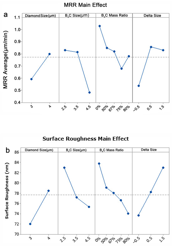
Figure 6.
MRR main effect of diamond size, B4C size, B4C mass ratio; delta Size (a); Surface roughness of diamond size, B4C size, B4C mass ratio; delta Size (b).
Figure 7 presents the interaction effect analysis of the other three factors, excluding the abrasive particle size difference. It can be observed that the surface roughness of the substrate decreases with an increase in the boron carbide content, with the improving trend slowing down after the boron carbide mass ratio exceeds 75%. Meanwhile, the material removal rate also decreases as the boron carbide content increases, primarily because the lapping action of diamond is restrained with the rising proportion of boron carbide. The particle sizes of boron carbide and diamond also exhibit notable effects on both the removal rate and substrate surface roughness. Under a fixed boron carbide content ratio, comparative analysis shows that the 3.5 μm boron carbide condition achieves a better balance between removal rate and surface roughness.
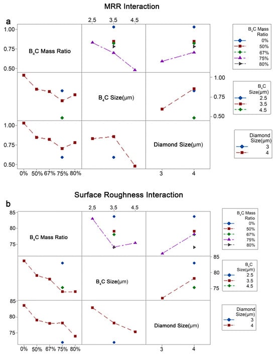
Figure 7.
MRR interaction of B4C mass ratio, B4C size, diamond size (a); Surface roughness interaction of B4C mass ratio, B4C size, diamond size (b).
Through this study, we have elucidated the mechanistic roles of diamond and boron carbide in the lapping process. While diamond serves as the primary component for material removal during the process, an appropriate proportion and particle size of boron carbide are essential to act as a buffer and polishing agent to ensure the surface roughness of the substrate after lapping. This approach enables an optimal balance between process efficiency and quality.
3.3. Subsurface Mechanical Damage Characterization
SSD can be detected using destructive and nondestructive methods. However, the accuracy and efficiency of destructive methods are relatively high. In this paper, inductively coupled plasma (ICP) etching technology was employed to detect and define the surface subsurface damage layer [15]. During the characterization, an inclined polishing method was applied. This process begins by creating an inclined interface that penetrates through the subsurface damage layer. The vertical height from the bottom of the subsurface damage layer to the material surface can be measured using a confocal laser scanning microscope (CLSM) and a 3D profilometer, allowing the thickness of the subsurface damage layer to be determined. This is an SSD-free material removal method [15]. The plasma diagnosis and etching behavior study showed its capability for fast material removal. Plasma flow simulation was used to optimize the etching position, and rapid SSD detection was finished within 2 min [15]. Figure 8a shows a top-view image of the inclined interface of leg-4 following ICP etching, captured using a confocal laser scanning microscope. The right portion depicts the unetched surface, which is uneven with pits, cracks, and scratches, whereas the left portion—the etched area—exhibits a flat and smooth surface. Figure 8b is a 3D microscope magnification diagram of the unetched area. Figure 8c,d is the cross-section profile along the yellow arrows in 8a, respectively. It can be observed that the signal-to-noise ratio is not stable from 0 to 250 μm on the horizontal axis. These unstable signals come from the roughness and the subsurface damage layer. In contrast, the signals from 0 to 125 μm are smooth, indicating that they come from an undamaged area. The subsurface damage layer depth can be ascertained by measuring the vertical distance from the last crack to the original rough surface. In this case, the lapping-induced subsurface damage layer measures 2.16 μm.
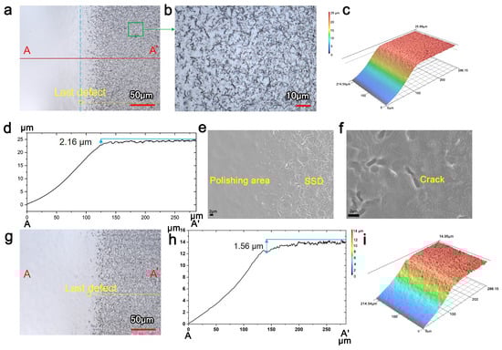
Figure 8.
The CLSM image of the etched slope of the leg-4 (a), amplification of damage zone (b), the cross-sectional profile of leg-4 along A–A′ (c,d), the SEM image of the etched slope of the leg-4 (e), the SSD SEM image of the leg-4 (f), the CLSM image of the etched slope of the leg-6 (g), the cross-sectional profile of leg-6 along A–A′ (h,i).
Since diamond powder size is a critical determinant for substrate surface roughness, subsurface damage in the substrates was also tested with varying diamond particle sizes. Figure 8g presents the data from the substrate lapped with slurry leg-6, which incorporates a smaller diamond powder size, revealing a subsurface damage layer depth of 1.56 μm. Comparing the subsurface damage layer depth of substrate lapped with leg-6 and leg-4, it can be observed that a smaller diamond powder size introduces a shallower subsurface damage layer. Precisely ascertaining subsurface damage depth is highly beneficial, as it guides slurry selection for the lapping process and determines the minimum polishing thickness in subsequent steps to effectively remove the lapping-induced damage layer.
A cross-sectional transmission electron microscopy (TEM) study was systematically conducted on a 4H-SiC single-crystal substrate following ICPE to reveal the microstructural characteristics of its surface and near-surface regions. Figure 9a–c shows the area of the unetched area of the SiC substrate. Cracks, stress, and amorphous layers can be clearly observed. However, in Figure 9d, high-resolution TEM (HRTEM) imaging clearly reveals an ultrathin (about 10 nm thick), continuous amorphous natural oxide layer at the outermost surface, and perfectly crystalline 4H-SiC was observed immediately below the interface, and the image corresponds to the face of 4H-SiC. EDX and mapping tests also show that the amorphous silicon carbide natural oxide layer is 10 nm. To ensure sample stability and prevent charge accumulation during Transmission Electron Microscopy (TEM) observation, a chromium oxide (CrO2) protective layer approximately 20 nm thick was deposited on the sample surface. This result proves that only a single crystal 4H-SiC remained on the crack-free surface formed by ICPE, and no new SSD was introduced. In addition, it further indicates that the ICPE process, under optimized conditions, selectively removes material without significantly altering the pre-existing subsurface damage features, making it an effective diagnostic technique for revealing the depth and morphology of the lapping-induced damaged layer [24]. The depth of the damage layer of the wafer after lapping is about 1–2 microns.
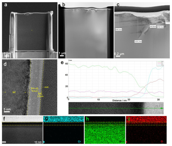
Figure 9.
TEM image of the unetched area of leg-4 (a–c), HRTEM image of etched area (d), EDX and mapping of the etched area (e–i).
3.4. Material Removal Mechanism
The lapping process using an iron plate and boron carbide (B4C)/diamond abrasives in a weakly alkaline environment (pH = 10) is, in essence, a dynamic, multi-field coupled mechanical–chemical–thermal refinement process. It performs exquisitely precise operations at the micro-scale, which can be broken down into four highly synergistic, cyclical stages, as illustrated in Figure 10.
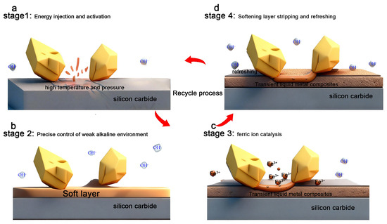
Figure 10.
Material removal mechanism of the lapping process (a–d).
- Stage 1: energy injection and reactor initiation.
First, the core of this stage is the conversion of macroscopic mechanical energy into the activation energy that drives microscopic chemical reactions. Under the external load, a sharp diamond abrasive grain is pressed into the SiC surface. Due to the nanoscale contact area, the local pressure instantaneously exceeds several GPa. This high pressure is sufficient to initiate dislocation multiplication and slip within the SiC crystal lattice, directly causing the stretching, distortion, and even breaking of chemical bonds, lowering the energy barrier for subsequent chemical reactions [25,26,27,28].
Then, the “hot spot” micro-reactor is the origin. The relative motion between the lapping plate and the substrates causes the abrasive grain to slide across the surface at high speed. Vast amounts of kinetic energy are converted into heat via friction almost instantaneously. Because the interaction time is extremely short (on the order of microseconds), the heat has no time to diffuse, resulting in the formation of a confined, transient micro-scale, high-temperature, high-pressure “reactor” at the leading edge of the abrasive grain [29,30]. This heat can be used to activate the surface of silicon carbide [31]. Under the combined influence of stress and heat, the Si-C covalent bonds in the outermost layer break, destroying the crystal structure and forming an amorphous, active layer rich in dangling bonds. Similarly, atoms from the surface of the iron plate are “scraped off” and subjected to mechanical action, forming nanoscale, fresh iron debris with clean, highly active surfaces.
- Stage 2: precise interface regulation in a weakly alkaline environment.
The weakly alkaline environment (pH = 8–11) acts here as a “reaction moderator” rather than a “strong etchant.” OH− ions from the weakly alkaline solution adsorb onto the already activated SiC surface. They act as catalysts, significantly lowering the activation energy for the reaction between SiC and water or atmospheric oxygen. The SiC surface is oxidized, such as SiC + 2O2 + 2H2O + OH−→SiO2 + CO2 + 2H2. What forms is not pure SiO2, but a soft, easily sheared siliceous hydrated gel layer. For the silicon layer, the weakly alkaline environment dissolves this siliceous gel at a moderate, controlled rate, forming soluble silicates (SiO2 + 2NaOH→ Na2SiO3 + H2O) [32]. This rate ensures that the softened layer does not build up excessively (causing loading), while also preventing it from being dissolved too quickly, which would re-expose the pristine, hard, and brittle SiC. However, for the iron plate, the weakly alkaline environment promotes the formation of a thin, dense γ-Fe2O3/Fe3O4 passivation film on the iron surface [33]. This film prevents rapid corrosion of the lapping plate on a macroscopic scale. However, within the microscopic “hot spot” reactor, the immense mechanical stress can instantaneously rupture it locally, exposing the underlying active iron atoms to participate in the reaction. This achieves an exquisite balance of “macroscopic protection, microscopic supply.”
- Stage 3: Iron-catalyzed transient liquid phase reaction.
This is the climax and core of the entire mechanism. Within the “hot spot” reactor, iron transitions from a solid participant to a liquid catalyst. The active iron debris from the lapping plate encounters silicon from the decomposed SiC, boron from the decomposed B4C abrasive, and environmental carbon. At temperatures far below their individual melting points (e.g., Fe-B eutectic point ~1174 °C, Fe-Si ~1200 °C), they instantaneously form an ultra-thin, nanoscale film of liquid alloy [34]. This liquid film becomes a superhighway for atomic diffusion. Silicon and carbon rapidly dissolve into the liquid phase from the disrupted SiC surface. Boron diffuses in from the B4C abrasive grain. They collide and react at high speed with iron atoms within the liquid phase, forming iron silicides, borides, and carbides. In addition, the final result is the formation, on top of the original hard SiC, of a nanometer-thick composite softened layer consisting of intermetallic compounds, amorphous carbon, and residual siliceous gel. The shear strength and hardness of this layer are orders of magnitude lower than those of the SiC substrate, which is the basis for the final stage.
- Stage 4: Precise delamination of the softened layer and system refresh.
The goal of this stage is to remove this softened layer from the substrate with minimal damage. As the trailing edge of the abrasive grain passes over this softened region, it no longer requires immense force to initiate brittle fracture. The abrasive grain needs to apply a relatively small shear force to peel up the entire softened material layer and remove it as chips or scraps. This constitutes a “quasi-plastic” or “ductile regime” material removal mode, effectively preventing cracks from propagating into the substrate. Then, the weakly alkaline lapping fluid swiftly flushes away this reaction debris (rich in Fe, Si, B, and C), updating the machining zone and preventing it from participating in secondary reactions or scratching the surface. A fresh, new SiC surface is exposed, immediately entering the next cycle. The lapping plate rotates, bringing a new source of iron. In addition, the abrasive grains self-sharpen, exposing new sharp edges, which is a self-optimizing refinement loop. Mechanical energy creates the extreme physical conditions (high temperature, high pressure) and active surfaces required for the reactions [35,36]. Weakly alkaline chemistry provides a controlled reaction environment, promoting beneficial surface softening while suppressing harmful over-corrosion and equipment wear. Meanwhile, the iron lapping plate acts as a sustainable catalyst source, enabling a fundamental shift from fracturing to delamination through the transient liquid phase reaction. This process is not simple abrasion, but a refinement process-a cycle of “activation-catalysis-transformation-delamination” occurring millions of times per second within countless microscopic reactors. It uses the most ingenious physicochemical methods to transform the challenge of machining an ultra-hard material into the simpler task of handling one soft reacted layer after another, thereby achieving the perfect trifecta of high efficiency, low damage, and superior surface quality.
3.5. Lapping in the SiC Process Chain
In the conventional silicon carbide (SiC) processing route (slicing → grinding → polishing), the lapping process can effectively replace the conventional grinding step. Dual-side lapping provides more uniform material removal and stress release across the wafer due to balanced mechanical forces applied simultaneously to both surfaces. This leads to superior global flatness and reduced subsurface stress gradients compared to single-side grinding. The surface quality (morphology and roughness) generated at this lapping stage is critically upstream of the final polishing. If the lapped surface exhibits poor flatness or abnormally high roughness, this creates an uneven starting point for the subsequent chemical-mechanical polishing (CMP). Consequently, the CMP process must remove a non-uniform amount of material to achieve a planar surface, often resulting in an increased TTV of the polished wafer [37,38,39]. Furthermore, a poorly prepared lapped surface typically contains a higher density of microscratches and defects, which can propagate or be only partially removed during polishing, leading to a higher count of surface scratches in the final polished substrate. Most critically, the depth of the subsurface damage layer (SSD) remaining after final polishing has a direct impact on epitaxial film quality. If the polishing step does not fully remove the damage from previous stages, or if it introduces its own deeper SSD, this defective layer acts as a nucleation site for crystallographic defects during subsequent epitaxial growth. Therefore, a deeper residual SSD in the polished substrate directly correlates with an increased density of defects (e.g., dislocations, stacking faults) in the epitaxial SiC film, ultimately degrading the performance and yield of fabricated electronic devices.
4. Conclusions
This study systematically investigated the effects of diamond and boron carbide (B4C) mixed abrasives on the lapping performance of 4H-SiC substrates. The main conclusions are as follows:
- The abrasive mixing ratio is key to balancing efficiency and quality. Increasing the proportion of B4C effectively improves surface roughness. However, exceeding 75 wt% leads to a significant decrease in the material removal rate (MRR) and worse total thickness variation (TTV).
- Abrasive particle size governs the depth of subsurface damage. Larger diamond particles increase the MRR but exacerbate subsurface damage (SSD). Smaller B4C particles (e.g., 2.5 μm) help maintain a higher MRR while contributing to worse surface quality.
- Optimal processing parameters are recommended. To achieve a balance between efficiency and surface integrity, a slurry formulation with a diamond-to-B4C mass ratio of approximately 1:3 (i.e., 75 wt.% B4C) and a particle size difference of about 0.5 μm is proposed.
This work elucidates the synergistic material removal mechanism involving mechanical–chemical–thermal coupling in a weakly alkaline environment, providing both theoretical insight and practical guidance for the efficient and low-damage lapping of 4H-SiC substrates.
Supplementary Materials
The following supporting information can be downloaded at: https://www.mdpi.com/article/10.3390/cryst16020142/s1, Figure S1: Double-sided lapping machine equipment photo; Figure S2: Tropel image of the SiC substrate after lapping process; Figure S3: Photo of the SiC lapped substrate; Figure S4: Surface roughness Sa of Leg-1 to Leg-5; Figure S5: SEM image of lapped susbstrate of pure diamond (a), B4C(b).
Author Contributions
X.S.: Conceptualization, Data curation, Formal analysis, Investigation, and Writing—original draft; D.W.Z.: Supervision, Writing—review and editing, and Resources; L.Z.: Supervision and Writing—review and editing. All authors have read and agreed to the published version of the manuscript.
Funding
This work was financially supported by Fudan University and SICC Co., Ltd., Shanghai.
Data Availability Statement
The original contributions presented in this study are included in the article. Further inquiries can be directed to the corresponding author.
Acknowledgments
Deepseek-V4 was used during the preparation of this manuscript for language polishing.
Conflicts of Interest
Xiaoming Sui and Lin Zhang were employed by SICC Co., Ltd. The remaining authors declare that the research was conducted in the absence of any commercial or financial relationships that could be construed as potential conflicts of interest.
References
- Ma, G.; Li, S.; Liu, F.; Zhang, C.; Jia, Z.; Yin, X. A review on precision polishing technology of single-crystal SiC. Crystals 2022, 12, 101. [Google Scholar] [CrossRef]
- Yu, Y.; Hu, Z.; Wang, W.; Zhao, H.; Lu, J.; Xu, X. The double-side lapping of SiC wafers with semifixed abrasives and resin–combined plates. Int. J. Adv. Manuf. Technol. 2020, 108, 997–1006. [Google Scholar]
- Guo, F.; Shao, C.; Chen, X.; Xie, X.; Yang, X.L. Shape modulation due to sub-surface damage difference on N-type 4H–SiC wafer during lapping and polishing. Mater. Sci. Semicond. Process. 2022, 152, 107124. [Google Scholar] [CrossRef]
- Shi, D.; Zhao, T.C.; Ma, T.F.; Pan, J.P. Study on improving the precise machinability of single crystal SiC by an ultrasonic-assisted hybrid process. Materials 2021, 14, 7320. [Google Scholar] [CrossRef]
- Luo, Q.F.; Lu, J.; Tian, Z.G.; Feng, J. Controllable material removal behavior of 6H-SiC wafer in nanoscale polishing. Appl. Surf. Sci. 2021, 562, 150219. [Google Scholar] [CrossRef]
- Zhang, Z.S.; Cai, H.; Gan, D.; Hu, W.; Yang, J.; Liu, X.; Guo, Y.; Guo, L.; Wang, W.; Chen, X. A new method to characterize underlying scratches on SiC wafers. CrystEngComm 2019, 21, 1200–1204. [Google Scholar] [CrossRef]
- Yin, T.; Doi, T.; Kurokawa, S.; Zhou, Z.; Feng, K.P. Polishing characteristics of MnO2 polishing slurry on the si-face of SiC wafer. Int. J. Precis. Eng. Manuf. 2018, 19, 1773–1780. [Google Scholar] [CrossRef]
- Ji, P.X.; Zhang, K.M.; Zhang, Z.Z.; Zhao, M.; Li, R.; Hao, D.; Moro, R.; Ma, Y.; Ma, L. A general strategy for polishing SiC wafers to atomic smoothness with arbitrary facets. Mater. Sci. Semicond. Process. 2022, 144, 106628. [Google Scholar] [CrossRef]
- Lu, J.; Xu, Y.C.; Zhang, Y.H.; Xu, X.P. The effects of SiO2 coating on diamond abrasives in sol-gel tool for SiC substrate polishing. Diam. Relat. Mater. 2017, 76, 123–131. [Google Scholar] [CrossRef]
- He, Z.B.; Huang, H.; Yin, F.; Xu, X.P. Development of a brazed diamond wire for slicing single-crystal SiC ingots. Int. J. Adv. Manuf. Technol. 2017, 91, 189–199. [Google Scholar] [CrossRef]
- Gao, Y.F.; Chen, Y. Sawing stress of SiC single crystal with void defect in diamond wire saw slicing. Int. J. Adv. Manuf. Technol. 2019, 103, 1019–1031. [Google Scholar] [CrossRef]
- Gao, Y.F.; Chen, Y.; Ge, P.Q.; Zhang, L.; Bi, W. Study on the subsurface microcrack damage depth in electroplated diamond wire saw slicing SiC crystal. Ceram. Int. 2018, 44, 22927–22934. [Google Scholar] [CrossRef]
- Zhang, Y.L.; Xie, X.Z.; Huang, Y.A.; Hu, W.; Long, J.Y. Internal modified structure of silicon carbide prepared by ultrafast laser for wafer slicing. Ceram. Int. 2023, 49, 5249–5260. [Google Scholar] [CrossRef]
- Zhang, Y.; Zhang, L.F.; Chen, K.Y.; Liu, D.; Lu, D.; Deng, H. Rapid subsurface damage detection of SiC using inductivity coupled plasma. Int. J. Extrem. Manuf. 2021, 3, 035202. [Google Scholar] [CrossRef]
- Zhao, S.; Chen, Z.M.; Pan, P.; Wang, H.H. Oriented Lapping of SiC Wafers. J. Synth. Cryst. 2010, 39, 366–368. [Google Scholar]
- Zhang, X.; Zhu, R.Z.; Zhang, X.Q.; Wang, M.; Pi, X. Influence of abrasive morphology and dispersion medium on lapping quality of 4H-SiC wafers. J. Synth. Cryst. 2023, 52, 49–55. [Google Scholar]
- Pan, J.S.; Yan, Q.S.; Li, W. Analysis on surface performance of 6H-SiC monocrystalline wafer with single-sided lapping method. Diam. Abras. Eng. 2014, 34, 2–6. [Google Scholar]
- Tsai, M.-Y.; Li, K.-Y.; Ji, S.-Y. Novel abrasive-impregnated pads and diamond plates for the grinding and lapping of single-crystal silicon carbide wafers. Appl. Sci. 2021, 11, 1783. [Google Scholar] [CrossRef]
- Guo, Y.J.; Jing, L.; Xu, L. Tribochemical action on the tribochemical mechanical lapping (0001) C plane of the SiC single-crystal substrate. Int. J. Mod. Phys. B 2022, 36, 2240027. [Google Scholar]
- Zhang, X.; Liu, X.; Wang, Y.; Zhu, R.; Zhang, X.; Zhang, Y.; Wang, R.; Yang, D.; Pi, X.D. Optimizing the flatness of 4H-silicon carbide wafers by tuning the sequence of lapping. Semicond. Sci. Technol. 2023, 3, 034001. [Google Scholar] [CrossRef]
- Fang, L.; Xiao, Y.; Yan, G.; Ao, Z.; Yang, M. Surface prediction and experimental study of single crystal SiC fixed abrasive lapping. Laser Optoelectron. Prog. 2025, 21, 2116002. [Google Scholar]
- Chen, J.P.; Zhu, Y.W.; Wang, J.B.; Peng, Y.; Yao, J.; Ming, S. Relationship between mechanical properties and processing performance of agglomerated diamond abrasive compared with single diamond abrasive. Diam. Relat. Mater. 2019, 100, 107595. [Google Scholar] [CrossRef]
- Yin, J.; Bai, Q.; Zhang, B. Methods for detection of subsurface damage: A review. Chin. J. Mech. Eng. 2018, 31, 41. [Google Scholar] [CrossRef]
- Liu, L.L.; Zhao, Z.Y.; Zhang, S.T.; Yu, T.; Yang, G. Tetragonal structure BC4 as a superhard material. J. Phys. Chem. C 2017, 121, 10119–10123. [Google Scholar] [CrossRef]
- Geng, W.H.; Yang, G.; Zhang, X.Q.; Zhang, X.; Wang, Y.; Song, L.; Chen, P.; Zhang, Y.; Pi, X.; Yang, D.; et al. Identification of subsurface damage of 4H-SiC wafers by combining photo-chemical etching and molten-alkali etching. J. Semicond. 2022, 43, 102801. [Google Scholar] [CrossRef]
- Li, H.H.; Cui, C.C.; Lu, J. Mueller matrix ellipsometric characterization of nanoscale subsurface damage of 4H-SiC wafers: From grinding to CMP. Front. Phys. 2021, 9, 820637. [Google Scholar] [CrossRef]
- Yan, Q.S.; Chen, S.K.; Pan, J.S. Surface and subsurface damage characteristics and material removal mechanism in 6H-SiC wafer grinding. Mater. Res. Innov. 2014, 18, 742–746. [Google Scholar] [CrossRef]
- Zhou, Y.; Huang, Y.; Li, J.; Zhu, F.Z. The effect of contact types on SiC polishing process. Mater. Sci. Semicond. Process. 2022, 147, 106709. [Google Scholar] [CrossRef]
- Malkin, S.; Guo, C. Thermal analysis of grinding. Ann. CIRP 2007, 56, 760–782. [Google Scholar] [CrossRef]
- Huang, Y.; Zhou, Y. Understanding of the effect of wear particles removal from the surface on grinding silicon carbide by molecular dynamics simulations. Diam. Relat. Mater. 2023, 137, 110150. [Google Scholar] [CrossRef]
- Daviau, K.; Lee, K. High-pressure, high-temperature behavior of silicon carbide: A review. Crystals 2018, 8, 217. [Google Scholar] [CrossRef]
- Friedrichs, P.; Burte, E.P.; Schörner, R. Interface properties of metal-oxide-semiconductor structures on n-type 6H and 4H-SiC. J. Appl. Phys. 1996, 79, 7814–7819. [Google Scholar] [CrossRef]
- He, J.; Zhang, H.; Chen, J.; Liu, Y.; Wang, J.; Yao, F. Mechanistic study of the effect of Fe on the oxidation behavior of FeCoCrNi high-entropy alloys in high-temperature steam. J. Phys. Conf. Ser. 2025, 3013, 012017. [Google Scholar] [CrossRef]
- Hauffe, K. The mechanism of oxidation of metals and alloys at high temperatures. Prog. Met. Phys. 1953, 4, 71–104. [Google Scholar] [CrossRef]
- Lu, K.; Lu, J. Nanostructured surface layer on metallic materials induced by surface mechanical attrition treatment. Mater. Sci. Eng. A 2004, 375–377, 38–45. [Google Scholar] [CrossRef]
- Meng, B.; Zhang, Y.; Zhang, F. Material removal mechanism of 6H-SiC studied by nano-scratching with Berkovich indenter. Appl. Phys. A 2016, 122, 247. [Google Scholar] [CrossRef]
- Chen, X.; Pan, J.; Zhang, H.; Liu, Y. Synthesis of CeO2 composite particles for chemical mechanical polishing of single-crystal SiC substrates and their polishing applications: A review. Appl. Mater. Interfaces 2026, 18, 4685–4700. [Google Scholar] [CrossRef]
- Je, H.; Kang, S.; Kim, S. Challenges and innovations in chemical mechanical polishing in the more-than-moore era. Int. J. Precis. Eng. Manuf.-Green Technol. 2026. [Google Scholar] [CrossRef]
- Li, A.; Zhou, J.; Niu, X.; Liu, Z.; Ma, Q.; Song, S.; Wang, M.; Hu, B. Advances and challenges in chemical mechanical polishing of silicon carbide: Materials, mechanisms, and future directions. J. Mater. Chem. C 2025, 13, 22921–22952. [Google Scholar] [CrossRef]


Disclaimer/Publisher’s Note: The statements, opinions and data contained in all publications are solely those of the individual author(s) and contributor(s) and not of MDPI and/or the editor(s). MDPI and/or the editor(s) disclaim responsibility for any injury to people or property resulting from any ideas, methods, instructions or products referred to in the content. |
© 2026 by the authors. Licensee MDPI, Basel, Switzerland. This article is an open access article distributed under the terms and conditions of the Creative Commons Attribution (CC BY) license.