Abstract
This work presents a study of copper selenite nanocrystals, obtained for the first time by chemical deposition (template synthesis) in a SiO2/Si track template, and investigates their properties. The obtained nanostructures were subjected to structural, optical, and electrical analysis. After deposition, X-ray diffraction (XRD) analysis confirmed the formation of the orthorhombic phase CuSeO3. Subsequent annealing in a vacuum at 800 °C and 1000 °C led to successive phase transformations: to the monoclinic phase and, finally, to the triclinic polymorph of copper selenite. Photoluminescence (PL) analysis showed that the intensity and spectral position of the emission peaks vary depending on the crystal structure, which is associated with changes in defects and bandgap width as a result of heat treatment. Current–voltage characteristic (CVC) measurements showed that the phase composition significantly affects electrical conductivity. In particular, the transition to the triclinic phase after annealing at 1000 °C led to noticeable changes in optical and electrical properties compared to the initial material. Thus, a direct relationship has been established between heat treatment conditions, crystal structure, and functional properties of CuSeO3-based materials, opening up possibilities for their application in photonics and electronics.
1. Introduction
Copper chalcogenide- and oxysalt-based compounds are of considerable interest in materials science due to their exceptional optical, electronic, and catalytic properties, which are determined by their diverse structural chemistry and tunable electronic configurations [1]. CuSeO3 is a promising copper compound belonging to the class of chalcogenides and exhibits significant potential in various fields. In particular, it can be used in catalysis [2], serve as a silicon substitute in solar cells [3,4], be applied in batteries and supercapacitors [5], and act as an anode material in lithium-ion batteries [6]. Moreover, CuSeO3 also finds applications in environmental protection tasks [7].
Given these areas of application, the synthesis of CuSeO3 nanostructures represents an important step toward utilizing their properties for various purposes. Several methods for producing copper selenite have been developed, including hydrothermal synthesis [8,9], the chemical vapor transport method [10,11], and spray pyrolysis complemented by selenization and partial oxidation [6]. However, the fabrication of nanostructured copper selenite with well-defined and reproducible dimensions remains an insufficiently explored area.
In the present study, a template synthesis method is employed to address this issue, providing precise control over the size of the resulting nanostructures. A SiO2/Si template produced via ion implantation will serve as the basis for creating a structure with the desired properties. Initially, SiO2/Si structures will be irradiated with high-energy heavy ion beams and subsequently chemically etched using specialized solutions to form nanopores. These pores will then be filled with various materials. The use of this template-based approach has already led to the development of unique composite materials [12,13,14,15,16] with promising characteristics for various practical applications.
The practical applicability of these materials is directly related to the ability to control their defects, phase composition and structure. Thermal annealing is one of the most effective ways to achieve such control. However, despite the growing interest in copper selenides, systematic studies of their properties after heat treatment remain insufficiently explored. There is a particularly acute lack of data on the behavior of CuSeO3 at high temperatures (800–1000 °C). This is important because for related oxide systems [17] and copper-based materials [18], it is precisely this temperature range that critically affects recrystallisation, changes in copper valence and oxygen vacancy concentration, which radically changes their functional characteristics.
The aim of this study is to obtain copper selenite (CuSeO3) nanocrystals using a template synthesis method, which involves chemical deposition in SiO2/Si track templates, followed by studying the effect of high-temperature annealing (at 800 °C and 1000 °C) on the phase composition, optical and electrophysical properties of the obtained nanostructures.
2. Materials and Methods
2.1. Synthesis of CuSeO3 Nanocrystals
Copper selenite (CuSeO3) nanocrystals were synthesized by chemical deposition using SiO2/Si templates. The work uses Si (100) plates in the form of disks with a diameter of 10 cm and a thickness of 500 μm. For p-type Si, boron is added at a concentration of 1 ppm. An oxide layer approximately 530 nm thick was thermally grown on a silicon substrate (Si (100)) at 900 °C in a humid atmosphere. To fabricate the SiO2/Si structure, the samples were irradiated with Xe ions to create latent tracks in the SiO2 layer. To form nanopores, the samples were treated with a 4% aqueous hydrofluoric acid (HF) solution for 5–7 min at room temperature. The resulting nanochannels were then filled using the chemical deposition (CD) method [15]. Before deposition, the substrates were thoroughly cleaned in an ultrasonic cleaner to remove various impurities.
The chemical deposition solution was prepared by dissolving copper (II) chloride dihydrate (CuCl2·2H2O, Sigma-Aldrich, St. Louis, USA) and selenium dioxide (SeO2, Alfa Aesar, Ward Hill, USA) in deionized water (resistivity 18.2 MΩ·cm) at concentrations of 0.1 M and 0.1 M, respectively, to maintain a stoichiometric Cu:Se ratio of 1:1. The mixture was stirred with a magnetic stirrer for 5 min at room temperature (18 ± 2 °C) until a clear, homogeneous solution was obtained. The cleaned SiO2/Si templates were then immersed in the reaction solution. Deposition was carried out for 20, 40, and 60 min. Afterward, the samples were removed, thoroughly rinsed with deionized water to eliminate weakly attached salts, and dried at room temperature.
2.2. Characterization Methods
The morphological features of the synthesized nanostructures were examined using a dual-beam scanning electron microscope Zeiss Crossbeam 540 (Jena, Germany) at an accelerating voltage of 1–3 kV, using InLens and SE detectors to enhance surface contrast and visualize the internal pore structure, and mounted onto aluminum stubs using carbon conductive tape.
The crystalline structure and phase purity of the nanostructures were determined by X-ray diffraction (XRD) using a Rigaku SmartLab diffractometer (Rigaku, Tokyo, Japan) with a high-energy resolving 2D detector HPAD HyPix3000 (Rigaku, Tokyo, Japan) in the 2θ range from 40 to 70° at a voltage of 40 kV. TOPAS 4.2 software and the ICDD international database (PDF-2 Release 2020 RDB) were used to analyze the diffraction patterns and determine the phase composition and unit cell parameters of the substances.
To investigate the optical properties and defect states, photoluminescence (PL) spectroscopy was performed at room temperature. The spectra were obtained using a CM2203 spectrofluorimeter (Solar, Minsk, Belarus). PL spectra were recorded in the wavelength range from 400 nm to 800 nm at room temperature. The use of two double monochromators ensured minimal interference, guaranteeing high measurement accuracy.
The electrical properties were evaluated by current–voltage (CVC) measurements using a VersaSTAT 3 system (Ametek, Berwyn, PA, USA). Current and voltage characteristics were measured on an array of filled nanochannels with an area of 0.3 cm2.
The heat treatment of the synthesized samples was carried out in a vacuum at 800 and 1000 °C for 60 min using an AVERON furnace (Yekaterinburg, Russia). The heating rate was 30 °C/min.
3. Results and Discussion
3.1. SEM and XRD
Figure 1 presents SEM images of silicon nanopores filled with copper selenite via a chemical deposition process conducted for 20, 40, and 60 min at room temperature.
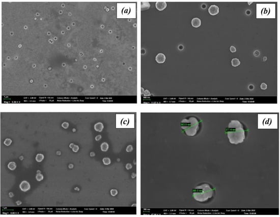
Figure 1.
SEM images of the nanoprecipitates obtained after chemical deposition for three different deposition durations: (a) 20 min, (b) 40 min, (c) 60 min and (d) nanopores with dimensions.
The average nanopore diameter was 375 nm (Figure 1d). The deposition time directly influences the degree of pore filling. After 20 min, the initial filling of the pores with small nanocrystals is observed (Figure 1a); at 40 min, the filling becomes more substantial (Figure 1b); and after 60 min, the pores are almost completely filled (Figure 1c), accompanied by the emergence of crystallite outgrowths on the surface.
Analysis of the deposited sample structures revealed that the nanoprecipitates formed within the SiO2/Si template correspond to CuSeO3 with an orthorhombic crystal structure (ICDD PDF-2 card No. 01-072-4732) and space group Pnma (62), as confirmed by X-ray diffraction analysis.
The results of the study on copper selenite nanocrystals within the SiO2/Si template, including their crystallographic parameters and X-ray diffraction patterns, are presented in Table 1 and Figure 2.

Table 1.
Crystallographic parameters of the as-deposited nanocrystals.
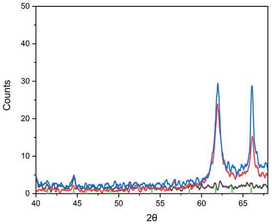
Figure 2.
XRD patterns of the deposited nanocrystals for three different deposition durations (black line—20 min, red line—40 min and blue line—60 min, green line—the CuSeO3 reference pattern).
As seen in Figure 2, with increasing deposition time, the deposited material has more time to grow and form well-defined crystalline structures, resulting in stronger and sharper XRD peaks.
3.2. Computer Modeling of CuSeO3
We also performed non-empirical calculations of the CuSeO3 crystal. Calculations that were performed in this work used the global hybrid functional B3LYP [19] and LCAO basis set approach [20,21] as implemented in the CRYSTAL program [22]. The all-electron Gaussian-type basis sets (pob_DZVP_rev2) for Cu, Se and O atoms were taken from CRYSTAL basis set database [22]. The total energy convergence threshold for the self-consistent field (SCF) and structure optimization procedure was chosen at 10-7 Hartree. For the optimization procedure, the quasi-Newton scheme was used. Gradients are estimated every time the total energy is computed; the second derivative matrix (i.e., Hessian matrix) is accordingly constructed from the gradients and updated by BFGS algorithm [22]. Optimization is considered complete when the change in energy between steps is below 10-7 a.u. and the default gradient and displacement criteria are satisfied. The effective atomic charges, as always, were determined using the Mulliken population analysis [23]. The integration of the reciprocal space was performed with a Pack-Monkhorst 8 × 8 grid [24], resulting in 125 k-points.
We used a periodic model of a primitive CuSeO3 cell, consisting of 20 atoms. The calculated lattice parameters (a, b, c), crystal density (ρV), and effective atomic charges (qeff) are presented in Table 2 together with our experimental results.

Table 2.
Bulk characteristics of pure CuSeO3 as calculated by means of the DFT-LCAO method in this study.
The calculated density of states and corresponding band structure of CuSeO3 are shown in Figure 3. The valence band is partially filled and has some empty bands above the Fermi level. It consists mainly of cationic Cu d states and anionic O 2p states, while the conduction band consists of O and Se p-orbitals. These states hybridize in the valence band and in the conduction band, respectively. Thus, there is no direct hybridisation of Cu-d and Se-p orbitals, which is also reflected in the crystal structure of CuSeO3.
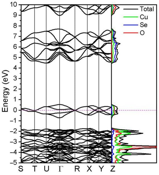
Figure 3.
Density of states and band structure of pure CuSeO3 crystal. The horizontal dashed line indicates the Fermi level.
For many transition metal oxides containing ions with partly filled d orbitals DFT predicts metallic states as opposed to experimentally found insulating states. However, we found an indirect band gap of 3.97 eV that close to the experimentally observed 3.9 eV [9]. The valence band maximum (VBM) is located at the Г-point (empty state), while the conduction band minimum (CBM) lies near the U-point in reciprocal space. The obtained results of CuSeO3 are in good agreement with other previous studies that used the projector augmented wave (PAW) approach [9].
Good agreement of the calculated electronic and structural properties with the experimental data gives confidence in the correct prediction of the formation energies of intrinsic point defects, which often are not achievable from pure DFT methods due to well-known band gap errors.
3.3. Photoluminescence
The photoluminescence of CuSeO3-NCs/SiO2/Si was investigated in the spectral range of 400–600 nm under excitation with a wavelength of λ = 250 nm. Figure 4 shows the photoluminescence spectrum of the CuSeO3-NCs/SiO2/Si structures.
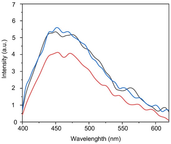
Figure 4.
PL spectrum of the as-deposited nanocrystals for three different deposition durations (black line—20 min, red line—40 min and blue line—60 min).
The photoluminescence spectra of CuSeO3 nanocrystals exhibit a single broad emission band, indicating the presence of an amorphous structure and a high density of defect states. The emission at 440 nm observed in the CuSeO3 structure can be attributed to near-band-edge or excitonic transitions, as observed in other copper oxide systems [25]. The peaks in the 450–475 nm range are associated with transitions originating from shallow defects. These transitions are often interpreted as donor–acceptor pair recombinations involving shallow defect levels. Among these defects, copper vacancies can be identified. Copper vacancies create tail states within the band gap, thereby increasing hole concentration and promoting more efficient charge separation and transfer, thus influencing the emission characteristics [26]. Shallow defects may also include the presence of oxygen interstitials and copper vacancies [27]. The peak at 562 nm, which is more pronounced in the sample deposited for 20 min, is associated with oxygen vacancy complexes or specific copper vacancy configurations [28,29]. The disappearance of this peak with increasing deposition time indicates that it represents an immature defect structure that is eliminated during prolonged growth. The shift and narrowing of the emission peaks (from 475 nm to 468 nm) with increasing deposition time indicate a reduction in deep defect states and an improvement in crystalline quality, which is consistent with observations in other metal oxide–based semiconductor systems [30].
3.4. Current–Voltage Characteristics
Measurements of the current–voltage characteristics provide a clear understanding of the mechanisms of charge transfer.
The current–voltage characteristics (CVC) after deposition (Figure 5) clearly show a nonlinear dependence of current on voltage (I(U)), which manifests itself in the form of diode behavior. When positive potentials are applied, a significant jump in current is observed, reaching values of about 1.6 mA. This asymmetry in the characteristics indicates the presence of barrier transitions and a low degree of order in the crystal structure. X-ray diffraction (XRD) data confirm this, showing the presence of an amorphous origin and diffraction peaks corresponding to the orthorhombic phase of CuSeO3. In this state, the conductivity of the material is predominantly surface-based, highly sensitive to defects, and the main mechanism of charge transfer is grain boundary current [31].
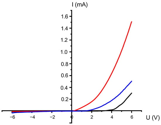
Figure 5.
Current–voltage characteristics of nanocrystals after CD for three different deposition durations (black line—20 min, red line—40 min and blue line—60 min).
3.5. Impact of Thermal Annealing on Structural and Optoelectronic Properties
To improve crystallinity and evaluate the thermal stability of the created nanostructures, the samples were thermally treated at high temperatures.
Figure 6 and Table 3 show the crystallographic parameters and the diffractograms of nanocrystals after thermal annealing at 800 °C.
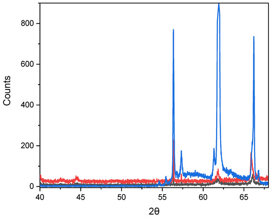
Figure 6.
Diffraction patterns of X-rays from nanocrystals after annealing at 800 °C for three different deposition durations (black line—20 min, red line—40 min and blue line—60 min).

Table 3.
Crystallographic parameters of the nanoprecipitates after 800 °C annealing.
After heat treatment at 800 °C, a significant change in the diffraction pattern (Figure 6) is observed.
Heat treatment at 800 °C leads to the complete formation of the monoclinic phase (especially for the blue curve) CuSe2O5 (JCPDS No. 00-047-1745), accompanied by an increase in crystallite size and a decrease in microdeformations of the crystal lattice. According to the studies [32,33], this phase is thermodynamically stable in the range of 600–850 °C.
A significant increase in the intensity of the main peaks (for the blue curve) indicates an increase in the degree of crystallinity and the formation of an ordered phase after high-temperature annealing.
In contrast, the black and red curves show broader and less intense peaks, which correspond to the partially amorphous state of the samples.
After annealing at 1000 °C (Figure 7), the intensity of the diffraction lines decreases significantly, indicating partial amorphization or degradation of the crystal structure. X-ray structural analysis showed that the peaks correspond to the triclinic phase CuSeO3 (P-1). The appearance of triclinic CuSeO3, despite the initial orthorhombic phase, is associated with high-temperature reduction in selenite after decomposition of CuSe2O5.
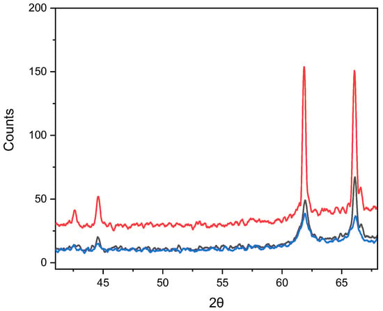
Figure 7.
Diffraction patterns of X-rays from nanocrystals after annealing at 1000 °C for three different deposition durations (black line—20 min, red line—40 min and blue line—60 min).
Figure 7 and Table 4 show the crystallographic parameters and the diffractograms of nanocrystals after thermal annealing at 1000 °C.

Table 4.
Crystallographic parameters of the nanoprecipitates after 1000 °C annealing.
The triclinic form of CuSeO3, as established in the work [34], becomes stable at high temperatures and in the deficiency of selenium dioxide (SeO2). Its structure is characterized by distortions and non-equivalence of Cu–O and Se–O bonds. This transition from an orthorhombic to a triclinic structure, accompanied by a decrease in symmetry, is a typical consequence of degassing of systems containing volatile anions during rapid cooling. The observed thermal behavior is confirmed by data for oxyselenates of other transition metals, which also decompose at high temperatures [35].
The photoluminescence (PL) spectra of the annealed samples at 800 °C show a predominance of defect-related emission (Figure 8a). This can be explained by the fact that the photon energy is significantly lower than the expected band gap of CuSeO3. The systematic variation in the PL spectra for samples 1–3 (20 min, 40 min and 60 min) indicates a gradual thermal stabilization of the defect states.
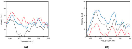
Figure 8.
Photoluminescence spectra of nanocrystals for three different deposition durations (black line—20 min, red line—40 min and blue line—60 min) after annealing: (a) at 800 °C, (b) at 1000 °C.
The peaks at 400, 408, 416, 434, 453, and 470 nm can be attributed to transitions associated with shallow defect states. The presence of the ~408 nm peak in all three samples indicates its stable nature. It most likely originates from a fundamental shallow donor, such as a selenium vacancy (VSe) [36]. The gradual simplification of this spectral region—from several sharp peaks in sample 1 to a more distinct set in samples 2 and 3—suggests the annealing of metastable shallow defects.
The emissions in the 490–590 nm range are clearly associated with deep defect states that act as radiative recombination centers.
Sample 1 exhibits several discrete peaks at 490, 529, 557, and 587 nm. These peaks are attributed to a broad distribution of deep defects, which may include various charge states of oxygen vacancies (VO0, VO+, VO2+) and different configurations of copper vacancies (VCu) [37].
The broad band at approximately 509–520 nm are caused by the recombination of donor-acceptor pairs (DAP) involving relatively deep defects, potentially pairs of copper vacancies and interstitial oxygen atoms (VCu-Oi) [38]. This process becomes thermodynamically favorable after intensive annealing.
The photoluminescence (PL) spectra of samples after annealing at 1000 °C are shown in Figure 8b. The peaks in the photoluminescence spectra in the range of 410–442 nm (3.02–2.81 eV) are attributed to electronic transitions involving shallow defects and near-band-edge processes [39]. The peaks in the 427–430 nm region are present in all three samples. They are likely the result of the recombination of free excitons or very shallow defect levels. This indicates the internal structure of a well-crystallized material [40]. The unique emission at 410 nm in sample 2 may indicate a specific crystalline phase or a particular configuration of surface states. It may be associated with interstitial selenium atoms (Sei) or quantum confinement effects in nanostructures [39]. The peaks at 469–478 nm are attributed to small copper vacancies (VCu), and the emission at 509–520 nm is probably due to the recombination of donor-acceptor pairs (DAP) involving copper vacancies (VCu) and interstitial oxygen atoms (Oi) [41,42]. Peaks at 555–562 nm are characteristic of copper vacancy complexes, while emission at 584–590 nm is attributed to selenium vacancy complexes (VSe) [43,44]. The thermal stability of defect-related emissions is of particular interest. The observed preservation of multiple discrete peaks after high-temperature treatment indicates the formation of energetically favorable defect complexes that exhibit stability under extreme thermal conditions. This phenomenon can be attributed to a combination of factors: the intrinsic stability of specific vacancy complexes within the cuprous selenide lattice, the potential influence of nanostructured morphology on defect stability through surface energy effects, and the dependence of defect formation energy on the stoichiometry [45].
The electrical properties of nanocrystals after high-temperature annealing depend largely on the phase composition of the material, as confirmed by measurements of current-voltage (CVC) characteristics.
Annealing at 800 °C improves the electrical characteristics of the material: the current–voltage characteristics curves become more linear and symmetrical (Figure 9a). This indicates an improvement in the crystal structure and contact quality. X-ray diffraction analysis shows that at this temperature, the phase composition of the material changes. The CuSe2O5 phase demonstrates a wide bandgap and a lower charge carrier concentration than CuSeO3 [46]. As a result, the current decreases to approximately 3 × 10⁻⁴ A.
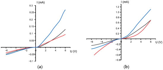
Figure 9.
Current–voltage characteristics of nanocrystals for three different deposition durations (black line—20 min, red line—40 min and blue line—60 min), after annealing: (a) at 800 °C; (b) at 1000 °C.
The transport mechanism in this phase can be described as thermally activated hopping. In this transport, charges (holes) are localized on Cu2+ ions and transfer between neighboring centers with the participation of phonons [47].
This type of conductivity is characteristic of copper-selenite oxide systems with strong charge localization and high interatomic barriers [48].
Heat treatment at 1000 °C resulted in a significant increase in current (up to ~1.2 mA) (Figure 9b). X-ray diffraction analysis showed that the material transitions to the triclinic CuSeO3 phase. This phase is characterized by a denser crystal structure and partial reduction of selenium centers, which in turn leads to a narrowing of the band gap (Eg ≈ 1.8–2.0 eV) and an increase in the number of free charge carriers [49].
4. Conclusions
As a result of the study, CuSeO3-NC/SiO2/SiO2/Si copper selenite nanocrystals were obtained for the first time by chemical deposition on a SiO2/Si track template. During thermal annealing, copper selenite demonstrated sequential phase transformations.
X-ray structural analysis confirmed that the synthesized samples represent the orthorhombic phase CuSeO3. Thermal annealing at 800 °C led to its transformation into the monoclinic phase CuSe2O5, and subsequent treatment at 1000 °C led to the formation of the triclinic polymorph CuSeO3. This sequence of transformations (orthorhombic → monoclinic → triclinic) indicates the transition of the system from a kinetically controlled state to a thermodynamically stable state at high temperatures.
Photoluminescence studies revealed a significant dependence of optical properties on phase composition. Shifts in the position and intensity of luminescence bands after annealing correlate with changes in the crystal lattice, band gap width, and concentration of defects acting as recombination centers. By controlling the presence of defects in copper selenite materials rather than eliminating them completely, optoelectronic functions can be adapted. This enables the creation of advanced solutions for sensor technology, lighting and energy conversion.
Measurements of current–voltage characteristics showed that phase transitions have a significant effect on the electrical conductivity of the material. The most significant change in conductivity is observed during the transition to the triclinic phase after annealing at 1000 °C, which is explained by the rearrangement of the crystal structure and a change in the charge transfer mechanism.
Thus, it has been established that thermal annealing is an effective tool for controlling the structure, optical and electrical properties of copper selenite. The demonstrated possibility of controlled phase transformation opens up prospects for the application of these materials in optoelectronics and sensor technology, where the fine-tuning of functional characteristics is required.
Author Contributions
Conceptualization, Z.B. and G.S.; methodology, A.A. (Aiman Akylbekova); software, A.A. (Ainash Abdrakhmetova); validation, A.D., A.A. (Abdirash Akilbekov) and D.J.; formal analysis, A.D. and A.A. (Abdirash Akilbekov); investigation, G.S.; resources, D.J. and L.K.; data curation, G.S.; writing—original draft preparation, G.S. and Z.B.; writing—review and editing, G.S. and Z.B.; visualization, A.U.; supervision, G.A.; project administration, G.S. All authors have read and agreed to the published version of the manuscript.
Funding
This research was funded by the Ministry of Science and Higher Education of the Republic of Kazakhstan (Grant No. AP25794781).
Data Availability Statement
The original contributions presented in this study are included in the article. Further inquiries can be directed to the corresponding authors.
Acknowledgments
This article was prepared as part of the implementation of the scientific project of grant funding for young scientists under the “Zhas Galym” project for 2025–2027 of the Science Committee of the Ministry of Science and Higher Education of the Republic of Kazakhstan AP25794781 «Synthesis and experimental and theoretical study of copper selenide-based nanogeterostructures in SiO2/Si track templates». During the preparation of this manuscript, the authors used GPT for the purposes of editing the author’s generated text, checking and improving English writing, and formatting references according to APA style. All unique ideas were developed, the literature and references were used in this paper, without the aid of AI.
Conflicts of Interest
The authors declare no conflicts of interest.
References
- Gul, B.; Alharbi, S.A.R.; Khan, M.S.; Aziz, S.M. Chalcogen-Mediated Band Tuning, Optoelectronic and Transport Properties of LaCuXO (X = Se, Te) Oxychalcogenides: First-Principles Study. Chem. Phys. Lett. 2025, 878, 142248. [Google Scholar] [CrossRef]
- Choudhury, P.; Behera, P.K.; Bisoyi, T.; Sahu, S.K.; Sahu, R.R.; Prusty, S.R.; Stitgen, A.; Scanlon, J.D.; Kar, M.; Rout, L. The Dehydrogenative Oxidation of Aryl Methanols Using an Oxygen Bridged [Cu–O–Se] Bimetallic Catalyst. New J. Chem. 2021, 45, 5775–5779. [Google Scholar] [CrossRef]
- Talib, H.; Bakr, N.A.; Abed, M.A. Synthesis and Characterization of Quaternary Chalcogenide Nanomaterials: A Review Study. Acad. Sci. J. 2024, 2, 322–360. [Google Scholar] [CrossRef]
- Aldakov, D.; Lefrançois, A.; Reiss, P. Ternary and Quaternary Metal Chalcogenide Nanocrystals: Synthesis, Properties and Applications. J. Mater. Chem. C 2013, 1, 3756–3776. [Google Scholar] [CrossRef]
- Arulraj, A.; Usmaniya, U.M.; Senguttuvan, G.; Sivakumar, V.; Khalid, M. Chalcogenides Nanocrystals and Its Applications. In Contemporary Nanomaterials in Material Engineering Applications; Springer: Cham, Switzerland, 2021; pp. 201–227. [Google Scholar]
- Hong, J.H.; Park, G.D.; Jung, D.S.; Kang, Y.C. Lithium Ion Storage Mechanism Exploration of Copper Selenite as Anode Materials for Lithium-Ion Batteries. J. Alloys Compd. 2020, 827, 154309. [Google Scholar] [CrossRef]
- Bonthula, S.; Pothu, R.; Srivastava, R.K.; Boddula, R.; Radwan, A.B.; Al-Qahtani, N. Recent Advances in Copper-Based Materials for Sustainable Environmental Applications. Sustain. Chem. 2023, 4, 19. [Google Scholar] [CrossRef]
- Effenberger, H. Die Kristallstrukturen von Drei Modifikationen des Cu(SeO3). Z. Krist. Cryst. Mater. 1986, 175, 61–72. [Google Scholar] [CrossRef]
- Tomar, R.; Kakkar, S.; Goyal, S.; Devi, M.M.; Bera, C.; Chakraverty, S. Multiple Helimagnetic Phases in Triclinic CuSeO3. J. Magn. Magn. Mater. 2020, 497, 165945. [Google Scholar] [CrossRef]
- Lee, S.; Lee, W.J.; Van Tol, J.; Kuhns, P.L.; Reyes, A.P.; Berger, H.; Choi, K.Y. Anomalous Spin Dynamics in the Coupled Spin Tetramer System CuSeO3. Phys. Rev. B 2017, 95, 054405. [Google Scholar] [CrossRef]
- Živković, I.; Djokić, D.M.; Herak, M.; Pajić, D.; Prša, K.; Pattison, P.; Dominko, D.; Micković, Z.; Cinčić, D.; Forró, L.; et al. Site-Selective Quantum Correlations Revealed by Magnetic Anisotropy in the Tetramer System SeCuO3. Phys. Rev. B Condens. Matter Mater. Phys. 2012, 86, 054405. [Google Scholar] [CrossRef]
- Dauletbekova, A.; Akylbekova, A.; Sarsekhan, G.; Usseinov, A.; Baimukhanov, Z.; Kozlovskiy, A.; Akilbekov, A.T. Ion-Track Template Synthesis and Characterization of ZnSeO3 Nanocrystals. Crystals 2022, 12, 817. [Google Scholar] [CrossRef]
- Dauletbekova, A.; Junisbekova, D.; Baimukhanov, Z.; Kareiva, A.; Popov, A.I.; Platonenko, A.; Khamdamov, J. Synthesis and Study of Oxide Semiconductor Nanoheterostructures in SiO2/Si Track Template. Crystals 2024, 14, 1087. [Google Scholar] [CrossRef]
- Jones, M.R.; Osberg, K.D.; Macfarlane, R.J.; Langille, M.R.; Mirkin, C.A. Templated Techniques for the Synthesis and Assembly of Plasmonic Nanostructures. Chem. Rev. 2011, 111, 3736–3827. [Google Scholar] [CrossRef] [PubMed]
- Akylbekova, A.; Dauletbekova, A.; Baimukhanov, Z.; Vlasukova, L.A.; Usseinov, A.; Saduova, N.; Popov, A.I. Annealing Effect on Structural, Optical and Electrophysical Properties of ZnSe Nanocrystals Synthesized into SiO2/Si Ion Track Template. Materials 2024, 17, 4149. [Google Scholar] [CrossRef] [PubMed]
- Akylbekova, A.; Mantiyeva, K.; Dauletbekova, A.; Akilbekov, A.; Baimukhanov, Z.; Vlasukova, L.; Abdihalikova, F. The Synthesis and Characterization of CdS Nanostructures Using a SiO2/Si Ion-Track Template. Crystals 2024, 14, 1091. [Google Scholar] [CrossRef]
- Coppola, N.; Ur Rehman, S.; Carapella, G.; Braglia, L.; Vaiano, V.; Montinaro, D.; Granata, V.; Chaluvadi, S.K.; Orgiani, P.; Torelli, P.; et al. Effects of In-Air Post Deposition Annealing Process on the Oxygen Vacancy Content in Sputtered GDC Thin Films Probed via Operando XAS and Raman Spectroscopy. ACS Appl. Electron. Mater. 2024, 6, 7135–7144. [Google Scholar] [CrossRef]
- Jagadish, K.A.; Kekuda, D. Thermal Annealing Effect on Phase Evolution, Physical Properties of DC Sputtered Copper Oxide Thin Films and Transport Behavior of ITO/CuO/Al Schottky Diodes. Appl. Phys. A 2024, 130, 315. [Google Scholar] [CrossRef]
- Becke, A.D. Density-Functional Thermochemistry. III. The Role of Exact Exchange. J. Chem. Phys. 1993, 98, 5648–5652. [Google Scholar] [CrossRef]
- Zicovich-Wilson, C.M.; Dovesi, R. On the Use of Symmetry-Adapted Crystalline Orbitals in SCF-LCAO Periodic Calculations. I. The Construction of the Symmetrized Orbitals. Int. J. Quantum Chem. 1998, 67, 299–309. [Google Scholar] [CrossRef]
- Zicovich-Wilson, C.M.; Dovesi, R. On the Use of Symmetry-Adapted Crystalline Orbitals in SCF-LCAO Periodic Calculations. II. Implementation of the Self-Consistent-Field Scheme and Examples. Int. J. Quantum Chem. 1998, 67, 311–320. [Google Scholar] [CrossRef]
- Dovesi, R.; Erba, A.; Orlando, R.; Zicovich-Wilson, C.M.; Civalleri, B.; Maschio, L.; Rérat, M.; Casassa, S.; Baima, J.; Salustro, S.; et al. Quantum-Mechanical Condensed Matter Simulations with CRYSTAL. Wiley Interdiscip. Rev. Comput. Mol. Sci. 2018, 8, e1360. [Google Scholar] [CrossRef]
- Mulliken, R.S. Electronic Population Analysis on LCAO-MO Molecular Wave Functions. II. Overlap Populations, Bond Orders, and Covalent Bond Energies. J. Chem. Phys. 1955, 23, 1841–1846. [Google Scholar] [CrossRef]
- Monkhorst, H.J.; Pack, J.D. Special Points for Brillouin-Zone Integrations. Phys. Rev. B 1976, 13, 5188–5192. [Google Scholar] [CrossRef]
- Horti, N.C.; Patil, N.R.; Inamdar, S.R.; Sannaikar, M.S.; Kamatagi, M.D. Synthesis and Optical Properties of Copper Oxide Nanoparticles: Effect of Solvents. J. Nanophotonics 2020, 14, 046010. [Google Scholar] [CrossRef]
- Sequeda, I.N.; Meléndez, A.M. Understanding the Role of Copper Vacancies in Photoelectrochemical CO2 Reduction on Cuprous Oxide. J. Phys. Chem. Lett. 2022, 13, 3667–3673. [Google Scholar] [CrossRef]
- O’Keeffe, M.; Moore, W.J. Thermodynamics of the Formation and Migration of Defects in Cuprous Oxide. J. Chem. Phys. 1962, 36, 3009–3013. [Google Scholar] [CrossRef]
- Fotopoulos, V.; Grau-Crespo, R.; Shluger, A.L. Thermodynamic Analysis of the Interaction Between Metal Vacancies and Hydrogen in Bulk Cu. Phys. Chem. Chem. Phys. 2023, 25, 9168–9175. [Google Scholar] [CrossRef]
- Varlamova, E.G.; Goltyaev, M.V.; Simakin, A.V.; Gudkov, S.V.; Turovsky, E.A. Comparative Analysis of the Cytotoxic Effect of a Complex of Selenium Nanoparticles Doped with Sorafenib, “Naked” Selenium Nanoparticles, and Sorafenib on Human Hepatocyte Carcinoma HepG2 Cells. Int. J. Mol. Sci. 2022, 23, 6641. [Google Scholar] [CrossRef]
- Li, J.; Bai, J.; Sui, T.; Cao, X.; Xu, M.; Sun, X.; Ju, X. Study on the Defects of KDP Crystal with Different States by the Positron Spectroscopy Method. CrystEngComm 2023, 25, 3051–3059. [Google Scholar] [CrossRef]
- Yu, Y.; Wuttig, M. Metavalent Bonding Impacts Charge Carrier Transport across Grain Boundaries. Nano Res. Energy 2023, 2, e9120057. [Google Scholar] [CrossRef]
- Meunier, G.; Bertaud, M. Constantes cristallographiques de CuSe2O5, CuSeO3 et Cu2SeO4. J. Appl. Crystallogr. 1976, 9, 364–366. [Google Scholar] [CrossRef]
- Kahn, O.; Verdaguer, M.; Girerd, J.J.; Galy, J.; Maury, F. Orbital Interactions in a Strongly Antiferromagnetically Coupled Copper(II) Linear Chain: CuSe2O5. Solid State Commun. 1980, 34, 971–975. [Google Scholar] [CrossRef]
- Möller, M.; Winter, H. Multiple Helimagnetic Phases in Triclinic CuSeO3. Phys. Rev. B 2019, 100, 024416. [Google Scholar] [CrossRef]
- Naik, C.C.; Mardolkar, S.; Salker, A.V. Microcube Formation and Characterization of Cobalt and Nickel Selenite Dihydrate: Thermal, Spectral, and Dielectric Insights. Inorg. Chem. Commun. 2024, 168, 112886. [Google Scholar] [CrossRef]
- Zhou, N.; Li, H.; Li, X.; Dang, Z.; Sun, Z.; Deng, S.; Li, J.; Xie, Y.; Xu, H.; Xia, F.; et al. Precise Synthesis and Broadband Photoresponse of Two-Dimensional Intrinsic Vacancy Semiconductor. Small Struct. 2024, 5, 2400062. [Google Scholar] [CrossRef]
- Zhang, W.F.; Zhang, M.S.; Yin, Z.; Chen, Q. Photoluminescence in Anatase Titanium Dioxide Nanocrystals. Appl. Phys. B 2000, 70, 261–265. [Google Scholar] [CrossRef]
- Blasse, G.; Grabmaier, B.C. Luminescent Materials; Springer: Berlin/Heidelberg, Germany, 1994; pp. 1–9. [Google Scholar] [CrossRef]
- Chow, P.K.; Jacobs-Gedrim, R.B.; Gao, J.; Lu, T.-M.; Yu, B.; Terrones, H.; Koratkar, N. Defect-Induced Photoluminescence in Monolayer Semiconducting Transition Metal Dichalcogenides. ACS Nano 2015, 9, 1520–1527. [Google Scholar] [CrossRef]
- Täuber, D.; Camacho, R.; Scheblykin, I.G.; Dobrovolsky, A. Exploring the Electronic Band Structure of Organometal Halide Perovskite via Photoluminescence Anisotropy of Individual Nanocrystals. Nano Lett. 2016, 16, 5087–5094. [Google Scholar] [CrossRef]
- Prakash, A.; Mishra, V.; Mahesha, M.G. Development of Enduring Interstitial Defects in Mg-Doped CuO Thin Films. RSC Adv. 2024, 14, 10004–10016. [Google Scholar] [CrossRef]
- Landsberg, P.T. Recombination in Semiconductors; Cambridge University Press: Cambridge, UK, 2003. [Google Scholar]
- Houck, D.W.; Shin, H.; Korgel, B.A.; Assaf, E.I.; Greene, R.M.; Pernik, D.R. Pervasive Cation Vacancies and Antisite Defects in Copper Indium Diselenide (CuInSe2) Nanocrystals. J. Phys. Chem. C 2019, 123, 9544–9551. [Google Scholar] [CrossRef]
- Nguyen, G.D.; Li, A.-P.; Liang, L.; Zou, Q.; Gai, Z.; Oyedele, A.D.; Fu, M.; Xiao, K.; Sumpter, B.G.; Liu, Z. 3D Imaging and Manipulation of Subsurface Selenium Vacancies in PdSe2. Phys. Rev. Lett. 2018, 121, 086101. [Google Scholar] [CrossRef] [PubMed]
- Alivisatos, A.P. Semiconductor Clusters, Nanocrystals, and Quantum Dots. Science 1996, 271, 933–937. [Google Scholar] [CrossRef]
- Canossa, S.; Bellè, E.; Delferro, M.; Predieri, G.; Graiff, C. Structural Motifs in Heteroleptic Copper and Cadmium Selenites. Inorg. Chim. Acta 2018, 470, 206–212. [Google Scholar] [CrossRef]
- Banerjee, S.; Altman, E. Variable-Range Hopping through Marginally Localized Phonons. Phys. Rev. Lett. 2016, 116, 116601. [Google Scholar] [CrossRef]
- White, S.; Banerjee, P.; Jain, P. Liquid-Like Cationic Sub-Lattice in Copper Selenide Clusters. Nat. Commun. 2017, 8, 14514. [Google Scholar] [CrossRef]
- Morozova, N.V.; Zhevstovskikh, I.V.; Korobeinikov, I.V.; Sarychev, M.N.; Semenova, O.I.; Sukhikh, T.S.; Ovsyannikov, S.V. A Monoclinic Crystal Structure and a Reusable Stress-Controlled Optoelectronic Switch in a Lead Halide Perovskite, CsPbBr3. J. Mater. Chem. C 2025, 13, 6453–6465. [Google Scholar] [CrossRef]
Disclaimer/Publisher’s Note: The statements, opinions and data contained in all publications are solely those of the individual author(s) and contributor(s) and not of MDPI and/or the editor(s). MDPI and/or the editor(s) disclaim responsibility for any injury to people or property resulting from any ideas, methods, instructions or products referred to in the content. |
© 2025 by the authors. Licensee MDPI, Basel, Switzerland. This article is an open access article distributed under the terms and conditions of the Creative Commons Attribution (CC BY) license (https://creativecommons.org/licenses/by/4.0/).