Abstract
This study investigated the effects of oxygen (O2) flow rates and annealing temperatures on optical, electrical, and structural properties of indium–gallium–zinc oxide (IGZO) film on glass substrates fabricated by using a co-sputtering system with two radio-frequency (RF) (In2O3 and Ga2O3) and one direct current (DC) (Zn) magnetron. The average transmittance and optical energy gap increased significantly when the oxygen flow rate was increased from 1 sccm to 3 sccm. An increased O2 flow during co-sputtering IGZO films caused the crystallinity of the InGaZn7O10 phase to increase, yielding a smoother and more uniform granular structure. The carrier mobility rose and the carrier concentration decreased with increasing O2 flow. The results of X-ray photoelectron spectra (XPS) analyses explained the impacts of the O2 flow rates and annealing temperatures on optical and electrical properties of the co-sputtered IGZO films. The optimum process conditions of the co-sputtered In2O3-Ga2O3-Zn films were revealed as an O2 flow rate of 3 sccm and an annealing temperature at 300 °C, which showed the largest average transmittance of 82.48%, a larger optical bandgap of 3.21 eV, and a larger carrier mobility of 7.01 cm2 V−1s−1. XPS results at various annealing temperatures indicated that the co-sputtered IGZO films with an O2 flow rate of 3 sccm have more stable chemical compositions among different annealing temperatures.
1. Introduction
In recent years, transparent amorphous oxide semiconductors (TAOSs) have received significant attention owing to their technologically significant characteristics, including high electron mobility, exceptional transparency, and the capability for low-temperature processing. Several TAOSs have been identified as promising channel materials for thin-film transistors (TFTs) in display applications [1,2]. The materials suitable for serving as the active layer in TFTs include Al-In-Zn-Sn-O [3], Al-Zn-Sn-O (AZTO) [4], amorphous In-Ga-Zn-O (α-IGZO) [5,6,7,8,9,10], In-Sn-O (ITO) [11], In-Zn-O (IZO) [12,13,14], ZnO [15], and Zn-Sn-O [16]. Among these, amorphous InGaZnO4 (IGZO) has garnered significant attention in research and development since Hosono and colleagues first showcased its potential as an active layer for TFTs [5]. One crucial aspect of TFTs based on TAOSs is their multicomponent composition, which grants them a high degree of flexibility in tuning the properties for TFT applications. Iwasaki et al. [17] indicated a combinatorial approach has been applied to TFTs by co-sputtering with three targets of In2O3, Ga2O3, and ZnO. Koinuma et al. [18] studied magnetron co-sputtering with three targets of In2O3, Ga2O3, and ZnO and elucidated the effects of each element on the structural, electrical, and optical properties of IGZO films. Bak et al. [19] studied Al-Zn-O and In2O3 and demonstrated that utilizing co-sputtering methods offers attractive advantages, including a wide range of material selection, facile control of film stoichiometry, and high deposition rates. Jeon et al. [20] investigated the influence of the Zn ratio on the microstructure of IGZO films and how this affected the performance of their transistor devices. They produced IGZO films with varying Zn ratios by co-sputtering two targets of InGaO and ZnO at different ZnO powers. With an increase in the Zn ratio from 0 to 0.69, the microstructure underwent a transformation from amorphous IGZO to nanocrystalline IGZO, and finally to columnar ZnO. These dynamic transitions in the microstructure had a significant impact on the electrical properties. Choi et al. [21] recently proposed the co-sputtered IGZO and ITO thin films as an interlayer source and drain (S/D) electrodes between ITO S/D electrodes and the IGZO channel layer to eliminate Schottky-like behavior in the output characteristics due to the creation of a potential barrier between the IGZO and ITO thin films The suggested TFT demonstrates enhanced electrical characteristics (µsat = 35.4 cm2 V−1s−1) in comparison to conventional ITO electrode-based TFTs (µsat = 9.1 cm2 V−1s−1) This improvement is attributed to reduce contact and channel resistance, along with the creation of a surface reaction between the S/D and channel layers. This reaction generates extra oxygen vacancies within the IGZO channel region. Park et al. [22] assessed the effects of nitrogen partial pressure in sputter deposition on the electrical properties and device reliability of a-IGZO TFTs. Incorporating nitrogen into IGZO provides an easy means of controlling the carrier concentration, thus altering the device performance. Furthermore, the introduction of nitrogen during conventional IGZO deposition significantly enhances the device reliability of N-doped IGZO TFTs in comparison to un-doped IGZO TFTs, attributed to the reduction in defect concentration. Cai et al. [23] investigated the effects of top surface treatment on the electrical performance of IGZO TFTs. The study revealed that effective passivation through the use of an octadecyltrichlorosilane (OTS) self-assembled monolayer (SAM) substantially improved the electrical performance of IGZO TFTs. Hong et al. [24] recently investigated the metal cation composition range of the IGZO system through atomic layer deposition (ALD) to achieve high mobility and robust device stability. The IGZO films with various compositions by sequential plasma-enhanced ALD (PEALD) were synthesized to evaluate the microstructure, physical, and electrical properties. All these findings offer an experimental foundation for comprehending the individual roles of each metal element in the In-Ga-Zn-O system and for developing combinatorial approaches to efficiently search for materials having improved performance. This information provides a guideline for adjusting the metallic compositions to meet the desired specifications for TFTs [17,24].
A previous study [25] investigated the influence of Ga2O3 power on the electrical properties of co-sputtered In2O3-Ga2O3-Zn (IGZO) films and the resulting TFTs. As the deposition power of Ga2O3 increased, there was a decrease in carrier concentration and mobility leading to an increased resistivity in the co-sputtered films. Another previous study [26] investigated the impacts of varied ZnO deposition power on the optical and electrical properties as well as the structure of co-sputtered IGZO films. The optimal process conditions for co-sputtering IGZO films exhibiting the highest film mobility, smoothest surface roughness, and the lowest residual stress were shown to have a ZnO deposition power of 100 W and an annealing temperature of 300 °C. In a third previous work [27], the effects of oxygen flows and annealing temperature on the properties of co-sputtered In2O3-Ga2O3-Zn films were investigated. In one study, Chen et al. [28] reported that the electrical measurements indicated a rise in resistivity with higher O2/Ar gas flow ratio and the band gap of the as-deposited IGZO films increased from 3.45 eV to 3.75 eV. This increase in resistivity was attributed to the reduction of oxygen vacancies as the O2/Ar flow ratio increased from 0% to 20%.
Moreover, the electrical and optical properties of IGZO films are commonly influenced by various preparation conditions and process parameters, including the type of substrate, the deposition methods, the working pressure, the substrate temperature, the final film thickness, and the O2/Ar flow ratio. Among these factors, the O2/Ar flow ratio is particularly significant as it profoundly impacts the film’s structure, tunes the optical band gap, and influences the electrical properties of IGZO films [28]. However, few studies have investigated the effects of the oxygen flow rate and annealing temperature on the optical, electrical, and structural properties of IGZO films fabricated by magnetron co-sputtering using three targets of In2O3, Ga2O3, and Zn. The present work investigates the effects of various oxygen (O2) flow rates and different annealing temperatures on the microstructure, phase formation, and the chemical composition, as well as the optical and electrical properties of co-sputtered IGZO films. The impact on the chemical composition and chemical bonding are analyzed using X-ray photoelectron spectroscopy (XPS). Finally, the most suitable O2 flow rate and annealing temperature for fabricating co-sputtered IGZO films will be recommended.
2. Materials and Methods
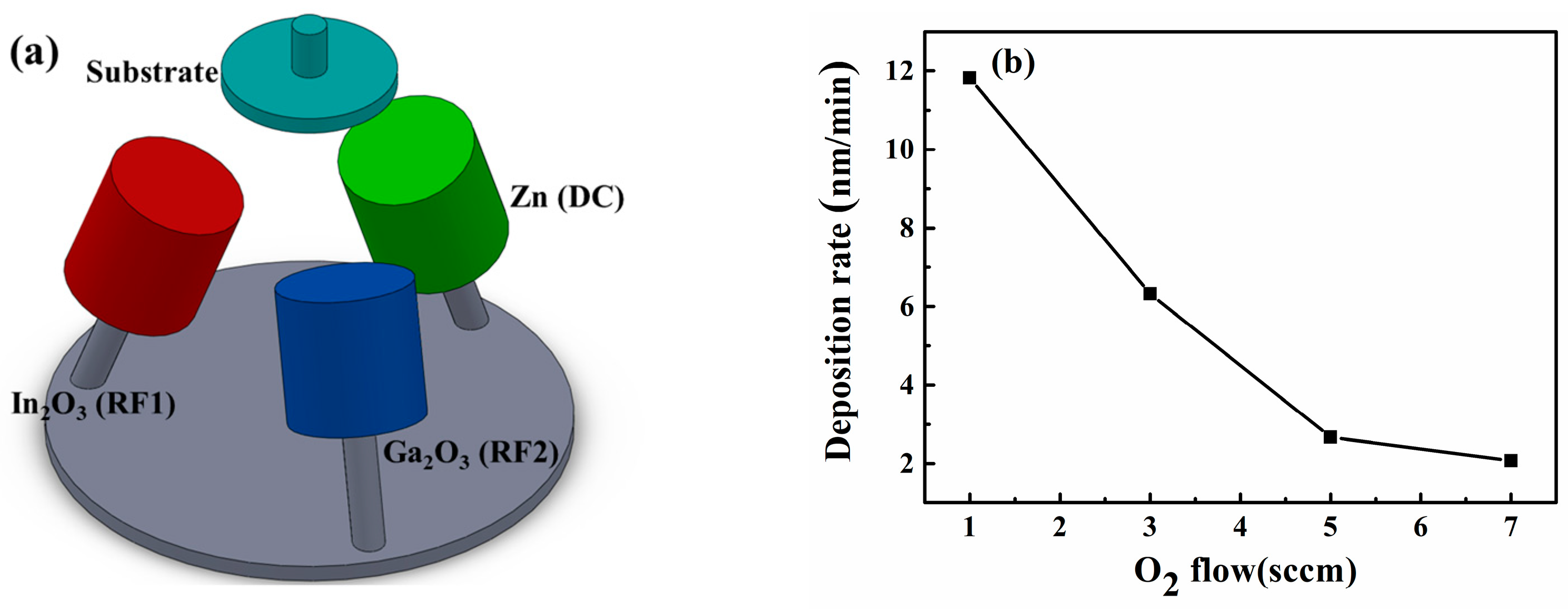
IGZO films were deposited on 1 × 1 cm2 square SCHOTT B270 glass substrates at room temperature using In2O3 (purity, 99.99%), and Ga2O3 (purity, 99.99%) ceramic targets and a Zn (purity, 99.99%) metallic target, all 7.62 cm (3″ in diameter, as shown in Figure 1a. Details of the preparation of targets are found elsewhere [29]. IGZO films were deposited using the following co-sputtering parameters, 40 W of direct-current (DC) power was used on a Zn target, and 75 W radio-frequency (RF) power was applied to both an In2O3 target and a Ga2O3 target, respectively. The deposition chamber was initially evacuated to 5.0 × 10⁻⁴ Pa, and then a fixed Ar gas flow of 30 sccm and an O2 gas flow varying from 1, 3, 5, or 7 sccm were introduced into the chamber to maintain a working pressure of 0.67 Pa. After deposition, the samples were annealed at 200, 300, or 400 °C at a working pressure of 0.67 Pa for 1 h in an ambient environment of 40 sccm N2. The thicknesses of the IGZO films deposited under different O2 flow rates were controlled within 200–215 nm. The film thicknesses were measured and fitted using a spectroscopic ellipsometer (SE) (M-2000U, J. A. Woollam Co., Inc., Lincoln County, NE, USA) and CompleteEASE software (version 5.30), respectively. The optical transmittance spectra of these films were examined in the wavelength range of 340–1200 nm using a UV–visible spectrophotometer (LAMBDA UV Lambda 900, PerkinElmer, Inc., Waltham, MA, USA). The film resistivity was performed with the four-point probe method using a 3S, MFP series (Swin). Hall measurements were performed with a HALL8800 system (Swin) using a magnetic field of 0.68 T and the van der Pauw method. The surface morphologies and roughness of the co-sputtered films were investigated using a scanning electron microscope (SEM) (JOEL JSM 6500-F, JEOL Ltd., Akishima, Tokyo, Japan) at an operating voltage of 15 kV and was observed using atomic force microscopy (AFM) (Veeco Dimension 3100, Plainview, NY, USA) at a scan area of 2 μm × 2 μm. The crystallinity of the co-sputtered IGZO films was also investigated using a grazing incidence X-ray diffraction (GIXRD) analysis (PANalytical X’Pert Pro, Malvern Panalytical Ltd., Malvern, UK) with a Ni-filtered Cu Kα (λ = 1.5418 Å) source at a glancing incident angle of 1°. The scanning range was between 2θ = 20° and 80°. X-ray photoelectron spectroscopy (XPS, Thermo VG Scientific Microlab 310F Instruments, Thermo Fisher Scientific Inc. Waltham, MA, USA) was also employed to characterize the chemical composition and chemical bonding states of the co-sputtered IGZO films. The binding energy calibration was performed using the C 1s peak at 284.5 eV. A data analysis of the O 1s peaks was employed using XPS Peak 4.0 software to enable the identification of chemical bond variations.
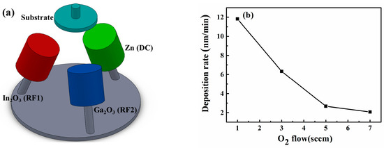
Figure 1.
(a) Schematic diagram of the co-sputtering system for the deposition of IGZO thin films; (b) Deposition rate of co-sputtered IGZO films as a function of O2 flow rate.
3. Results and Discussion
3.1. Optical and Electrical Properties of Cosputtered IGZO Films at Different Oxygen Flow Rates
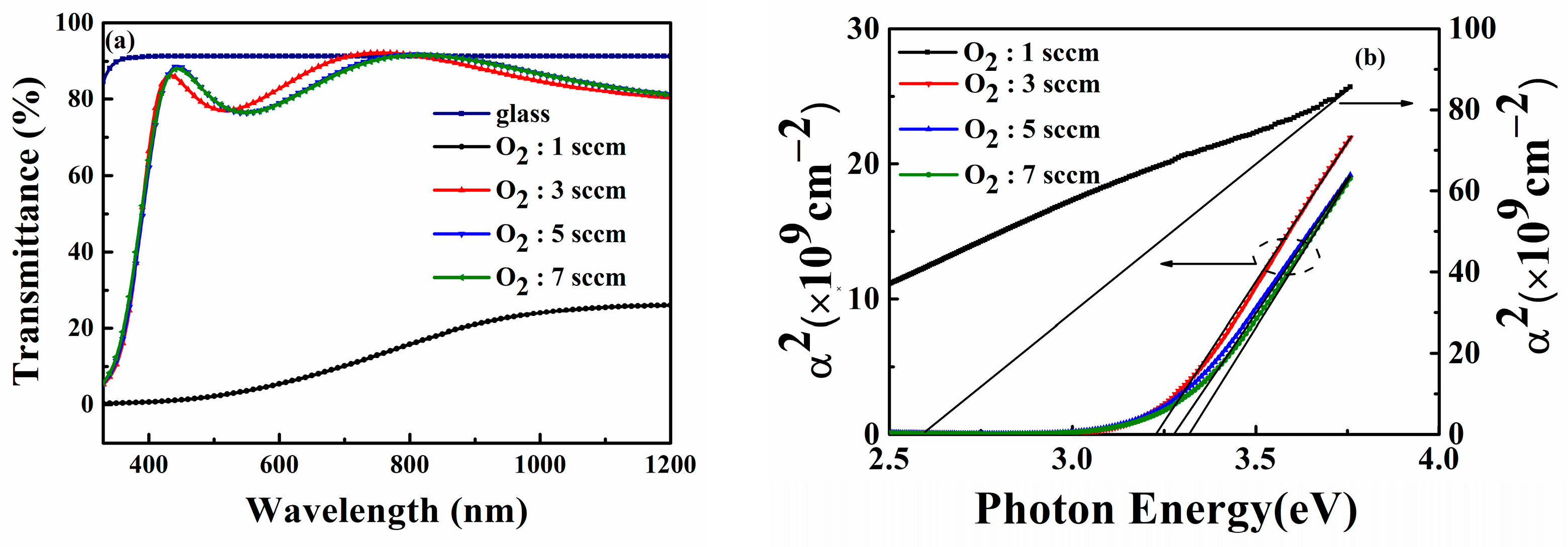
Figure 1b shows the deposition rate of co-sputtered IGZO films decreased rapidly from 11.81 to 2.07 nm/min when the O2 flow rate increases from 1 sccm to 7 sccm. This trend can be explained as follows: the increase in oxygen flow rate results in the scattering of sputtered atoms. Furthermore, oxygen might dilute argon gas, and collisions between sputtered target atoms and oxygen atoms on the substrate are intensified [28]. Compared with a single ceramic target (the composition of the target is In:Ga:Zn:O = 1:1:1:4), the deposition rate of IGZO films decreased rapidly from 3.974 to 1.427 nm/min by changing the flow rate of O2 from 0 to 6 sccm [28]. Utilizing the co-sputtering method provides higher deposition rates. Figure 2a shows the transmittance spectra of the co-sputtered IGZO films deposited with various O2 flow rates and annealed at 300 °C. The transmittance spectrum of the glass substrate B270 is also indicated. In terms of optical transmittance, IGZO films deposited at a low O2 flow rate of 1 sccm exhibit low transparency in the wavelength range of 340–1200 nm Additionally, there is a broad absorption tail, which could be attributed to oxygen deficiency or the presence of metallic interstitials [30,31]. The transmitted wavelengths of these films exhibited a shorter shift of wavelength in the photo-generative absorption threshold and a larger optical band gap (Eg) with an increased O2 flow rate. The transmittance in the ultraviolet region displayed a slight blue shift, resulting in an increase in the optical bandgap. The average transmittance (Tavg%) in the visible spectrum (400–800 nm) of the respective co-sputtered IGZO films deposited with O2 flow rates of 1, 3, 5, and 7 sccm annealed at 300 °C were 4.24%, 82.48%, 81.13%, and 81.03%, respectively. The Tavg% increased significantly from 4.24% to 82.48% as the O2 flow rate increased from 1 sccm to 3 sccm.
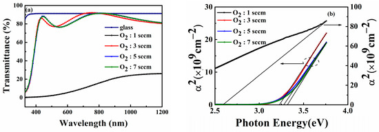
Figure 2.
(a) Transmittance spectra as a function of wavelength and (b) Plots of α2 versus the photon energy of co-sputtered IGZO films deposited with various O2 flow rates and annealed at 300 °C [27]. Reference [27] is the previous conference paper, of which the authors retain the copyright.
In a direct transition semiconductor, the absorption coefficient, α, and the optical band gap (Eg) are estimated using a standard Tauc plot method from the optical transmission spectra by [32,33],
where B is a constant, λ is the wavelength of the incident photon, hν is the energy of the incident photon, and T and d are the transmittance and thickness of the thin films, respectively. Figure 2b illustrates the plots of α2 versus the photon energy for co-sputtered IGZO films deposited at various O2 flow rates and annealed at 300 °C. Since the α of the IGZO thin films deposited at an O2 flow rate of 1 sccm is significantly greater than the α of the IGZO films deposited at other flow rates, α2 for the O2 flow rate of 1 sccm is displayed on the right vertical axis of Figure 2b. The optical bandgap (Eg) was determined by extrapolating the straight region of the plot of α2 versus the photon energy. The Eg of the respective co-sputtered IGZO films deposited with O2 flow rates of 1, 3, 5, and 7 sccm annealed at 300 °C were 2.53, 3.21, 3.26, and 3.30 eV, respectively. The Eg of the IGZO films annealed at 300 °C increased from 2.53 to 3.30 eV as the O2 flow rate increases from 1 to 7 sccm, which may be explained as the carrier concentration decreases for oxygen vacancies filled by oxygen atoms with increasing O2 introducing into the deposition process. The elevated oxygen partial pressure induces oxidation in a-IGZO and inhibits the presence of the oxygen vacancy defects that reside at the bottom of the conduction band [34,35]. Therefore, the inhibition of the formation of vacancy defects resulting from higher oxidation efficiency will conversely increase the Eg of thin films [36].
α2 = B(hν − Eg)
α = 2.303 × [log(1/T)]/d; hν = hc/λ
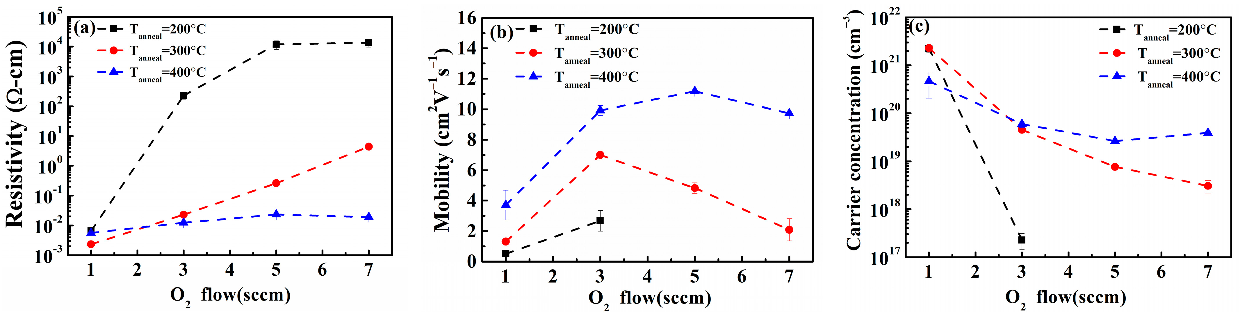
Figure 3a depicts the co-sputtered IGZO films’ resistivity as a function of O2 flow rate with different annealing temperatures, as measured by the four-point probe method. The results demonstrate that the resistivity increased as the oxygen flow rate increased for the films annealed at 200 °C and 300 °C. However, the resistivity remained relatively unchanged even with an increase in the O2 flow rate for the films annealed at 400 °C. Figure 3b shows the Hall mobility of the co-sputtered IGZO films as a function of O2 flow rate with different annealing temperatures. For the films annealed at 300 °C, the Hall mobility increased from 1.31 to 7.01 (cm2 V−1s−1) when the O2 flow rate increased from 1 to 3 sccm and then decreased with increasing O2 flow from 3 to 7 sccm. However, for the films annealed at 400 °C, as the O2 flow rate increased from 3 to 5 sccm the carrier mobility remained in the range of 9.92 to 11.18 (cm2 V−1s−1) The films deposited with an O2 flow rate of 5 sccm and an annealing temperature of 400 °C had the highest carrier mobility of all films tested, at 11.18 cm2 V−1s−1, after which it gradually decreases with increasing O2 flow. Figure 3c shows the carrier concentration of co-sputtered IGZO films as a function of O2 flow rate with different annealing temperatures. These results indicate that the carrier concentration decreased as the oxygen flow rate increased, although there was a slight increase in carrier concentration when the O2 flow rate was changed from 5 to 7 sccm for the films annealed at 400 °C. According to high resistance in co-sputtered IGZO films deposited with the O2 flow rates of 5 and 7 sccm and annealed at 200 °C, it is hard to measure the mobility and carrier concentration of the films using Hall measurement instruments.
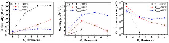
Figure 3.
(a) Four-point probe resistivity, (b) Hall mobility, and (c) carrier concentration of co-sputtered IGZO films as a function of O2 flow rate with different annealing temperatures [27]. Reference [27] is the previous conference paper, of which the authors retain the copyright.
3.2. Structural Analysis of Co-Sputtered IGZO Thin Films at Different Oxygen Flow Rates
To further validate the impact of the O2 flow rate on surface morphologies and roughness of the co-sputtered IGZO thin films, Figure 4 and Figure 5 present the SEM and AFM images, respectively, of co-sputtered IGZO thin films deposited at various O2 flow rates. Figure 4a–c show the SEM graphs of the co-sputtered IGZO films deposited under the respective O2 gas flow rates of 1, 3, and 5 sccm and annealed at 300 °C. Other annealing temperatures exhibited similar results. Figure 5a–c depict the AFM images of the co-sputtered IGZO films deposited under the respective O2 gas flow rates of 1, 3, and 5 sccm and annealed at 300 °C. The root-mean-square (RMS) roughness of the IGZO films deposited with O2 flow rates of 1, 3, and 5 sccm and annealed at 300 °C were 0.472, 0.411, and 0.513 nm, respectively, and these values are given in Figure 5. In summary, it can be observed that the surface morphology of the co-sputtered IGZO films appears rougher in structure when the O2 flow rate is 1 sccm. However, the surface morphology transitions to a smoother and more uniform granular structure when the O2 flow rate is increased to 3 sccm. At an O2 flow rate of 5 sccm, the grain size increases resulting in a rougher surface compared to that of 3 sccm. Thus, the AFM and SEM results reveal that the co-sputtered IGZO films deposited under an O2 flow rate of 3 sccm displayed the smoothest surface and the smallest RMS roughness. The surface conditions observed in these images explain why the Tavg% of co-sputtered IGZO films (shown in Figure 2a) increased significantly as the O2 flow rate increased from 1 sccm to 3 sccm.
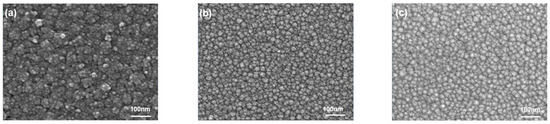
Figure 4.
SEM graphs (×15,000) for the IGZO films deposited with various O2 gas flows: (a) 1 sccm, (b) 3 sccm, and (c) 5 sccm and annealed at 300 °C.
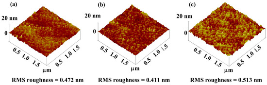
Figure 5.
AFM images and the RMS roughness of the IGZO films deposited with various O2 gas flows and annealed at 300 °C: (a) 1 sccm (200.08 nm), (b) 3 sccm (211.64 nm), and (c) 5 sccm (208.08 nm). The AFM scan area is 2 μm × 2 μm. The values in parentheses denote the thickness of each sample.
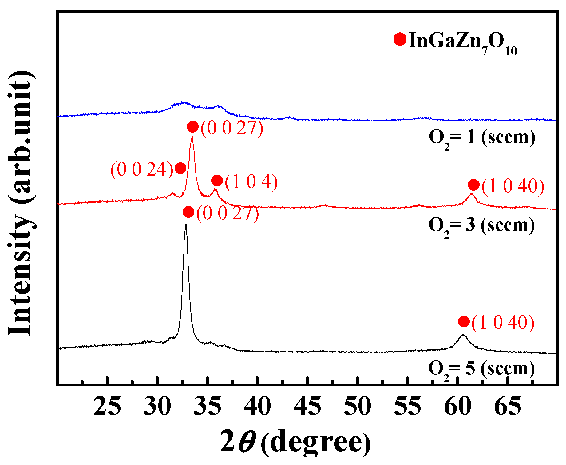
In order to verify the effects of different oxygen flow rates and annealing temperatures on the crystalline phases of co-sputtered IGZO films, the crystallinities of the IGZO films were also analyzed using glancing angle X-ray diffraction. Figure 6 shows the XRD graphs of co-sputtered IGZO films deposited under the respective O2 gas flow rates of 1, 3, and 5 sccm and annealed at 300 °C. Other annealing temperatures exhibited similar results. The IGZO films co-sputtered using three targets of In2O3, Ga2O3, and Zn with an O2 flow rate of 1 sccm exhibited an amorphous structure. However, the XRD patterns reveal a polycrystalline oxide film when the O2 flow rates were 3 sccm and 5 sccm, and the crystallinity increased as the O2 flow rate increased. The peak positions of InGaZn7O10 are, in order of intensity, (0 0 27), (1 0 40), (1 0 4), and (0 0 24), as informed by JCPDF #40-0257, with the strongest crystalline plane, (0 0 27) at 2θ ≈ 32.9° to 33.5°, appearing in the diffraction patterns when the O2 flow rate was in the range of 3 and 5 sccm. The average grain size (D) may be estimated by the full width at half-maximum (FWHM) of the InGaZn7O10 (0 0 27) diffraction peak using Scherrer’s equation [37]:
where λ is the wavelength of the X-ray (λ = 0.15406 nm), θ is Bragg’s diffraction angle, and β is the FWHM of the diffraction peak (in radians). Using this method, the co-sputtered IGZO films deposited at the respective O2 gas flow rates of 3 and 5 sccm yielded a grain size of about 9.9 nm and 11.5 nm, respectively. Therefore, the crystallinity and grain growth of the InGaZn7O10 phase were enhanced by increasing the O2 flow rate. A slight increase in the surface roughness was observed in the films with an O2 flow rate of 5 sccm (shown in Figure 4 and Figure 5) which is attributed to the creation and significant growth of crystalline IGZO grains in these films. Surface roughness plays a significant role in shaping the electron propagation within the IGZO films. The results of the structural analyses can explain why, with the O2 flow rate of 5 sccm, the carrier mobility slightly decreases to 4.82 cm2 V−1s−1 at an annealing temperature of 300 °C. Additionally, at an annealing temperature of 400 °C, the carrier mobility reaches the highest value of 11.18 cm2 V−1s−1, after which it gradually decreases.
D = 0.9λ/(β cosθ)

Figure 6.
XRD graphs of co-sputtered IGZO films deposited with O2 gas flow rates of 1, 3, and 5 sccm and annealed at 300 °C.
3.3. X-ray Photoelectron Spectroscop (XPS) ic Analysis of Co-Sputtered IGZO Thin Films
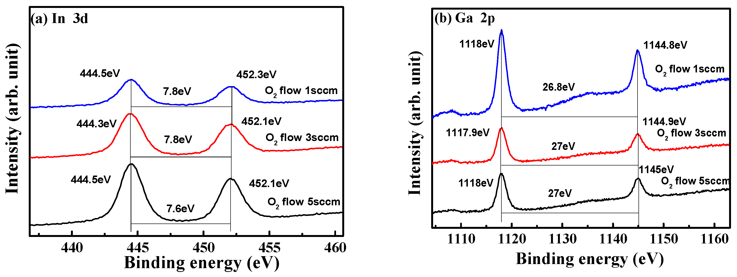
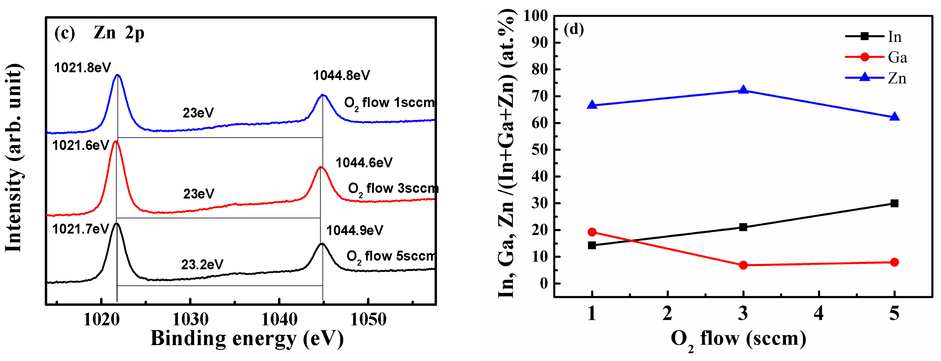
Figure 7 shows (a) In 3d, (b) Ga 2p, and (c) Zn 2p core levels of the XPS spectra for co-sputtered IGZO films deposited with O2 gas flow rates of 1, 3, and 5 sccm and annealed at 300 °C. The In 3d5/2 peak is centered at 444.5 eV, the Ga 2p3/2 peak is centered at 1118 eV, and the Zn 2p3/2 peak is centered at 1021.8 eV. According to previous research [38,39,40] the peak centers of In 3d5/2, Ga 2p3/2, and Zn 2p3/2 were reported to be 444.6 eV, 1118.9 eV, and 1021.8 eV, respectively, corresponding to In-O, Ga-O, and Zn-O bonds. However, if these peak positions shift to lower binding energies, it indicates that some of the bonding configurations In-In (443.8 eV), Ga-Ga (1117.4 eV), and Zn-Zn (1021.5 eV) are represented. Since the In 3d5/2 and Zn 2p3/2 core levels observed in the XPS spectra are consistent with those reported in previous studies [39,40], these findings suggest that indium and zinc are almost totally oxidized to In-O and Zn-O in the co-sputtered IGZO films. In addition, the Ga-O 2p3/2 peak is centered at 1118 eV, which is close to Ga-Ga (1117.4 eV) [40], indicating the presence of metallic Ga bonding in the co-sputtered IGZO films. Furthermore, the area of the Ga 2p3/2 peak gradually decreased with increasing O2 gas flow rate. Figure 7d shows the In, Ga, Zn/(In + Ga + Zn) atomic ratios (at.%) of co-sputtered IGZO films deposited with the O2 gas flow rates of 1, 3, and 5 sccm and annealed at 300 °C. The composition ratios were defined as the relative integrated intensity of In 3d5/2, Ga 2p3/2, and Zn 2p3/2 XPS peaks, respectively. It can be clearly observed that the Zn/(In + Ga + Zn) ratio increases from 66.51% to 72.15% when the O2 flow rate increases from 1 to 3 sccm, but after 5 sccm, the Zn/(In + Ga + Zn) ratio is reduced to a smaller ratio of 62.09%. The In/(In + Ga + Zn) ratio obviously increases from 14.24% to 29.93% when increasing the O2 flow rate from 1 to 5 sccm. The Ga/(In + Ga + Zn) ratio decreases from 19.25% to 6.83% when the O2 flow rate increases from 1 to 3 sccm, and at an O2 flow rate of 5 sccm, the Ga at.% slightly increases to 7.98%. Some articles mentioned that increasing the at% of Zn [8,20,25,26] and In [8,24] can enhance the carrier mobility of IGZO thin films. Therefore, it is expected that as the O2 flow rate increases, the carrier mobility will rise in tandem with the increase in Zn and In content. When the O2 flow rate is 5 sccm, due to the decrease in Zn at% (shown in Figure 7d) and the increase in AFM RMS roughness (shown in Figure 5c), the carrier mobility decreases to 4.82 cm2 V−1s−1, as indicated in Figure 3b. Because of the highest Zn at% and the lowest surface roughness is observed at an O2 flow rate of 3 sccm, the IGZO film exhibits the highest mobility of 7.01 cm2 V−1s−1 during the 300 °C annealing process. The surface morphology has crucial effects on the carrier mobility of the IGZO films [26].
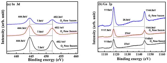
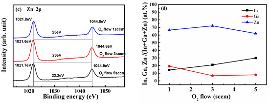
Figure 7.
XPS spectra of (a) In3d, (b) Ga2p, (c) Zn2p core levels, and (d) In, Ga, Zn/(In + Ga + Zn) atomic ratios (at.%) of co-sputtered IGZO films deposited with O2 gas flow rates of 1, 3, 5 sccm and annealed at 300 °C.
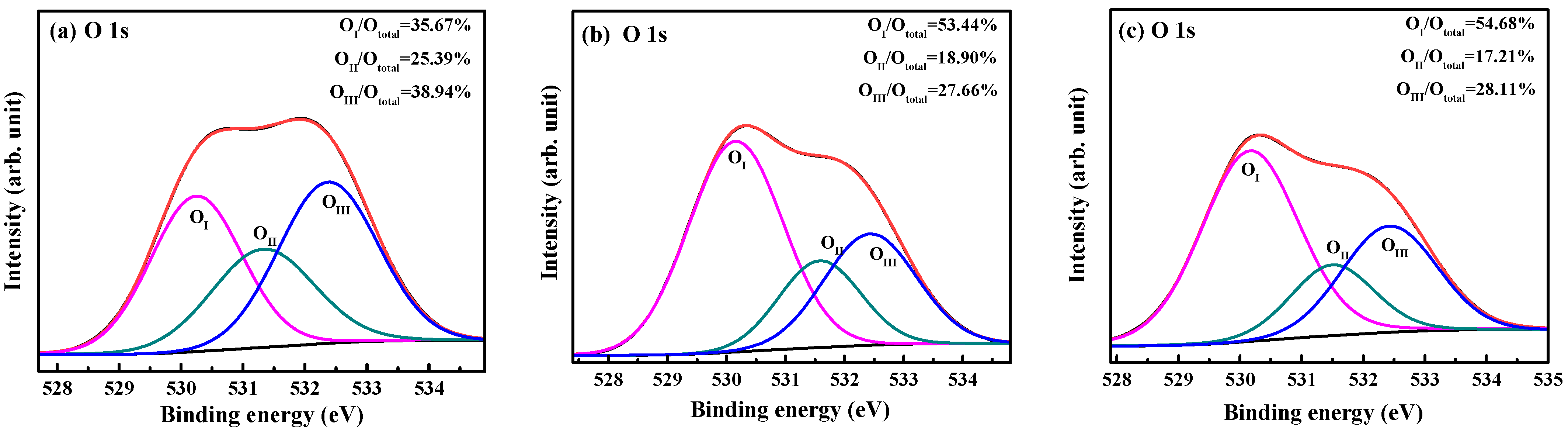
Figure 8a–c shows the O 1s peak spectra of co-sputtered IGZO films deposited with the respective O2 gas flow rates of 1, 3, and 5 sccm and annealed at 300 °C. The O 1s peak can be fitted by three nearly Gaussian distributions, centered at 530.3 ± 0.3, 531.3 ± 0.3, and 532.4 ± 0.3 eV, respectively [38,41]. To simplify the following descriptions, OI, OII, OIII, and Ototal refer to the areas of the components located at 530.3, 531.3, and 532.4 eV, and the total area of the O 1s peak, respectively. The black line represents the raw data, while the red line depicts the peak summation of the peaks OI, OII, and OIII. It is evident that the black lines are almost identical with the red lines. The component on the lower binding energy side of the O 1s spectrum at 530.3 eV (OI) can be attributed to O2− ions surrounded by Ga, In, and Zn atoms in the IGZO compound system [41]. The OI/Ototal values increased from 35.67% to 54.68% as the O2 flow rate increased. Therefore, the increase in O2− ions in the lattice leads to the increase in the average transmittance and optical bandgap, shown in Figure 2a,b, respectively. The binding energy component centered at 531.3 eV (OII) is associated with O2− ions that are in oxygen-deficient regions within the IGZO matrix [41]. The results show that the OII/Ototal values decreased from 25.39% to 17.21% with increasing O2 flow rate, indicating a decrease in the concentration of oxygen vacancies. Generally, oxygen vacancies are the main source of free electron carriers in IGZO films [35] and the decrease in OII-related oxygen vacancies results in the decrease in carrier concentration and the increase in resistivity. The high binding energy component located at 532.4 eV (OIII) is usually attributed to the presence of oxygen on the surface of film belonging to a specific loosely bound specie, e.g., –CO3 or adsorbed H2O or adsorbed O2 [41]. The OIII/Ototal values decreased from 38.94% to 27.66% with increasing O2 flow rate, indicating a decrease in the specific chemisorbed oxygen.
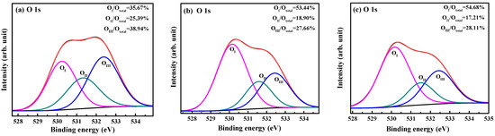
Figure 8.
O 1s peak spectra of co-sputtered IGZO films deposited with O2 gas flow rates of (a) 1, (b) 3, and (c) 5 sccm, and annealed at 300 °C.
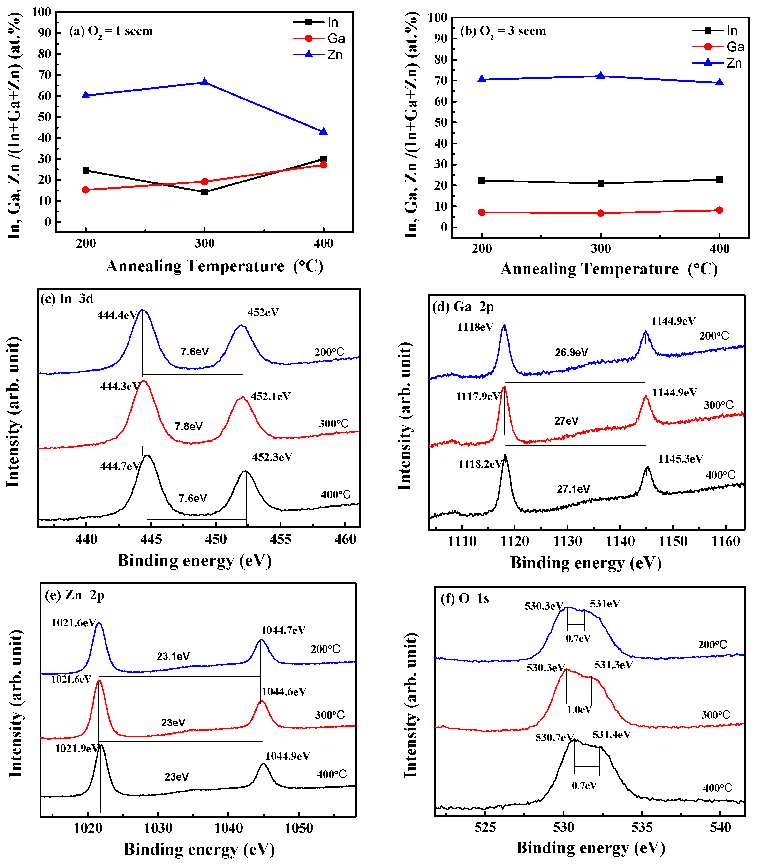
Figure 9a–b show the In, Ga, Zn/(In + Ga + Zn) at.% of co-sputtered films deposited at the respective O2 gas flow rates of 1 and 3 sccm among the different annealing temperatures. The XPS results revealed that the co-sputtered IGZO films with an O2 flow rate of 3 sccm have more stable chemical compositions among different annealing temperatures, whereas the co-sputtered IGZO films with an O2 flow rate of 1 sccm exhibit a more diverse chemical composition. Figure 9c–f show the XPS spectra of In 3d, Ga 2p, Zn 2p, and O 1s core levels for co-sputtered IGZO films deposited with an O2 gas flow rate of 3 sccm and subjected to different annealing temperatures. As the annealing temperature increased, the In 3d, Ga 2p, and Zn 2p binding energy shifted towards a higher energy by 0.3–0.4 eV, which is attributed to an increase in the oxidation state of In, Ga, and Zn. The results of the XPS spectra indicate that the In 3d and Zn 2s peaks were totally oxidized to In-O and Zn-O in the co-sputtered IGZO films, and the Ga-Ga bonds gradually transformed into Ga-O bonding configurations during annealing. Furthermore, the lower binding energy level of O 1s peaks shifted from 530.3 eV to 530.7 eV with an increase in the annealing temperature, and this was attributed to the increase in oxygen vacancies. In other words, the O atom is deficient on the surface of the IGZO film annealed at 400 °C in ambient N2.
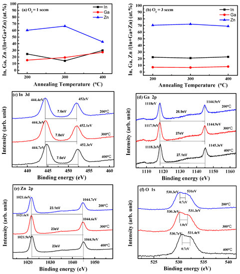
Figure 9.
In, Ga, Zn/(In + Ga + Zn) at.% of co-sputtered films deposited at the O2 gas flow rates of (a) 1 and (b) 3 sccm with different annealing temperatures; XPS spectra of (c) In3 d, (d) Ga 2p, (e) Zn 2p, and (f) O 1s core levels for co-sputtered IGZO films deposited with an O2 gas flow rate of 3 sccm and subjected to different annealing temperatures.
4. Conclusions
The average transmittance (Tavg%) and optical bandgap (Eg) of the co-sputtered IGZO films increased significantly when the oxygen flow rate was increased from 1 sccm to 3 sccm. The Eg of the IGZO films increased and the carrier concentration decreased with increasing O2 flow rates, which may be explained by oxygen vacancies being filled by oxygen atoms with increasing O2 during the deposition process. When the IGZO films were annealed at temperatures of 200 °C and 300 °C, the resistivity obviously increased with an increased O2 flow rate. With added O2 flow, the carrier concentration decreased and the Hall mobility rose, the latter reaching its highest value of 11.18 cm2 V−1s−1 when the O2 flow was 5 sccm. When the films were annealed at a temperature of 400 °C, the resistivity did not change with respect to an increased O2 flow rate.
The co-sputtered IGZO films with an O2 flow rate of 1 sccm exhibited an amorphous structure. The polycrystalline InGaZn7O10 phase and the crystallinity gradually increased when the O2 flow rate was increased from 3 sccm to 5 sccm. The surface morphology appears a rougher in structure when the O2 flow rate is 1 sccm. However, the surface morphology transitions to a smoother and more uniform granular structure with an increased O2 flow rate, which explains why the Tavg% of the co-sputtered IGZO films significantly increased as the O2 flow rate increased from 1 sccm to 3 sccm. The AFM results revealed that the co-sputtered IGZO film deposited with an O2 flow rate of 3 sccm displayed the smoothest surface and the smallest RMS roughness.
Due to the maximum Zn at% and the lowest surface roughness observed at the O2 flow rate of 3 sccm, the IGZO film demonstrates its highest mobility of 7.01 cm2 V−1s−1 during the 300 °C annealing process. The impacts of the O2 flow rate on Eg can be understood through the O 1s peak in the XPS spectra of the co-sputtered IGZO films annealed at 300 °C. A Gaussian fitting of the O 1s peaks revealed that increasing O2 gas flows led to an increase in OI bonding (O2− ions in the lattice), thereby yielding an increase in the Tavg% and the Eg, and a decrease in OII-related oxygen vacancies, thus resulting in a decreased carrier concentration and an increased resistivity. XPS results at various annealing temperatures indicated that the co-sputtered IGZO films with an O2 flow rate of 1 sccm exhibited a diverse chemical composition, whereas the co-sputtered IGZO films with an O2 flow rate of 3 sccm have more stable chemical compositions among different annealing temperatures.
A comprehensive assessment of the impacts of the O2 flows and annealing temperature on the optical, electrical and structural properties of co-sputtered In2O3-Ga2O3-Zn films suggests the following optimal process conditions. An O2 flow rate of 3 sccm and an annealing temperature at 300 °C showed the largest average transmittance of 82.48%, a larger optical bandgap of 3.21 eV, and a larger carrier mobility of 7.01 cm2 V−1s−1. This study is valuable for the applications of co-sputtered IGZO films in transparent thin-film transistors.
Author Contributions
The individual contributions of the authors are as follows. Conceptualization: Y.-S.L., S.-Y.Z. and Y.-Z.L.; methodology: S.-Y.Z. and Y.-Z.L.; software: S.-Y.Z., Y.-Z.L. and T.-C.T.; validation: S.-Y.Z. and Y.-Z.L.; formal analysis: S.-Y.Z. and Y.-Z.L.; investigation: S.-Y.Z. and Y.-Z.L.; resources: Y.-S.L.; data curation: S.-Y.Z. and Y.-Z.L.; writing—original draft preparation: Y.-S.L. and G.A.P.; writing—review and editing: G.A.P., Y.-S.L., S.-Y.Z., Y.-Z.L. and T.-C.T.; visualization: T.-C.T. All authors have read and agreed to the published version of the manuscript.
Funding
This research was funded by the Ministry of Science Technology Project (MOST 110-2637-E-159-004) and the National Science and Technology Council Project (NSTC 112-NU-E-159-001 –NU).
Data Availability Statement
All data that support the findings of this study are included within the article.
Acknowledgments
The authors extend appreciation to the Taiwan Semiconductor Research Institute (TSRI) for supplying the SEM, XPS, and XRD systems.
Conflicts of Interest
The authors declare no conflict of interest.
References
- Takagi, A.; Nomura, K.; Ohta, H.; Yanagi, H.; Kamiya, T.; Horano, M.; Hosono, H. Carrier transport and electronic structure in amorphous oxide semiconductor, a-InGaZnO4. Thin Solid Films 2005, 486, 38–41. [Google Scholar] [CrossRef]
- Hosono, H.; Kim, S.W.; Miyakawa, M.; Matsuishi, S.; Kamiya, T. Thin film and bulk fabrication of room-temperature-stable electride C12A7:e− utilizing reduced amorphous 12CaO·7Al2O3 (C12A7). J. Non-Cryst. Solids 2008, 354, 2772–2776. [Google Scholar] [CrossRef]
- Yang, S.; Cho, D.H.; Ryu, M.K.; Park, S.H.K.; Hwang, C.S.; Jang, J.; Jeong, J.K. High-Performance Al–Sn–Zn–In–O Thin-Film Transistors: Impact of Passivation Layer on Device Stability. IEEE Electron Device Lett. 2010, 31, 144–146. [Google Scholar] [CrossRef]
- Cho, D.H.; Yang, S.H.; Byun, C.W.; Shin, J.H.; Ryu, M.K.; Park, S.H.K.; Hwang, C.S.; Chung, S.M.; Cheong, W.S.; Yoon, S.M.; et al. Transparent Al–Zn–Sn–O thin film transistors prepared at low temperature. Appl. Phys. Lett. 2008, 93, 142111. [Google Scholar] [CrossRef]
- Nomura, K.; Ohta, H.; Takagi, A.; Kamiya, T.; Hirano, M.; Hosono, H. Room-temperature fabrication of transparent flexible thin-film transistors using amorphous oxide semiconductors. Nature 2004, 432, 488–492. [Google Scholar] [CrossRef] [PubMed]
- Hosono, H. Ionic amorphous oxide semiconductors: Material design, carrier transport, and device application. J. Non-Cryst. Solids 2006, 352, 851–858. [Google Scholar] [CrossRef]
- Yabuta, H.; Sano, M.; Abe, K.; Aiba, T.; Den, T.; Kumomi, H.; Nomura, K.; Kamiya, T.; Hosono, H. High-mobility thin-film transistor with amorphous InGaZnO4 channel fabricated by room temperature RF magnetron sputtering. Appl. Phys. Lett. 2006, 89, 112123. [Google Scholar] [CrossRef]
- Nomura, K.; Takagi, A.; Kamiya, T.; Ohta, H.; Hirano, M.; Hosono, H. Amorphous Oxide Semiconductors for High Performance Flexible Thin-Film Transistors. Jpn. J. Appl. Phys. 2006, 45, 4303–4308. [Google Scholar] [CrossRef]
- Jeong, J.K.; Yang, H.W.; Jeong, J.H.; Mo, Y.G.; Kim, H.D. Origin of threshold voltage instability in indium-gallium-zinc oxide thin film transistors. Appl. Phys. Lett. 2008, 93, 123508. [Google Scholar] [CrossRef]
- Park, J.S.; Jeong, J.K.; Chung, H.J.; Mo, Y.G.; Kim, H.D. Electronic transport properties of amorphous indium-gallium-zinc oxide semiconductor upon exposure to water. Appl. Phys. Lett. 2008, 92, 072104. [Google Scholar] [CrossRef]
- Miyasako, T.; Senoo, M.; Tokumitsu, E. Ferroelectric-gate thin-film transistors using indium-tin-oxide channel with large charge controllability. Appl. Phys. Lett. 2005, 86, 162902. [Google Scholar] [CrossRef]
- Dehuff, N.L.; Kettenring, E.S.; Hong, D.; Chiang, H.Q.; Wager, J.F.; Hoffman, R.L.; Park, C.H.; Keszler, D.A. Transparent thin-film transistors with zinc indium oxide channel layer. J. Appl. Phys. 2005, 97, 064505. [Google Scholar] [CrossRef]
- Yaglioglu, B.; Yeom, H.Y.; Beresford, R.; Paine, D.C. High-mobility amorphous In2O3–10wt%ZnO thin film transistors. Appl. Phys. Lett. 2006, 89, 062103. [Google Scholar] [CrossRef]
- Barquinha, P.; Goncalves, G.; Pereira, L.; Martins, R.; Fortunato, E. Effect of annealing temperature on the properties of IZO films and IZO based transparent TFTs. Thin Solid Films 2007, 515, 8450–8454. [Google Scholar] [CrossRef]
- Park, S.H.K.; Hwang, C.S.; Ryu, M.K.; Yang, S.H.; Byun, C.W.; Shin, J.H.; Lee, J.I.; Lee, K.M.; Oh, M.S.; Im, S.I. Transparent and Photo-Stable ZnO Thin-Film Transistors to Drive an Active Matrix Organic-Light-Emitting-Diode Display Panel. Adv. Mater. 2009, 21, 678–682. [Google Scholar]
- Hoffman, R.L. Effects of channel stoichiometry and processing temperature on the electrical characteristics of zinc tin oxide thin-film transistors. Solid-State Electron. 2006, 50, 784–787. [Google Scholar] [CrossRef]
- Iwasaki, T.; Itagaki, N.; Den, T.; Kumomi, H. Combinatorial approach to thin-film transistors using multicomponent semiconductor channels: An application to amorphous oxide semiconductors in In–Ga–Zn–O system. Appl. Phys. Lett. 2007, 90, 242114. [Google Scholar] [CrossRef]
- Koinuma, H.; Takeuchi, I. Combinatorial solid-state chemistry of inorganic materials. Nat. Mater. 2004, 3, 429–438. [Google Scholar] [CrossRef]
- Bak, J.Y.; Yang, S.; Yoon, S.M. Transparent Al–In–Zn–O Oxide semiconducting films with various in composition for thin-film transistor applications. Ceram. Int. 2013, 39, 2561–2566. [Google Scholar] [CrossRef]
- Jeon, H.; Na, S.; Moon, M.R.; Jung, D.; Kim, H.; Lee, H.J. The Effects of Zn Ratio on the Microstructure Electrical Properties of InGaZnO Films. J. Electrochem. Soc. 2011, 158, H949–H954. [Google Scholar] [CrossRef]
- Choi, S.-H. High-Performance Oxide TFTs with Co-Sputtered Indium Tin Oxide and Indium-Gallium-Zinc Oxide at Source and Drain Contacts. IEEE Electron Device Lett. 2021, 42, 168–171. [Google Scholar] [CrossRef]
- Park, K.; Kim, J.H.; Sung, T.; Park, H.-W.; Baeck, J.-H.; Bae, J.; Park, K.-S.; Yoon, S.; Kang, I.; Chung, K.-B.; et al. Highly Reliable Amorphous In-Ga-Zn-O Thin-Film Transistors through the Addition of Nitrogen Doping. IEEE Trans. Electron Devices 2019, 66, 457–462. [Google Scholar] [CrossRef]
- Cai, W.; Wilson, J.; Zhang, J.; Brownless, J.; Zhang, X.; Majewski, L.A.; Song, A. Significant Performance Enhancement of Very Thin InGaZnO Thin-Film Transistors by a Self-Assembled Monolayer Treatment. ACS Appl. Electron. Mater. 2020, 2, 301–308. [Google Scholar] [CrossRef]
- Hong, T.H.; Kim, Y.-S.; Choi, S.-H.; Lim, J.H.; Park, J.-S. Exploration of Chemical Composition of In-Ga-Zn-O System via PEALD Technique for Optimal Physical and Electrical Properties. Adv. Electron. Mater. 2023, 9, 2201208. [Google Scholar] [CrossRef]
- Lee, Y.S.; Chang, C.H.; Lin, Y.C.; Lyu, R.J.; Lin, H.C.; Huang, T.Y. Effects of Ga2O3 deposition power on electrical properties of cosputtered In–Ga–Zn–O semiconductor films and thin-film transistors. Jpn. J. Appl. Phys. 2014, 53, 05HA02. [Google Scholar] [CrossRef]
- Lee, Y.S.; Wang, C.W.; Lin, Y.C.; Jaing, C.C. Effects of ZnO composition on structure, optical and electrical properties of cosputtering In2O3–Ga2O3–ZnO films. J. Mat. Sci. Mat. Electron. 2016, 27, 11470–11477. [Google Scholar] [CrossRef]
- Lee, Y.-S.; Zhao, S.Y.; Lin, Y.Z.; Porter, G.A. Effects of oxygen flows and annealing temperature on properties of cosputtering In2O3-Ga2O3-Zn thin films. In Proceedings of the Compound Semiconductor Week (CSW), Toyama, Japan, 26–30 June 2016. [Google Scholar]
- Chen, X.F.; He, G.; Liu, M.; Zhang, J.W.; Deng, B.; Wang, P.H.; Zhang, M.; Lv, J.G.; Sun, Z.Q. Modulation of optical and electrical properties of sputtering-derived amorphous InGaZnO thin films by oxygen partial pressure. J. Alloys Compd. 2014, 615, 636–642. [Google Scholar] [CrossRef]
- Lee, Y.S.; Dai, Z.-M.; Lin, C.-I.; Lin, H.-C. Relationships between the crystalline phase of an IGZO target and electrical properties of a-IGZO channel film. Ceram. Int. 2012, 38, S595–S599. [Google Scholar] [CrossRef]
- Matsubara, K.; Fons, P.; Iwata, K.; Yamada, A.; Niki, S. Room-temperature deposition of Al-doped ZnO films by oxygen radical assisted pulsed laser deposition. Thin Solid Films 2002, 422, 176–179. [Google Scholar] [CrossRef]
- Beena, D.; Lethy, K.J.; Vinodkumar, R.; Mahadevan Pillai, V.P.; Ganesan, V.; Phase, D.M.; Sudheer, S.K. Effect of substrate temperature on structural, optical and electrical properties of pulsed laser ablated nanostructured indium oxide films. Appl. Surf. Sci. 2009, 255, 8334–8342. [Google Scholar] [CrossRef]
- Tang, Z.K.; Wong, G.K.L.; Yu, P.; Kawasaki, M.; Ohtomo, A.; Koinuma, H.; Segawa, Y. Room-temperature ultraviolet laser emission from self-assembled ZnO microcrystallite thin films. Appl. Phys. Lett. 1998, 72, 3270–3272. [Google Scholar] [CrossRef]
- Minegishi, K.; Koiwai, Y.; Kikuchi, Y. Growth of p-type Zinc Oxide Films by Chemical Vapor Deposition. Jpn. J. Appl. Phys. 1997, 36, L1453. [Google Scholar] [CrossRef]
- Bender, M.; Katsarakis, N.; Gagaoudakis, E.; Hourdakis, E.; Douloufakis, E.; Cimalla, V.; Kiriakidis, G. Dependence of the photoreduction and oxidation behavior of indium oxide films on substrate temperature and film thickness. J. Appl. Phys. 2001, 90, 5382–5387. [Google Scholar] [CrossRef]
- Carcia, P.F.; Maclean, R.F.; Reilly, M.H.; Nunes, G. Transparent ZnO thin-film transistor fabricated by rf magnetron sputtering. Appl. Phys. Lett. 2003, 82, 1117–1119. [Google Scholar] [CrossRef]
- Liu, W.T.; Liu, Z.T.; Yan, F.; Tan, T.T.; Tian, H. Influence of O2/Ar flow ratio on the structure and optical properties of sputtered hafnium dioxide thin films. Surf. Coat. Technol. 2010, 205, 2120–2125. [Google Scholar] [CrossRef]
- Song, D.; Windenborg, P.; Chin, W.; Aberle, A. Investigation of lateral parameter variations of Al-doped zinc oxide films prepared on glass substrates by RF magnetron sputtering. Sol. Energy Mater. Sol. Cells 2002, 73, 1–20. [Google Scholar] [CrossRef]
- Chen, J.; Wang, L.; Su, X.; Kong, L.; Liu, G.; Zhang, X. InGaZnO semiconductor thin film fabricated using pulsed laser deposition. Opt. Exp. 2010, 18, 1398–1404. [Google Scholar] [CrossRef]
- Hado, G.M.; Guerra, D.N.; Leinen, D.; Ramos-Barrado, D.J.; Marotti, R.E.; Dalchiele, E.A. Indium doped zinc oxide thin films obtained by electrodeposition. Thin Solid Films 2005, 490, 124–131. [Google Scholar]
- Kim, G.H.; Kim, H.S.; Shin, H.S.; Ahn, B.D.; Kim, K.H.; Kim, H.J. Inkjet-printed InGaZnO thin film transistor. Thin Solid Films 2009, 517, 4007–4010. [Google Scholar] [CrossRef]
- Chen, J.; Wang, L.; Su, X.; Wang, R. Pulsed laser deposited InGaZnO thin film on silica glass. J. Non-Cryst. Solids 2012, 358, 2466–2469. [Google Scholar] [CrossRef]


Disclaimer/Publisher’s Note: The statements, opinions and data contained in all publications are solely those of the individual author(s) and contributor(s) and not of MDPI and/or the editor(s). MDPI and/or the editor(s) disclaim responsibility for any injury to people or property resulting from any ideas, methods, instructions or products referred to in the content. |
© 2023 by the authors. Licensee MDPI, Basel, Switzerland. This article is an open access article distributed under the terms and conditions of the Creative Commons Attribution (CC BY) license (https://creativecommons.org/licenses/by/4.0/).