Article

Effect of UV and IR Radiation on the Electrical Characteristics of Ga2O3/ZnGeP2 Hetero-Structures

1
Laboratory for Radiophysical and Optical Methods of Environmental Studies, National Research Tomsk State University, 634050 Tomsk, Russia
2
Institute of High Current Electronics, Akademichesky Ave. 2/3, 634055 Tomsk, Russia
3
Institute of Physics of Microstructures RAS, Akademicheskaya St., 7, 603087 Nizhny Novgorod, Russia
*
Author to whom correspondence should be addressed.
Crystals 2023, 13(8), 1203; https://doi.org/10.3390/cryst13081203
Submission received: 30 May 2023 / Revised: 18 July 2023 / Accepted: 19 July 2023 / Published: 2 August 2023
(This article belongs to the Special Issue 1D and 2D Nanomaterials for Sensor Applications)

Abstract

:
The data on electrical and photoelectric characteristics of Ga2O3/ZnGeP2 hetero-structures formed by RF magnetron sputtering Ga2O3 target with a purity of (99.99%) were obtained. The samples are sensitive to UV radiation with a wavelength of λ = 254 nm and are able to work offline as detectors of short-wave radiation. Structures with Ga2O3 film that was not annealed at 400 °C show weak sensitivity to long-wavelength radiation, including white light and near-IR (λ = 808 and 1064 nm). After annealing in an air environment (400 °C, 30 min), ZnGeP2 crystals in contact with Ga2O3 show n-type conductivity semiconductor properties, the sensitivity of Ga2O3/ZnGeP2 hetero-structures increases in the UV and IR ranges; the photovoltaic effect is preserved. Under λ = 254 nm illumination, the open-circuit voltage is fixed at positive potentials on the electrode to Ga2O3, the short-circuit current increases by three orders of magnitude, and the responsivity increases by an order of magnitude. The structures detect the photovoltaic effect in the near-IR range and are able to work offline (remotely) as detectors of long-wavelength radiation.

1. Introduction

Technological progress is largely determined by obtaining high-quality semiconductor materials of complex composition. ZnGeP2 (ZGP) is a semiconductor compound with a chalcopyrite structure.
This is a p-type semiconductor with a bandgap Eg ≈ 2.0 eV at 300 K. ZGP crystals are characterized by a wide transparency region (0.65–12 µm), high second-order electrical susceptibility (d36 = 75 × 10−12 m/V), birefringence sufficient for phase matching, low-temperature dependence of refractive indices, relatively high thermal conductivity 0.18 W/(cm * K), resistance to high humidity and aggressive environments, large values of temperature, and angular and spectral phase-matching widths [1].
The electrical properties of ZnGeP2 have been studied less than other A2B4C52 compounds, which is explained by the experimental difficulties that arise when measuring transport effects in substances with high resistance. In [2], the results of studying a number of characteristics of ZGP crystals are presented. The Hall effect measurements showed that all samples had p-type conductivity. The concentration values for various crystals at T = 300° K and the types of impurities used are given in Table 1.
It can be seen from the results presented in [2] that the doping ZGP melt with group I chemical elements, practically, does not lead to a change in the hole concentration compared to the undoped crystal; however, the mobility of charge carriers decreases significantly. Group VI impurities cause an increase in the hole concentration by four orders of magnitude; they have the role of acceptors. The Hall mobility of holes decreased by approximately two orders of magnitude compared to undoped material, which probably indicated an increase in the concentration of impurity ions and structural lattice defects. A significant increase in the concentration of holes is observed when elements of group III, gallium, and indium are introduced into the melt. In these samples, a significant decrease in the value of the Hall mobility is observed, as in the case of sample 3p. Based on the results of the studies, it was determined that impurity elements of groups III and VI in the ZGP material are effective acceptor centers.
ZnGeP2 samples grown under various conditions and subjected to subsequent high-temperature annealing always have a p-type conductivity (from p0 = l × 1010 to 1 × 1016 cm−3) and a hole mobility of 20–40 cm2/V * s [3,4,5], which is explained by the presence of zinc vacancies [VZn] or germanium atoms at the sites of the phosphorus [GeP] sublattice. The invariability of the type of conductivity indicates high stability on the part of structural growth defects, which thus determines the properties of ZnGeP2.
Analyzing the temperature dependence of the electro-physical parameters in [2], the values of the activation energy of the acceptor impurity were estimated by 0.2–0.7 eV. The activation energies of deep centers increase with a decrease in the density of free holes in the studied crystals. A similar effect was also observed in [2] when doping ZnGeP2 with various impurities.
ZnGeP2 triple compounds are nonlinear crystals and are widely used in optical parametric oscillators, amplifiers, and other techniques based on the effects of nonlinear optics [6] like sources of coherent radiation of the mid-IR range, which are used in the following ways:
  • In LIDAR systems for remote detection and quantification of gases based on the effect of resonant absorption. The range from 3 to 10 μm is most effective [7];
  • In medicine, e.g., minimally invasive neurosurgery (tissue ablation) with a wavelength of 6.45 μm, requiring single high-energy pulses [8];
  • In the evaporation and deposition of thin-film polymers;
  • In spectroscopy and other scientific applications where high spatial and temporal resolution is required, e.g., excitation and vibrational transitions in molecules or inter-band transitions in semiconductor structures;
  • Special military and civilian applications.
In addition to the applications aforementioned, this work presents the results of studies of electrical and photoelectric characteristics of structures based on ZnGeP2 and gallium oxide films, and their sensitivity to ultraviolet and infrared radiation.
Ga2O3 is a transparent conducting oxide (TCO) that forms several polymorphs, such as α, β, γ, δ, and ε [9,10,11], which can either be insulators or conductors depending on the growth conditions from different techniques. Each polymorph can exhibit differences in band alignment [12]. Polymorphs have slightly varying material properties in the crystal space group. Differences between polymorphs include their properties in the crystal space group and the coordination number of Ga3+ ions. Ga2O3 is an n-type semiconductor with a bandgap of Eg = 4.8–5.3 eV. In the band gap of Ga2O3, there are local levels of defects, mainly due to oxygen and gallium vacancies [13].
Gallium oxide has a number of practical properties, where Ga2O3 is a semiconductor of n-type conductivity with a high specific resistance (ρ ≈ 1013 Ω·cm) that allows us to create fluorescent capacitors with a wide set of wavelengths and gas sensors with high stability and speed of operation even in conditions of high humidity. The use of oxide films in semiconductor/Ga2O3 structures allowed for the development of various devices for detecting UV radiation in outer space, flame detectors, and tracking the state of ozone holes.
The properties of the materials and the characteristics of the semiconductor/Ga2O3 interfaces depend on the method of manufacture, the thickness of the deposited layers [14], the pressure of the gas mixture during manufacture [15,16], and subsequent technological processes [17,18]. In turn, the processes at these interfaces determine the electrical and optical characteristics of the structures when thin layers of gallium oxide are used. Often devices of short-wave range, according to technical specifications, work in continuous modes of UV radiation, including systems of protected short-range communication, UV astronomy, and monitoring of ozone holes. In this regard, it is important to study the detector behavior under UV continuous illumination. One of the promising areas of development of short-wave radiation detectors is devices that can operate as self-powered UV photodetectors. Such photodetectors have a simple design and, most importantly, involve direct integration with metal–dielectric–semiconductor (MDS) fabrication technology.

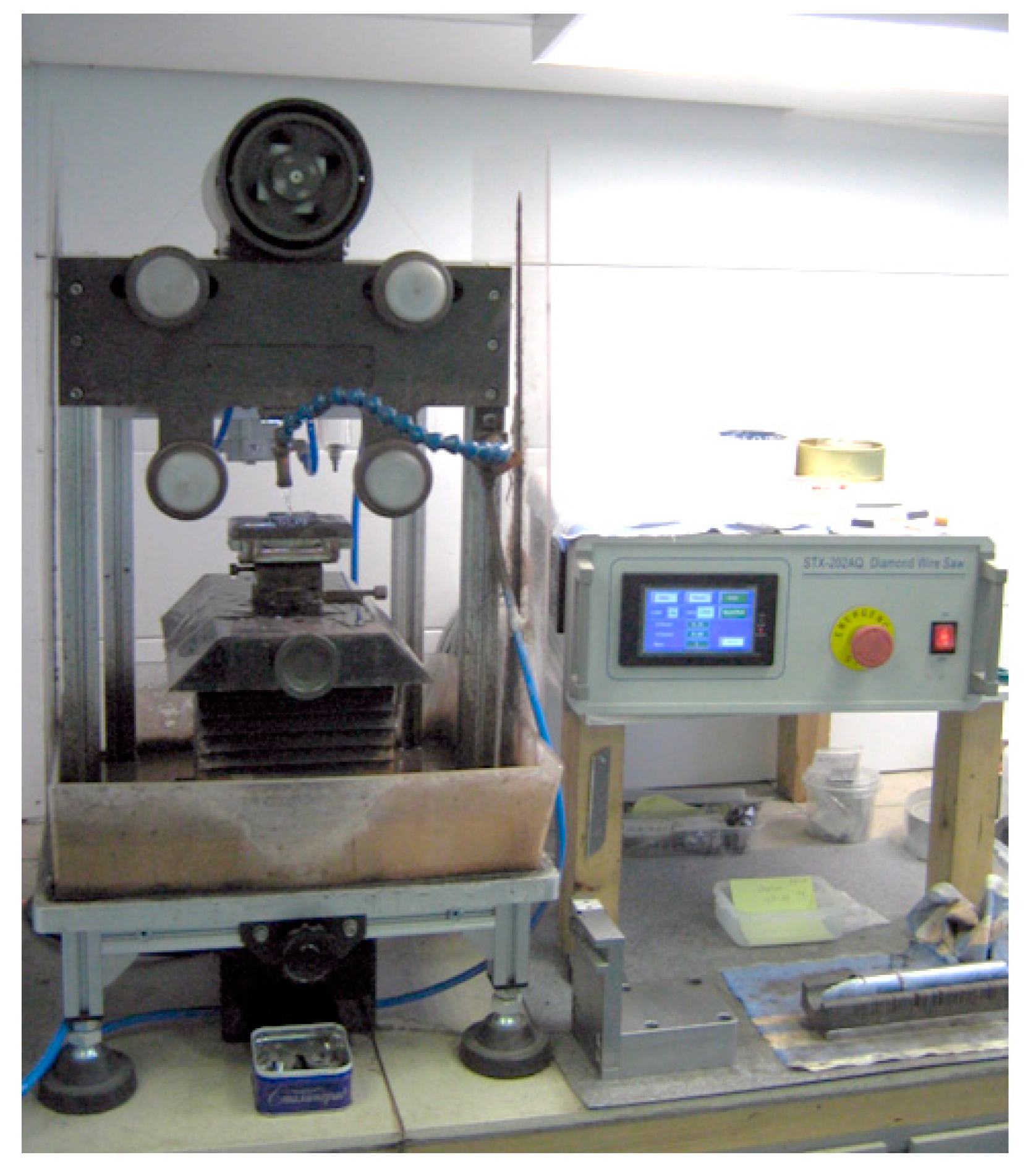
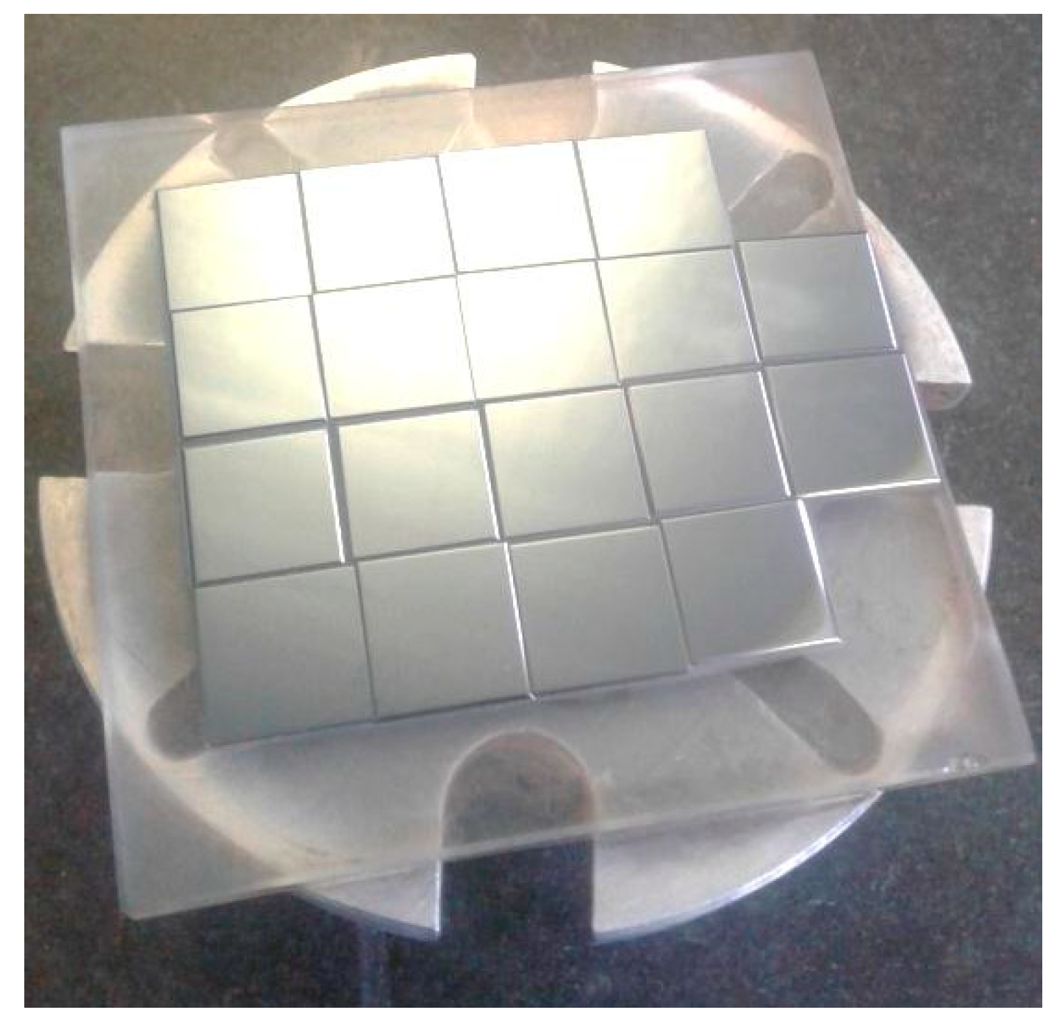
2. Preparation of ZGP Substrates

A wire-cutting machine was used to cut ZGP ingot into plates with dimensions of 6 × 6 × 1 mm. The wire used in Figure 1 is a wire with a diameter of 0.08–0.35 mm. A wire was used to improve cutting, on which a diamond-containing layer with a grain size of 10–60 µm was galvanized. The main advantage of wire cutting is that this method makes it possible to obtain formed parts with minimal disruption of the crystal structure due to low thermodynamic stresses that occur in the zone of contact between the wire and the workpiece. When processing brittle materials, the force is about 0.15–2.00 N.
The plates obtained after cutting had non-flatness and non-parallelism, a significant thickness of the damaged layer, and a spread in thickness. Technological operations of grinding and polishing were sequentially carried out to obtain the specified values of the thickness and surface roughness.
The block of elements was attached to the faceplate using wax glue and fixing equipment. Grinding was realized by the free-lapping principle. The abrasive suspension is collected from distilled water and diamond powder of the selected grain size, which is selected from the given specification of the roughness class.
During the grinding process, the abrasive grains, which are not connected, form an abrasive layer between the ZIP plates and the grinder, and rolling the particles of both the processed material and the material of the grinder break out. On the processed plates, the material is removed only from the side facing the grinder; the second side is the base.
When rotating in the same direction as the grinder and the faceplate with a block of elements, the grains of the abrasive grains are pressed with one of their faces into the grinder, and with the other, into the surface of the plates to be machined. In places of contact with abrasive grains, cracks appear on the surface of the grinder and elements, the maximum depth of which depends on the nature and size of the fractions of the selected abrasive grains. When, because of repeated impacts of grains, the entire surface layer is covered with similar cracks, subsequent grain movements in the same places will lead to the extraction of fragments of the plate and form “gouges”. A number of adjacent gouges form a characteristic rough surface.
Polishing of optical elements is the final operation and aims to eliminate surface damage after grinding and to ensure high cleanliness (Figure 2) of the treated surface.
The initial polishing of the working surfaces of all the studied samples was carried out on a 4-PD-200 polishing and finishing machine (SZOS, Republic of Belarus). The initial processing of the working surfaces of the samples consisted of polishing on a cambric-polishing pad using synthetic diamond powder ACM 0.5/0 (average grain size 270 nm). Next, the samples were additionally polished on a cambric polishing pad using synthetic diamond powder ACM 0.25/0. The samples were then polished on a resin polishing pad made from polishing resin using ACM 0.25/0 synthetic diamond powder.

3. Experimental Methodology

The Ga2O3/ZnGeP2 structures were formed by depositing a Ga2O3 film by RF magnetron sputtering Ga2O3 (99.99%) target onto polished ZnGeP2 substrates.
Thin layers of gallium oxide were obtained on an AUTO-500 unit (manufacturer: Edwards) in an Ar/O2 gas mixture. The oxygen concentration in the mixture was maintained at (56.1 ± 0.5) vol.%. The distance between the target and the substrate was 70 mm. The pressure in the chamber during deposition was 0.7 Pa. During the deposition of the oxide film, the ZGP substrates were not heated. After the formation of the Ga2O3 film with a thickness of 150–200 nm, Pt electrodes were deposited on the Ga2O3 film through a metal mask, where the contact area to Ga2O3 is of s = 1.04 × 10⁻² cm2. A solid ohmic contact (In) was deposited onto the opposite surface of the ZnGeP2 substrate. Schematic of the device structure is presented in Figure 3. Some of the samples were annealed in the air for 30 min at 400 °C.
The current–voltage characteristics (I-V), when no radiation (dark) and under UV illumination, were measured at room temperature using a Keithley 2611B source meter. A VL-6.C krypton-fluorine lamp with a 254 nm filter was used as a source of UV radiation (UVr). The distance between the lamp and the sample was 1 cm, the radiation power was 8 × 10⁻⁶ W, and the incident radiation intensity was 0.78 mW/cm2. When working in the IR range, lasers at 808 and 1064 nm were used. Regardless of the type of radiation, the samples were illuminated from the side of the oxide film.

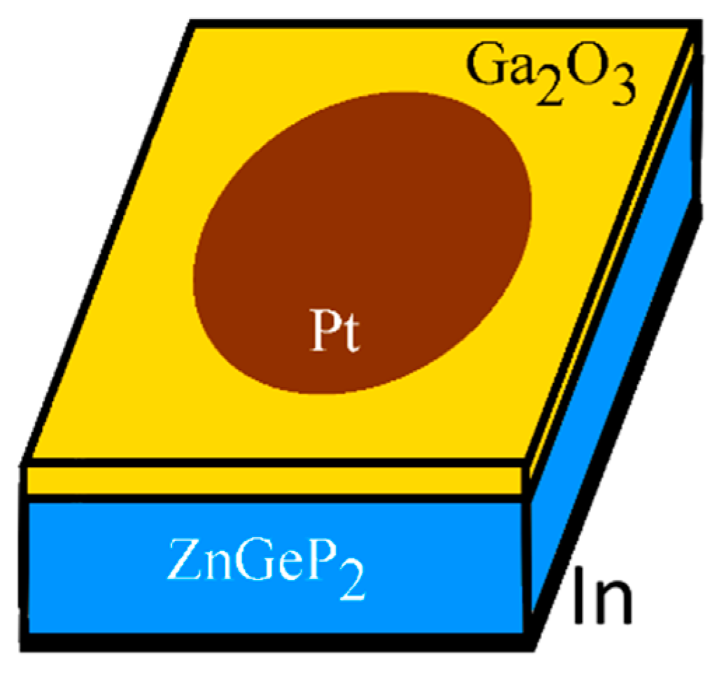
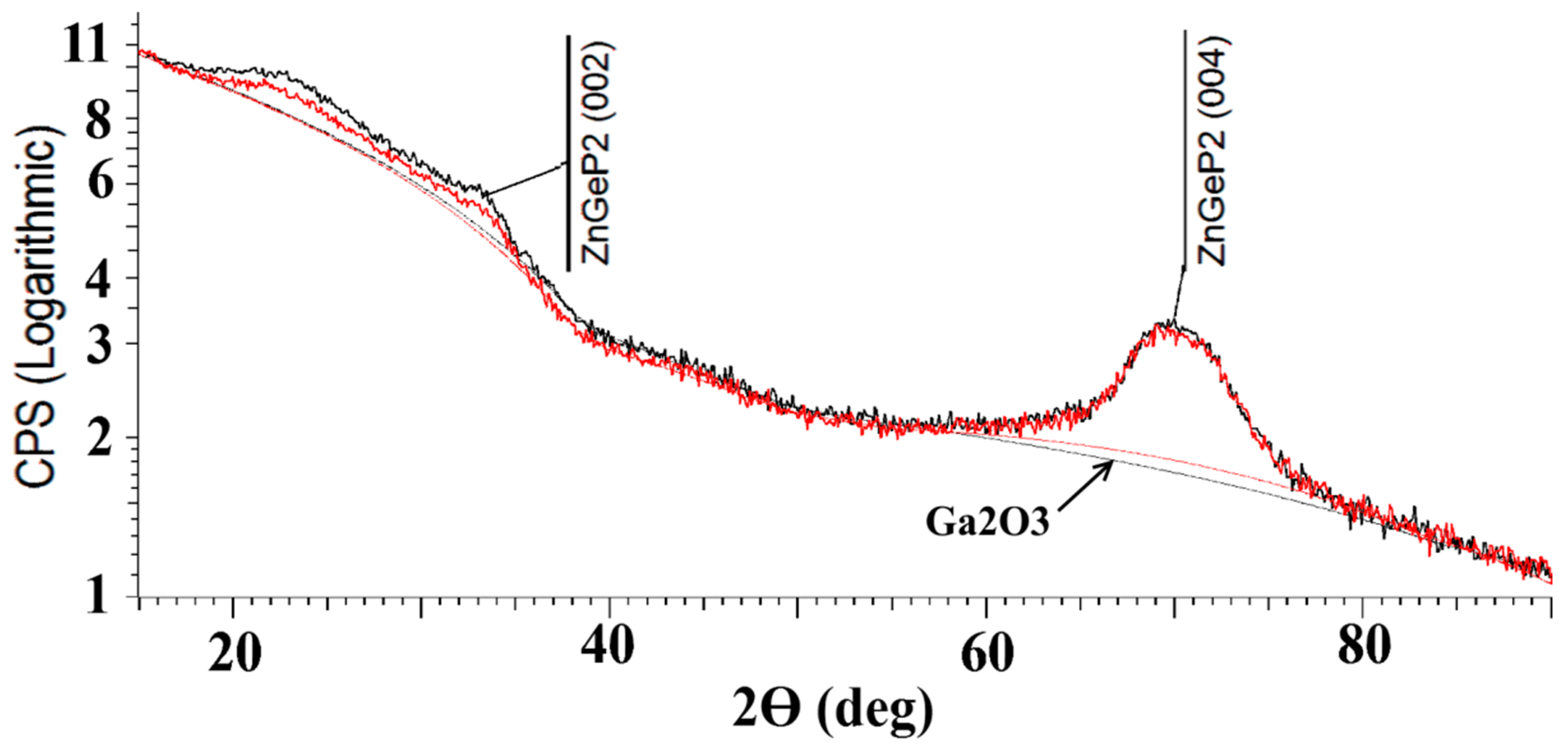
4. Experimental Data and the Discussion

Figure 4 shows the data of X-ray diffraction analysis of a gallium oxide film deposited on a ZnGeP2 substrate by RF magnetron sputtering Ga2O3 (99.99%) target. The absence of peaks in the curve for Ga2O3 indicates the amorphous phase of the oxide film.

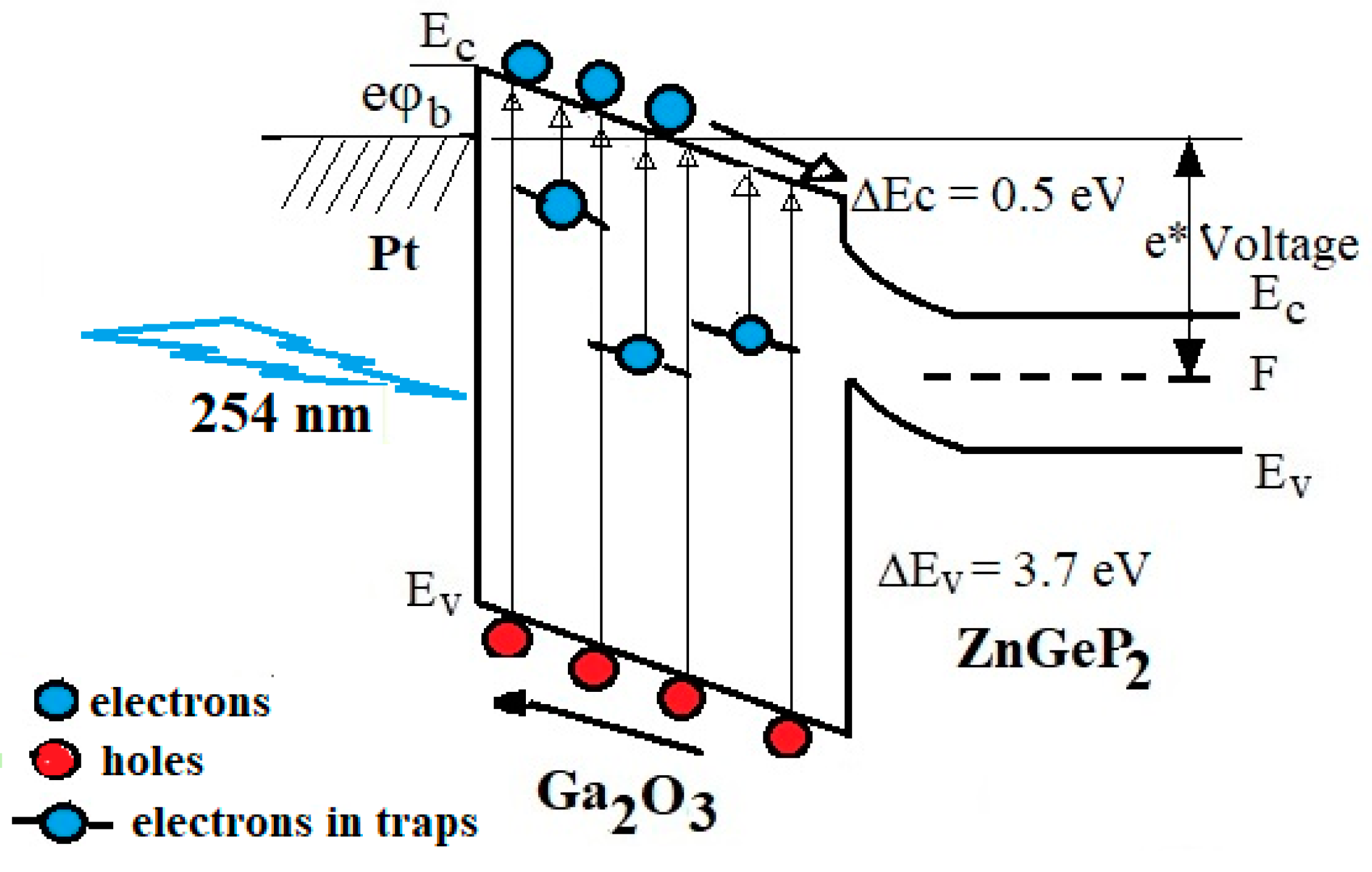
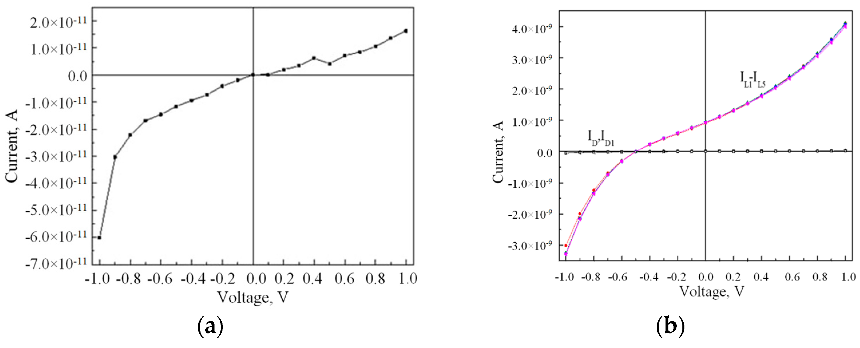
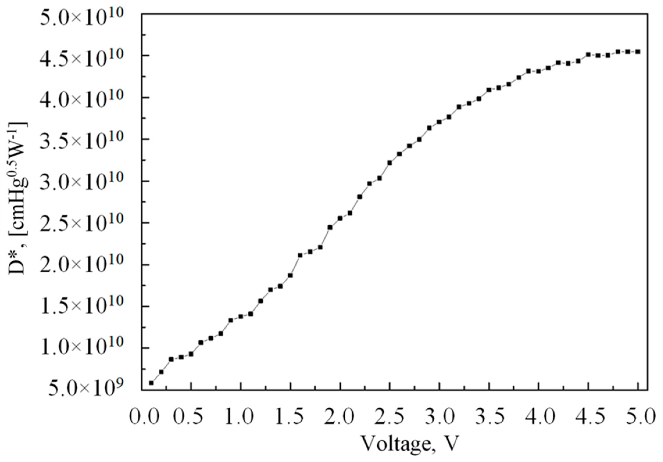
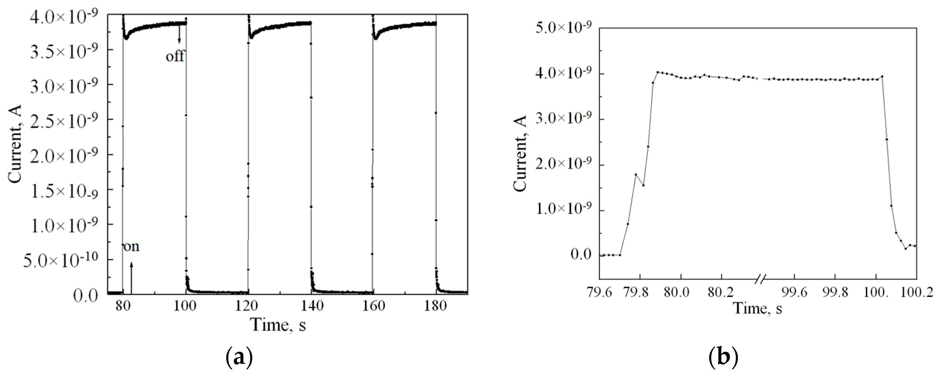
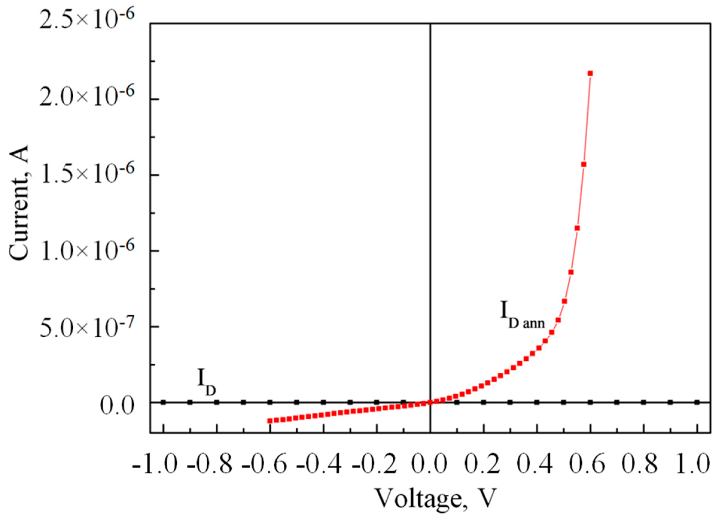
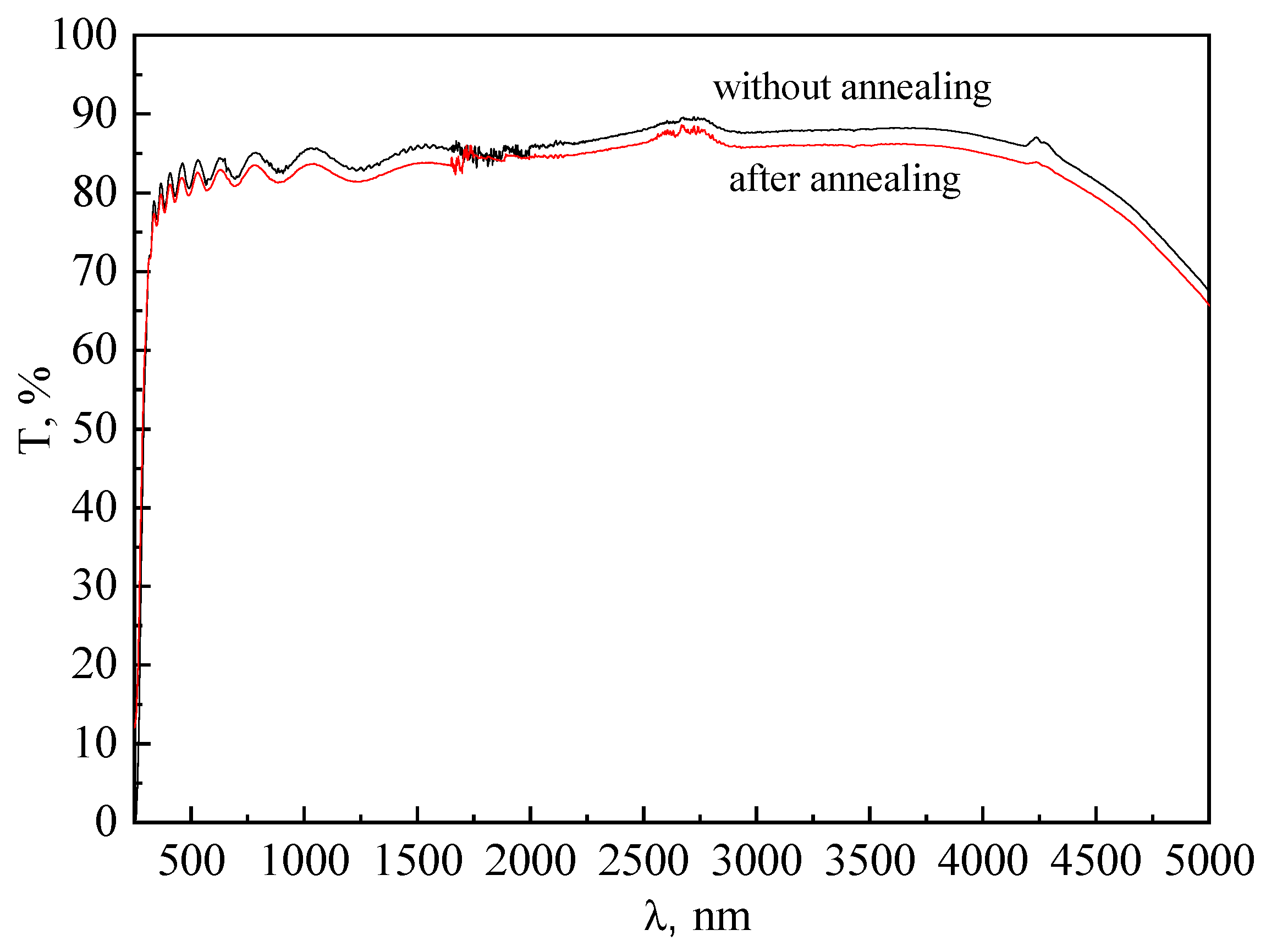
4.1. Electrical and Photoelectric Characteristics of Structures without Annealing

Figure 5 shows a schematic representation of the energy diagram of the Ga2O3/ZnGeP2 hetero-structure. Taking into account the electronic affinity of the materials in contact (χGa2O3 = 4.0 eV, χZGP = 3.5 eV), the band offset of the conduction band is ΔEc = 0.5 eV, and the valence band is ΔEv = 3.7 eV (Eg1 = 5.1 eV and Eg2 =1.9 eV).
The current–voltage (I-V) characteristics of Ga2O3/ZnGeP2 structures without annealing at 400 °C are not symmetrical with respect potential sign on the Pt electrode: at negative potentials on the contact to gallium oxide, the current increases faster than at positive values of V, which corresponds to direct currents (Figure 6a).
Under UV illumination, electrons from the valence band and from deep centers in the band gap of Ga2O3 are generated into the conduction band of gallium oxide, which leads to an increase in current in the structure. The current through the sample increases regardless of the potential sign on the Pt electrode (Figure 6b). The structures exhibit a photovoltaic effect, which allows to detect UV radiation offline. Open-circuit voltage Voc = 0.5 V and short-circuit current Isc = 1 × 10⁻⁹ A. With repeated measurements of the I-V characteristics during UV continuous illumination, the curves of the dependence of IL on V practically coincide (Figure 6b, curves IL1–IL5), which indicates the stable operation of the structures under UV continuous illumination.
The photocurrent Iph (the difference between the current during UV radiation (IL) and dark current (ID)) is greater at V > 0 V. Figure 7 shows the dark I-V characteristics before (ID) and after UV illumination (ID1), the light I-V characteristics measured during UV continuous illumination, and the dependence of the responsivity R as a function of voltage in the range 0 ≤ V ≤ 5 V.
After switching off UV radiation, the currents return to the original ID values measured before ilumination. For comparison, Figure 8 shows the dark I-V characteristics measured before (ID) and immediately after switching off the UV radiation (ID1).
Close values of currents in most of the voltage range –1 V ≤ V ≤ +1 V indicate the absence of noticeable persistent conductivity in the samples. Analysis of the above data (Figure 3b and Figure 6) shows that the currents during UV illumination (IL) exceed the dark currents ID by more than an order of magnitude. This allows to use Ga2O3/ZnGeP2 structures as UV detectors. Detector efficiency is determined by several parameters, including dark current ID, responsivity R, external quantum efficiency EQE, response time tr, and recovery time td [19].
The responsivity is calculated using the formula [19]:
R = I L I D   P ,
P is the light power. In accordance with the growth of I L , there is an increase in the response with an increase in the voltage on the structure. At positive potentials on the Pt electrode, the light current exceeds the dark current by orders of magnitude; therefore, it is more advantageous to use such structures as UV radiation detectors at positive voltages at contact with gallium oxide.
The external quantum efficiency EQE is calculated according to the following formula [19]:
E Q E = h c e λ R ,
where h is Planck’s constant, e is the electron charge, c is the speed of light, λ is the wavelength of incident light. In the range from 0 to 5 V, EQE increases from 4.7 × 10⁻⁴ to 2.8 × 10⁻².
Another important characteristic of the detector is the specific detectivity D* [cm × Hg0.5 × W−1], which characterizes the possibility of the photodetector to detect extremely small signals and is calculated by the formula [19]:
D * = R s 2 e I D .
where s is the area of the photosensitive region. The values of D* increase with increasing voltage on the sample, and at V ≥ 4.5 V the curve of the dependence of D* on V tends to saturation (Figure 9). The increase in the dark current ID with increasing voltage causes the saturation region on the curve D* = f(V).
A small difference between the dark currents before (ID) and immediately after UV illumination (ID1) (Figure 8) indicates the absence of noticeable persistent conductivity in the studied structures. Figure 10a shows the profile of the time dependence of the current of the Ga2O3/ZnGeP2 structure for three pulses switching on and off the UV radiation. One of the pulses is shown in detail in Figure 10b. The response time tr and recovery time td do not exceed 1 s (Figure 10).
The sensitivity of the samples to radiation with λ = 254 nm is explained by the absorption of light in the wide bandgap of Ga2O3 film.
Ga2O3/ZnGeP2 structures with a gallium oxide film not annealed at 400 °C show weak sensitivity to long-wave radiation. At V = +5 V, the current IL is 4.8 × 10⁻⁸ A at λ = 254 nm and a power of 8 × 10⁻⁶ W, and when illuminated with white light with a power of 3 × 10⁻³ W, the current ILW = 7.9 × 10⁻¹⁰ A, which is about two orders of magnitude lower. However, if the oxide film is annealed at 400 °C in the air for 30 min, then the Ga2O3/ZnGeP2 structures become sensitive to both UV and IR radiation.

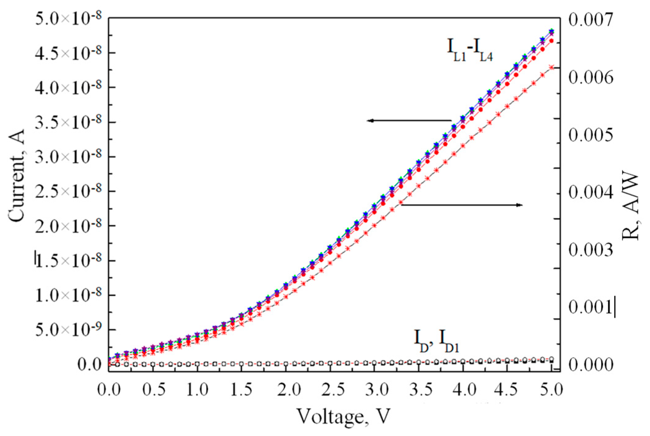
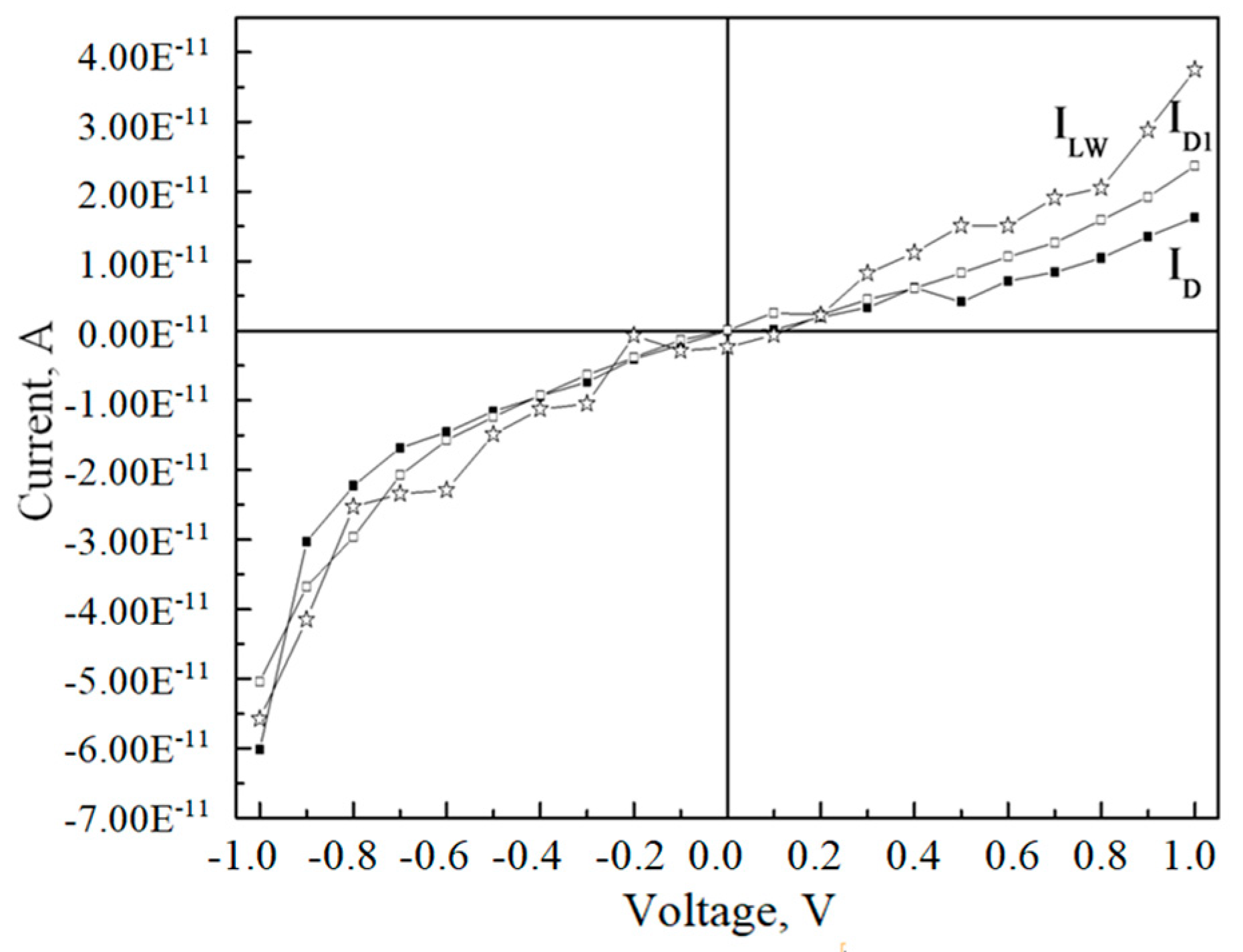
4.2. Electrical and Photoelectric Characteristics of Ga2O3/ZnGeP2 Structures after Annealing

Annealing leads to a significant change in the characteristics of Ga2O3/ZnGeP2 structures: direct currents are observed at positive voltages on the Pt electrode; dark currents increase (Figure 11); and sensitivity to UV and IR radiation increases.
In structures with an annealed gallium oxide film, the sensitivity to UV and IR radiation increases; the photovoltaic effect is preserved; Voc decreases to (0.3–0.5) V and is fixed at positive voltages; and short-circuit current increases by three orders of magnitude: Isc = (1.0–1.5) × 10−6 A (Figure 12).
After annealing, the responsivity R to λ = 254 nm at all voltages increases by an order of magnitude; the maximum values of R are obtained at negative voltages on the Pt electrode (Figure 12); at V = 0 V, the specific detectivity of the structures is D* = 1 × 1012 cm × Hg0.5 × W−1.
Lasers with wavelengths of 808 and 1064 nm and powers of 500 and 100 mW, respectively, were used as a source of IR radiation. Figure 10 shows the dark I-V characteristics and the light ones under λ = 808 nm (Figure 13a) and 1064 nm (Figure 13b) illumination.
Samples with an annealed Ga2O3 film have a photovoltaic effect under IR illumination, and the open-circuit voltage is observed at positive values of V. Under λ = 808 nm illumination with P = 500 mW, the open-circuit voltage Voc = (0.57–0.60) V and current Isc = 0.12 mA (Figure 11a) are recorded. Thus, the results from above show these structures can function without an external power source, making it, therefore, a self-powered device, which has potentially important applications such as secure ultraviolet communication and space detection.
It can be assumed that the sensitivity of the Ga2O3/ZnGeP2 structures to IR radiation with the annealed Ga2O3 film is due to the high transmittance T. However, the spectral dependences of T measured before and after annealing (Figure 14) refute this hypothesis. The question remains open, and research in this direction continues.

5. Conclusions

The electrical and photoelectric characteristics of Ga2O3/ZnGeP2 hetero-structures obtained by RF magnetron sputtering Ga2O3 (99.99%) target on polished ZnGeP2 substrates are studied. The samples are sensitive to UV radiation with λ = 254 nm and are able to work as self-powered detectors of short-wave radiation. Structures with Ga2O3 film not annealed at 400 °C show weak sensitivity to long-wave radiation, including the near-IR range (λ = 808 and 1064 nm). Annealing of the oxide film in the air (400 °C, 30 min) leads to an increase in the sensitivity of hetero-structures in both the UV and IR ranges. These structures can be used as radiation detectors in the IR range with the ability to operate as self-powered devices.

Author Contributions

Conceptualization, V.K. (Vera Kalygina) and S.P.; methodology, S.P., M.Z. and N.Y.; software, E.S., V.K. (Vladimir Kuznetsov) and H.B.; validation, A.L. and A.K.; formal analysis, B.K., B.K. and V.O.; investigation, M.Z., S.P. and P.Y.; resources, V.K. (Victor Kopiev) data curation, E.S. and M.Z.; writing—original draft preparation, A.L.; writing—review and editing, A.L. and H.B.; visualization S.P.; supervision V.K. (Vera Kalygina) and S.P.; project administration, V.K. (Vera Kalygina); funding acquisition, N.Y. All authors have read and agreed to the published version of the manuscript.

Funding

This study was supported by the Tomsk State University Development Program (Priority 2030).

Institutional Review Board Statement

Not applicable.

Informed Consent Statement

Not applicable.

Data Availability Statement

Not applicable.

Conflicts of Interest

The authors declare no conflict of interest. The funders had no role in the design of the study; in the collection, analyses, or interpretation of data; in the writing of the manuscript, or in the decision to publish the results.

References

  1. Kitaeva, G.K. Terahertz generation by means of optical lasers. Laser Phys. Lett. 2008, 5, 559–576. [Google Scholar] [CrossRef]
  2. Grigoreva, V.S.; Prochukhan, V.D.; Rud, Y.V.; Yakovenko, A.A. Some electrical properties of high-resistance ZnGeP2 single crystals. Phys. Status Solidi (a) 1973, 17, K69–K73. [Google Scholar] [CrossRef]
  3. Carnio, B.; Greig, S.; Firby, C.; Zawilski, K.; Schunemann, P.; Elezzabi, A. Terahertz electro-optic detection using a ⟨012⟩-cut chalcopyrite ZnGeP2 crystal. Appl. Phys. Lett. 2016, 108, 261109. [Google Scholar] [CrossRef]
  4. Barnoski, M. In the Integral Opticus/m. Barnoski, Ten, J. Goel et al. // In Order. M. Barnosky; Per. with English. in Order. T.A. Shmaonova; Mir: Moscow, Russia, 1977. [Google Scholar]
  5. Brudnyĭ, V.N.; Voevodin, V.G.; Grinyaev, S.N. Deep levels of intrinsic point defects and the nature of “anomalous” optical absorption in ZnGeP2. Phys. Solid State 2006, 48, 1949–1961. [Google Scholar] [CrossRef]
  6. Pearton, S.J.; Yang, J.; Cary, P.H.; Ren, F.; Kim, J.; Tadjer, M.J.; Mastro, M.A. A review of Ga2O3 materials, processing, and devices. Appl. Phys. Rev. 2018, 5, 011301. [Google Scholar] [CrossRef]
  7. Lin, C.-H.; Lee, C.-T. Ga2O3-based solar-blind deep ultraviolet light-emitting diodes. J. Lumin. 2020, 224, 117326. [Google Scholar] [CrossRef]
  8. Roy, R.; Hill, V.G.; Osborn, E.F. Polymorphism of Ga2O3 and the system Ga2O3–H2O. J. Am. Chem. Soc. 1952, 74, 719–722. [Google Scholar] [CrossRef]
  9. Zhang, D.; Dong, S. Challenges in band alignment between semiconducting materials: A case of rutile and anatase TiO2. Prog. Nat. Sci. Mater. Int. 2019, 29, 277–284. [Google Scholar] [CrossRef]
  10. Zhang, Z.; Farzana, E.; Arehart, A.R.; Ringel, S.A. Deep level defects throughout the bandgap of (010) β-Ga2O3 detected by optically and thermally stimulated defect spectroscopy. Appl. Phys. Lett. 2016, 108, 052105. [Google Scholar] [CrossRef]
  11. Boyd, G.D.; Beuhler, E.; Stortz, F.G. Linear and nonlinear optical properties of ZnGeP2 and CdSe. Appl. Phys. Lett. 1971, 18, 301–304. [Google Scholar] [CrossRef]
  12. Romanovskii, O.; Sadovnikov, S.A.; Kharchenko, O.V.; Yakovlev, S.V. Development of near/mid IR differential absorption OPO lidar system for remote gas analysis of the atmosphere. In Proceedings of the Remote Sensing of Clouds and the Atmosphere XXIV, Strasbourg, France, 9–11 September 2019; Volume 11152, pp. 236–243. [Google Scholar]
  13. Lv, Z.; Shen, Y.; Zong, N.; Bian, Q.; Wang, E.-P.; Chang, J.-Q.; Bo, Y.; Cui, D.-F.; Peng, Q.-J. 1.53 W all-solid-state nanosecond pulsed mid-infrared laser at 6.45 µm. Opt. Lett. 2022, 47, 1359. [Google Scholar] [CrossRef] [PubMed]
  14. Wang, X.; Chen, Z.; Guo, D.; Zhang, X.; Wu, Z.; Li, P.; Tang, W. Optimizing the performance of a β-Ga2O3 solar-blind UV photodetector by compromising between photoabsorption and electric field distribution. Opt. Mater. Express 2018, 8, 2918–2927. [Google Scholar] [CrossRef]
  15. Li, Z.; An, Z.; Xu, Y.; Cheng, Y.; Cheng, Y.; Chen, D.; Feng, Q.; Xu, S.; Zhang, J.; Zhang, C.; et al. Improving the production of high-performance solarblind b-Ga2O3 photodetectors by controlling the growth pressure. J. Mater. Sci. 2019, 54, 10335–10345. [Google Scholar] [CrossRef]
  16. Lia, M.-Q.; Yanga, N.; Wanga, G.-G.; Zhanga, H.-Y.; Hana, J.-C. Highly preferred orientation of Ga2O3 films sputtered on SiC substrates for deep UV photodetector application. Appl. Surf. Sci. 2019, 471, 694–702. [Google Scholar] [CrossRef]
  17. Kalygina, V.; Vishnikina, V.; Petrova, Y.; Prudaev, I.; Yaskevich, T. Photovoltaic characteristics of structures metal-Ga2O3-GaAs. Phys. Technol. Semicond. 2015, 49, 357–363. [Google Scholar]
  18. Yu, J.; Lou, J.; Wang, Z.; Ji, S.; Chen, J.; Yu, M.; Peng, B.; Hu, Y.; Yuan, L.; Zhang, Y.; et al. Surface modification of β-Ga2O3 layer using Pt nanoparticles for improved deep UV photodetector performance. J. Alloys Compd. 2021, 872, 159508. [Google Scholar] [CrossRef]
  19. Hou, X.; Zou, Y.; Ding, M.; Qin, Y.; Zhang, Z.; Ma, X.; Tan, P.; Yu, S.; Zhou, X.; Zhao, X.; et al. Review of polymorphous Ga2O3 materials and their solar-blind photodetector applications. J. Phys. D Appl. Phys. 2020, 54, 043001. [Google Scholar] [CrossRef]
Figure 1. Photograph of a wire-cutting machine.
Crystals 13 01203 g001
Figure 2. Photograph of polished ZGP plates glued to a faceplate.
Crystals 13 01203 g002
Figure 3. Schematic of device structure.
Crystals 13 01203 g003
Figure 4. X-ray diffraction analysis of gallium oxide film on the ZnGeP2 substrate.
Crystals 13 01203 g004
Figure 5. The schematic band diagram of the Ga2O3/ZnGeP2 hetero-junction.
Crystals 13 01203 g005
Figure 6. Current–voltage characteristics of the sample: (a) dark current (ID); (b) dark currents (ID, ID1) and under UV continuous illumination (IL1–IL5); dark current measured immediately after turning off the UV is indicated as ID1.
Crystals 13 01203 g006
Figure 7. Dependencies of dark currents before (ID) and after (ID1) UV illumination; currents under UV continuous illumination (IL1–IL4) and response R on voltage.
Crystals 13 01203 g007
Figure 8. Dark I-V characteristics of the photodetector before (ID) and after (ID1) 254 nm illumination; I-V characteristics during white light illumination with power of 3 × 10⁻³ W (ILW).
Crystals 13 01203 g008
Figure 9. Dependence of specific detectivity D* on voltage.
Crystals 13 01203 g009
Figure 10. Time profile of the current when switching on/off the radiation with λ = 254 nm and V = 1 V (a); start and end of a single pulse on a more detailed scale (b).
Crystals 13 01203 g010
Figure 11. Dependences of dark currents of samples without (ID) and after annealing (ID ann) on voltage.
Crystals 13 01203 g011
Figure 12. Dependences of dark (ID), light I-V characteristics (IL1–IL4), responsivity R of Ga2O3/ZnGeP2 structures at λ = 254 nm on voltage.
Crystals 13 01203 g012
Figure 13. Dependences of dark (ID) and light I-V characteristics of Ga2O3/ZnGeP2 structure on voltage during illuminating: with λ = 808 nm (P = 500 mW) (a); with λ = 1064 nm (P = 100 mW) (b).
Crystals 13 01203 g013
Figure 14. Transmission (T) spectra of Ga2O3 film without and after annealing.
Crystals 13 01203 g014
Table 1. Charge carrier concentration (p), mobility (Up), and acceptor impurity activation energy (Ea) for various ZnGeP2 samples.
Doping Impurity Impurity
Action
P
(cm−3)
Up
(cm2/V s)
Ea
(eV)
--1.5 × 1010600.65
Auinactive2.5 × 1010300.65
Cuinactive1.0 × 101013-
Seacceptor2.5 × 10140.50.4
Gaacceptor8.7 × 10160.180.31
Inacceptor1.4 × 10160.13-
Disclaimer/Publisher’s Note: The statements, opinions and data contained in all publications are solely those of the individual author(s) and contributor(s) and not of MDPI and/or the editor(s). MDPI and/or the editor(s) disclaim responsibility for any injury to people or property resulting from any ideas, methods, instructions or products referred to in the content.

