
Progress in Ammonothermal Crystal Growth of Gallium Nitride from 2017–2023: Process, Defects and Devices


Abstract
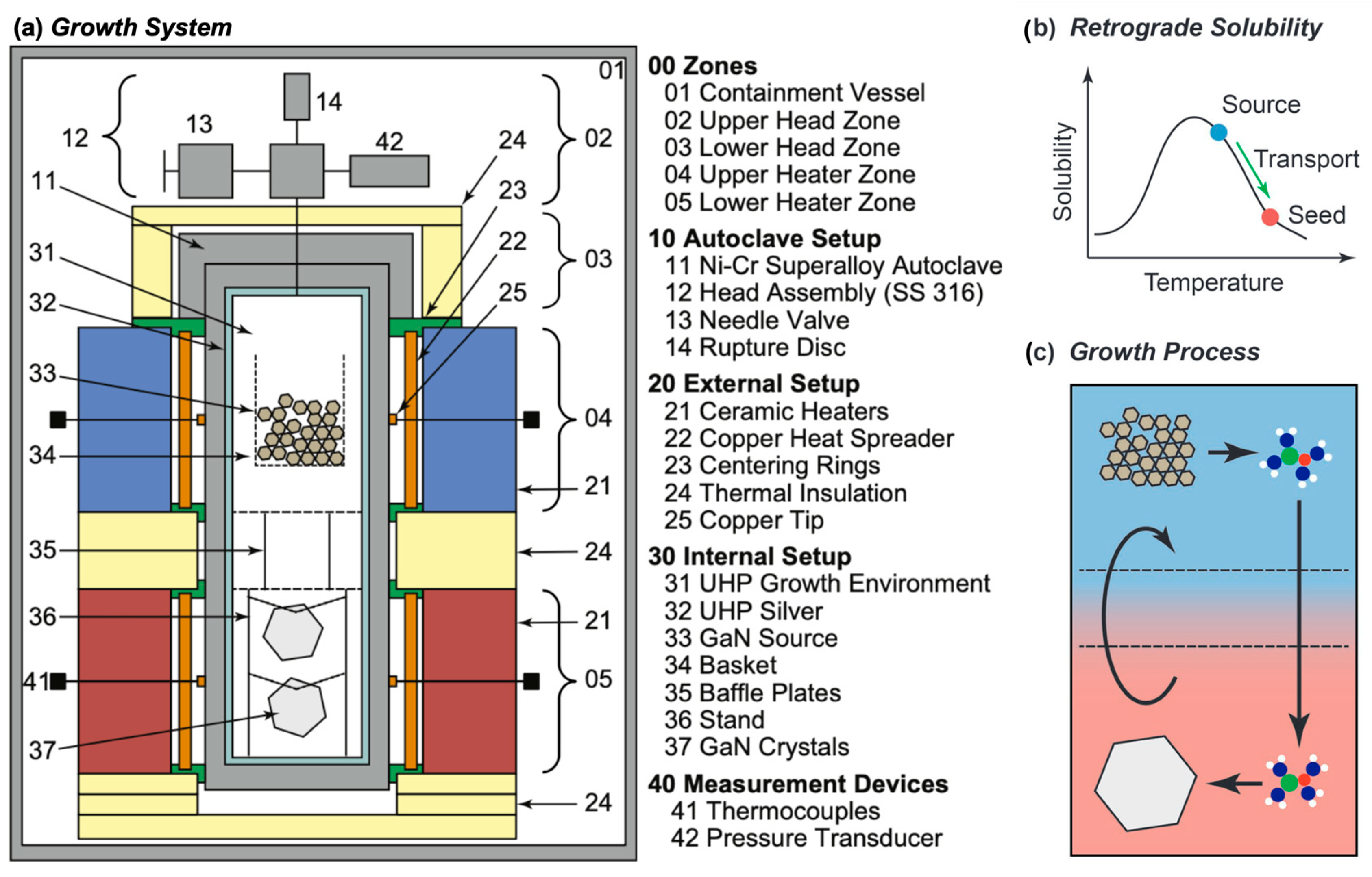
1. Introduction
2. Growth Methods and Technology
2.1. Progress in Growth Methods
2.2. In Situ Measurements of Ammonothermal Growth
3. Characterization Methods and GaN Material Properties
3.1. Structural Defects
3.2. Doping
3.3. Point Defects and Impurities
4. Device Performance Results
5. Conclusions
Author Contributions
Funding
Data Availability Statement
Conflicts of Interest
References
- Maruska, H.P.; Tietjen, J.J. The Preparation and Properties of Vapor-Deposited Single-Crystal GaN. Appl. Phys. Lett. 1969, 15, 327. [Google Scholar] [CrossRef]
- Nakamura, S.; Fasol, G. The Blue Laser Diode—GaN-Based Light Emitters and Lasers; Springer: Berlin, Germany, 1997; ISBN 987-3-662-03464-4S. [Google Scholar]
- Yoshida, T.; Oshima, Y.; Watanabe, K.; Tsuchiya, T.; Mishima, T. Ultrahigh-speed growth of GaN by hydride vapor phase epitaxy. Phys. Status Solidi 2011, 8, 2110–2112. [Google Scholar] [CrossRef]
- Kucharski, R.; Sochacki, T.; Lucznik, B.; Amilusik, M.; Grabianska, K.; Iwinska, M.; Bockowski, M. Ammonothermal and HVPE Bulk Growth of GaN. In Wide Bandgap Semiconductors for Power Electronics: Materials, Devices, Applications; Wellmann, P., Ohtani, N., Rupp, R., Eds.; Wiley-VCH GmbH: Weinheim, Germany, 2021; Chapter 18. [Google Scholar] [CrossRef]
- Baliga, B.J. Gallium nitride devices for power electronic applications. Semicond. Sci. Technol. 2013, 28, 074011. [Google Scholar] [CrossRef]
- Marino, F.A.; Faralli, N.; Ferry, D.K.; Goodnick, S.M.; Saraniti, M. Figures of merit in high-frequency and high-power GaN HEMTs. J. Phys. Conf. Ser. 2009, 193, 012040. [Google Scholar] [CrossRef]
- Hickman, A.L.; Chaudhuri, R.; Bader, S.J.; Nomoto, K.; Li, L.; Hwang, J.C.; Xing, H.G.; Jena, D. Next generation electronics on the ultrawide-bandgap aluminum nitride platform. Semicond. Sci. Technol. 2021, 36, 044001. [Google Scholar] [CrossRef]
- Tsao, J.Y.; Chowdhury, S.; Hollis, M.A.; Jena, D.; Johnson, N.M.; Jones, K.A.; Kaplar, R.J.; Rajan, S.; Van de Walle, C.G.; Bellotti, E.; et al. Ultrawide-Bandgap Semiconductors: Research Opportunities and Challenges. Adv. Electron. Mat. 2018, 4, 1600501. [Google Scholar] [CrossRef]
- Mori, Y.; Imade, M.; Maruyama, M.; Yoshimura, M.; Yamane, H.; Kawamura, F.; Kawamura, T. Bulk Crystal Growth: Basic Techniques, and Growth Mechanisms and Dynamics. In Handbook of Crystal Growth, 2nd ed.; Rudolph, P., Ed.; Elsevier: Amsterdam, The Netherlands, 2015; pp. 505–533. [Google Scholar]
- Dwiliński, R.T.; Wysmolek, A.; Baranowski, J.M.; Kamińska, M.; Doradziński, R.M. GaN Synthesis by Ammonothermal Method. Acta Phys. Pol. 1995, 88, 833–836. [Google Scholar] [CrossRef]
- Ehrentraut, D.; Bockowski, M. High-Pressure, High-Temperature Solution Growth and Ammonothermal Synthesis of Gallium Nitride Crystals; Rudolph, P., Ed.; Elsevier: Amsterdam, The Netherlands, 2015; pp. 577–619. [Google Scholar] [CrossRef]
- Zhang, S.; Alt, N.S.; Schlücker, E.; Niewa, R. Novel alkali metal amidogallates as intermediates in ammonothermal GaN crystal growth. J. Cryst. Growth 2014, 403, 22–28. [Google Scholar] [CrossRef]
- Zhang, S.; Hintze, F.; Schnick, W.; Niewa, R. Intermediates in Ammonothermal GaN Crystal Growth under Ammonoacidic Conditions. Eur. J. Inorg. Chem. 2013, 2013, 5387–5399. [Google Scholar] [CrossRef]
- Meissner, E.; Niewa, R. (Eds.) Ammonothermal Synthesis and Crystal Growth of Nitrides; Springer Series in Materials Science; Springer International Publishing: Cham, Switzerland, 2021. [Google Scholar]
- Pimputkar, S.; Kawabata, S.; Speck, J.S.; Nakamura, S. Improved growth rates and purity of basic ammonothermal GaN. J. Cryst. Growth 2014, 403, 7–17. [Google Scholar] [CrossRef]
- Suihkonen, S.; Pimputkar, S.; Sintonen, S.; Tuomisto, F. Defects in Single Crystalline Ammonothermal Gallium Nitride. Adv. Electron. Mater. 2017, 3, 1600496. [Google Scholar] [CrossRef]
- Zając, M.; Kucharski, R.; Grabianska, K.; Gwardys-Bak, A.; Puchalski, A.; Wasik, D.; Litwin-Staszewska, E.; Piotrzkowski, R.; Domagala, J.Z.; Bockowski, M. Basic ammonothermal growth of Gallium Nitride—State of the art, challenges, perspectives. Prog. Cryst. Growth Charact. Mater. 2018, 64, 63–74. [Google Scholar] [CrossRef]
- Häusler, J.; Schnick, W. Ammonothermal Synthesis of Nitrides: Recent Developments and Future Perspectives. Chem. Eur. J. 2018, 24, 11864–11879. [Google Scholar] [CrossRef]
- Hertrampf, J.; Alt, N.S.A.; Schlücker, E.; Niewa, R. Three Solid Modifications of Ba[Ga(NH2)4]2: A Soluble Intermediate in Ammonothermal GaN Crystal Growth. Eur. J. Inorg. Chem. 2017, 2017, 902–909. [Google Scholar] [CrossRef]
- Xu, L.; Li, T.; Ren, G.; Su, X.; Gao, X.; Zheng, S.; Wang, H.; Xu, K. Study of lateral growth regions in ammonothermal c-plane GaN. J. Cryst. Growth 2020, 556, 125987. [Google Scholar] [CrossRef]
- Hashimoto, T.; Letts, E.R.; Key, D. Progress in Near-Equilibrium Ammonothermal (NEAT) Growth of GaN Substrates for GaN-on-GaN Semiconductor Devices. Crystals 2022, 12, 1085. [Google Scholar] [CrossRef]
- Pimputkar, S.; Speck, J.S.; Nakamura, S. Basic ammonothermal GaN growth in molybdenum capsules. J. Cryst. Growth 2016, 456, 15–20. [Google Scholar] [CrossRef]
- Jiang, W.; Ehrentraut, D.; Cook, J.; Kamber, D.S.; Pakalapati, R.T.; D’Evelyn, M.P. Transparent, conductive bulk GaN by high temperature ammonothermal growth. Phys. Status Solidi 2015, 252, 1069–1074. [Google Scholar] [CrossRef]
- Kurimoto, K.; Bao, Q.; Mikawa, Y.; Shima, K.; Ishiguro, T.; Chichibu, S.F. Low-pressure acidic ammonothermal growth of 2-inch-diameter nearly bowing-free bulk GaN crystals. Appl. Phys. Express 2022, 15, 055504. [Google Scholar] [CrossRef]
- Tomida, D.; Bao, Q.; Saito, M.; Osanai, R.; Shima, K.; Kojima, K.; Ishiguro, T.; Chichibu, S.F. Ammonothermal growth of 2 inch long GaN single crystals using an acidic NH 4 F mineralizer in a Ag-lined autoclave. Appl. Phys. Express 2020, 13, 055505. [Google Scholar] [CrossRef]
- Grabianska, K.; Kucharski, R.; Sochacki, T.; Weyher, J.L.; Iwinska, M.; Grzegory, I.; Bockowski, M. On Stress-Induced Polarization Effect in Ammonothermally Grown GaN Crystals. Crystals 2022, 12, 554. [Google Scholar] [CrossRef]
- Grabianska, K.; Kucharski, R.; Puchalski, A.; Sochacki, T.; Bockowski, M. Recent progress in basic ammonothermal GaN crystal growth. J. Cryst. Growth 2020, 547, 125804. [Google Scholar] [CrossRef]
- Grabianska, K.; Jaroszynski, P.; Sidor, A.; Bockowski, M.; Iwinska, M. GaN Single Crystalline Substrates by Ammonothermal and HVPE Methods for Electronic Devices. Electronics 2020, 9, 1342. [Google Scholar] [CrossRef]
- Kucharski, R.; Sochacki, T.; Lucznik, B.; Bockowski, M. Growth of bulk GaN crystals. J. Appl. Phys. 2020, 128, 050902. [Google Scholar] [CrossRef]
- Shim, J.B.; Kim, G.H.; Lee, Y.K. Basic ammonothermal growth of bulk GaN single crystal using sodium mineralizers. J. Cryst. Growth 2017, 478, 85–88. [Google Scholar] [CrossRef]
- Hertrampf, J.; Schlücker, E.; Gudat, D.; Niewa, R. Dissolved Intermediates in Ammonothermal Crystal Growth: Stepwise Condensation of [Ga(NH2)4]-toward GaN. Cryst. Growth Des. 2017, 17, 4855–4863. [Google Scholar] [CrossRef]
- Li, T.; Guoqiang Ren Yao, J.; Su, X.; Zheng, S.; Gao, X.; Xu, L.; Xu, K. Study of stress in ammonothermal non-polar and semi-polar GaN crystal grown on HVPE GaN seeds. J. Cryst. Growth 2019, 532, 125423. [Google Scholar] [CrossRef]
- Li, T.; Ren, G.; Su, X.; Yao, J.; Yan, Z.; Gao, X.; Xu, K. Growth behavior of ammonothermal GaN crystals grown on non-polar and semi-polar HVPE GaN seeds. Crystengcomm 2019, 21, 4874–4879. [Google Scholar] [CrossRef]
- Li, T.; Ren, G.; Su, X.; Xie, K.; Xia, Z.; Gao, X.; Wang, J.; Xu, K. Evolution of V-pits in the ammonothermal growth of GaN on HVPE-GaN seeds. Crystengcomm 2022, 24, 8525–8530. [Google Scholar] [CrossRef]
- Griffiths, S.; Pimputkar, S.; Kearns, J.; Malkowski, T.F.; Doherty, M.F.; Speck, J.S.; Nakamura, S. Growth Kinetics of Basic Ammonothermal Gallium Nitride Crystals. J. Cryst. Growth 2018, 501, 74–80. [Google Scholar] [CrossRef]
- Schimmel, S.; Duchstein, P.; Steigerwald, T.G.; Kimmel, A.-C.L.; Schlücker, E.; Zahn, D.; Niewa, R.; Wellmann, P. In situ X-ray monitoring of transport and chemistry of Ga-containing intermediates under ammonothermal growth conditions of GaN. J. Cryst. Growth 2018, 498, 214–223. [Google Scholar] [CrossRef]
- Schimmel, S.; Salamon, M.; Tomida, D.; Neumeier, S.; Ishiguro, T.; Honda, Y.; Chichibu, S.F.; Amano, H. High-Energy Computed Tomography as a Prospective Tool for In Situ Monitoring of Mass Transfer Processes inside High-Pressure Reactors—A Case Study on Ammonothermal Bulk Crystal Growth of Nitrides including GaN. Materials 2022, 15, 6165. [Google Scholar] [CrossRef] [PubMed]
- Schimmel, S.; Tomida, D.; Ishiguro, T.; Honda, Y.; Chichibu, S.; Amano, H. Numerical Simulation of Ammonothermal Crystal Growth of GaN—Current State, Challenges, and Prospects. Crystals 2021, 11, 356. [Google Scholar] [CrossRef]
- Han, P.; Gao, B.; Song, B.; Yu, Y.; Tang, X. Improving the GaN Growth Rate by Optimizing the Nutrient Basket Geometry in an Ammonothermal System Based on Numerical Simulation. ACS Omega 2022, 7, 9359–9368. [Google Scholar] [CrossRef] [PubMed]
- Schimmel, S.; Tomida, D.; Ishiguro, T.; Honda, Y.; Chichibu, S.F.; Amano, H. Temperature Field, Flow Field, and Temporal Fluctuations Thereof in Ammonothermal Growth of Bulk GaN—Transition from Dissolution Stage to Growth Stage Conditions. Materials 2023, 16, 2016. [Google Scholar] [CrossRef] [PubMed]
- Malkowski, T.F.; Pimputkar, S.; Speck, J.S.; DenBaars, S.P.; Nakamura, S. Acidic ammonothermal growth of gallium nitride in a liner-free molybdenum alloy autoclave. J. Cryst. Growth 2016, 456, 21–26. [Google Scholar] [CrossRef]
- Malkowski, T.F.; Speck, J.S.; DenBaars, S.P.; Nakamura, S. An exploratory study of acidic ammonothermal growth in a TZM autoclave at high temperatures. J. Cryst. Growth 2018, 499, 85–89. [Google Scholar] [CrossRef]
- Holmi, J.T.; Bairamov, B.H.; Suihkonen, S.; Lipsanen, H. Identifying threading dislocation types in ammonothermally grown bulk α-GaN by confocal Raman 3-D imaging of volumetric stress distribution. J. Cryst. Growth 2018, 499, 47–54. [Google Scholar] [CrossRef]
- Liu, Y.; Raghothamachar, B.; Peng, H.; Ailihumaer, T.; Dudley, M.; Collazo, R.; Tweedie, J.; Sitar, Z.; Shahedipour-Sandvik, F.S.; Jones, K.A.; et al. Synchrotron X-ray topography characterization of high quality ammonothermal-grown gallium nitride substrates. J. Cryst. Growth 2020, 551, 125903. [Google Scholar] [CrossRef]
- Liu, Y.; Chen, Z.; Hu, S.; Peng, H.; Cheng, Q.; Rahothamachar, B.; Dudley, M. Strain mapping of GaN substrates and epitaxial layers used for power electronic devices by synchrotron X-ray rocking curve topography. J. Cryst. Growth 2022, 583, 126559. [Google Scholar] [CrossRef]
- Kirste, L.; Grabianska, K.; Kucharski, R.; Sochacki, T.; Lucznik, B.; Bockowski, M. Structural Analysis of Low Defect Ammonothermally Grown GaN Wafers by Borrmann Effect X-ray Topography. Materials 2021, 14, 5472. [Google Scholar] [CrossRef] [PubMed]
- Stoddard, N. Methods and Apparatus for Manufacturing Monocrystalline Cast Silicon and Monocrystalline Cast Silicon Bodies for Photovoltaics. U.S. Patent 8628614B2, 14 January 2014. [Google Scholar]
- Stoddard, N. Seed Layers and Process of Manufacturing Seed Layers. U.S. Patent 8882077B2, 11 November 2014. [Google Scholar]
- Kutsukake, K.; Usami, N.; Ohno, Y.; Tokumoto, Y.; Yonenaga, I. Mono-Like Silicon Growth Using Functional Grain Boundaries to Limit Area of Multicrystalline Grains. IEEE J. Photovolt. 2014, 4, 84–87. [Google Scholar] [CrossRef]
- Trempa, M.; Reimann, C.; Friedrich, J.; Muller, G.; Krause, A.; Sylla, L.; Richter, T. Influence of grain boundaries intentionally induced between seed plates on the defect generation in quasi-mono-crystalline silicon ingots. Cryst. Res. Technol. 2014, 50, 124–132. [Google Scholar] [CrossRef]
- Zhang, F.; Yu, X.; Liu, C.; Yuan, S.; Zhu, X.; Zhang, Z.; Huang, L.; Lei, Q.; Hu, D.; Yang, D. Designing functional Σ13 grain boundaries at seed junctions for high-quality cast quasi-single crystalline silicon. Sol. Energy Mater. Sol. Cells 2019, 200, 109985. [Google Scholar] [CrossRef]
- Schubert, M.; Schindler, F.; Benick, J.; Riepe, S.; Krenckel, P.; Richter, A.; Muller, R.; Hammann, B.; Nold, S. The potential of cast silicon. Sol. Energy Mater. Sol. Cells 2021, 219, 110789. [Google Scholar] [CrossRef]
- Hashimoto, T.; Letts, E.R.; Key, D.; Jordan, B. Two inch GaN substrates fabricated by the near equilibrium ammonothermal (NEAT) method. Jpn J. Appl. Phys. 2019, 58, SC1005. [Google Scholar] [CrossRef]
- Hashimoto, T.; Letts, E.R.; Key, D.; Jordan, B.; Shang, E. GaN Substrate development through the near equilibrium ammonothermal (NEAT) method and its application to higher performance GaN-based devices. In Proceedings of the SPIE Quantum Sensing and Nano Electronics and Photonics XVI, San Francisco, CA, USA, 3–7 February 2019; p. 10926. [Google Scholar]
- Tomida, D.; Bao, Q.; Saito, M.; Kurimoto, K.; Sato, F.; Ishiguro, T.; Chichibu, S.F. Effects of extra metals added in an autoclave during acidic ammonothermal growth of m-plane GaN single crystals using an NH4F mineralizer. Appl. Phys. Express 2018, 11, 091002. [Google Scholar] [CrossRef]
- Heikkinen, T.; Pavlov, J.; Ceponis, T.; Gaubas, E.; Zajac, M.; Tuomisto, F. Effect of Mn and Mg dopants on vacancy defect formation in ammonothermal GaN. J. Cryst. Growth 2020, 547, 125803. [Google Scholar] [CrossRef]
- Zajac, M.; Konczewicz, L.; Litwin-Staszewska, E.; Iwinska, M.; Kucharski, R.; Juillaguet, S.; Contreras, S. P-type conductivity in GaN:Zn monocrystals grown by ammonothermal method. J. Appl. Phys. 2021, 129, 135702. [Google Scholar] [CrossRef]
- Amilusik, M.; Sohacki, T.; Fijalkowski, M.; Lucznik, B.; Iwinska, M.; Sidor, A.; Teisseyre, H.; Domagala, J.; Grzegory, I.; Bockowski, M. Homoepitaxial growth by halide vapor phase epitaxy of semi-polar GaN on ammonothermal seeds. Jpn J. Appl. Phys. 2019, 58, SC1030. [Google Scholar] [CrossRef]
- Reschikov, M.A.; Demchenko, D.O.; Ye, D.; Andrieiev, O.; Vorobiov, M.; Grabianska, K.; Zajac, M.; Nita, P.; Iwinska, M.; Bockowski, M.; et al. The effect of annealing on photoluminescence from defects in ammonothermal GaN. J. Appl. Phys. 2022, 131, 035704. [Google Scholar] [CrossRef]
- Jiang, W.; Nolan, M.; Ehrentraut, D.; D’Evelyn, M.P. Electrical and optical properties of gallium vacancy complexes in ammonothermal GaN. Appl. Phys. Express 2017, 10, 075506. [Google Scholar] [CrossRef]
- Suihkonen, S.; Pimputkar, S.; Speck, J.S.; Nakamura, S. Infrared absorption of hydrogen-related defects in ammonothermal GaN. Appl. Phys. Lett. 2016, 108, 202105. [Google Scholar] [CrossRef]
- Tuomisto, F.; Kuittinen, T.; Zając, M.; Doradziński, R.M.; Wasik, D. Vacancy–hydrogen complexes in ammonothermal GaN. J. Cryst. Growth 2014, 403, 114–118. [Google Scholar] [CrossRef]
- Polyakov, A.Y.; Smirnov, N.B.; Shchemerov, I.V.; Gogova, D.; Tarelkin, S.A.; Lee, I.; Pearton, S.J. Electrical Properties of Bulk, Non-Polar, Semi-Insulating M-GaN Grown by the Ammonothermal Method. ECS J. Solid State Sci. Technol. 2018, 7, P260. [Google Scholar] [CrossRef]
- Chen, S.-W.H.; Wang, H.; Hu, C.; Chen, Y.; Wang, H. Vertical GaN-on-GaN PIN diodes fabricated on free-standing GaN wafer using an ammonothermal method. J. Alloy Compd. 2019, 804, 435–440. [Google Scholar] [CrossRef]
- Key, D.; Letts, E.; Tsou, C.; Ji, M.; Bakhtiary-Noodeh, M.; Detchprohm, T.; Shen, S.; Dupuis, R.; Hashimoto, T. Structural and Electrical Characterization of 2″ Ammonothermal Free-Standing GaN Wafers. Progress toward Pilot Production. Materials 2019, 12, 1925. [Google Scholar] [CrossRef]
- Taube, A.; Kaminski, M.; Tarenko, J.; Sadowski, O.; Ekielski, M.; Szerling, A.; Prystawko, P.; Bockowski, M.; Grzegory, I. High Breakdown Voltage and High Current Injection Vertical GaN-on-GaN p-n Diodes with Extremely Low On-Resistance Fabricated on Ammonothermally Grown Bulk GaN Substrates. IEEE Trans. Electron Devices 2022, 69, 6255–6259. [Google Scholar] [CrossRef]
- Talesara, V.; Zhang, Y.; Vangipuram, V.G.T.; Zhao, H.; Lu, W. Vertical GaN-on-GaN pn power diodes with Baliga figure of merit of 27 GW/cm2. Appl. Phys. Lett. 2023, 122, 123501. [Google Scholar] [CrossRef]


| Units | IIHP/NL3 | SixPoint | Tohoku/MCC | Soraa/Kyocera | Competition | |
|---|---|---|---|---|---|---|
| Method | Am-GaN-B | NEAT | SCAAT/LPAAT | SCoRA | HVPE | |
| Chemistry | Basic | Basic | Acidic | Acidic | GaCl3-NH3 | |
| Wafer Size | cm | 50–60 | 50–100 | 50–60 | 50 (2015) | 50–150 |
| Growth Rate | mm/day | 24–60 | 30 | 170–205 | 700 | 2400 |
| Temp. Range | deg. C | 400–750 | 450–600 | 550–625 | 650–800 | 900–1100 |
| Press. Range | MPa | 100–600 | 100–300 | 100–200 | 100–600 | Low |
| Oxygen | atoms/cm3 | 1018–2 × 10¹⁹ | 2–8 × 10¹⁸ | - | 1018 | 1017–1019 |
| DD | defects/cm2 | 103–5 × 10⁴ | 105 | 1–5 × 10⁴ | 105 | 5 × 10⁶–108 |
| Curvature | m | >20 | 20 | 1460 | >20 | 1–5 |
| Rocking Width | arcsec | <30 | 20–50 | 20–30 | <30 | 30–80 |
| Boule Thickness | mm | 3–4 | 1–3 | 2–3 | >2 | 3–4 |
| Crystals/run | # | 36 | 50 | - | - | 1 |
| Dislocation Method | Units | Confocal Raman | Synchrotron XRT | Defect Etching | CL | PL | Bevel Etching | Borrmann XRT | HR-XRD |
|---|---|---|---|---|---|---|---|---|---|
| Sample Area | mm2 | 0.0025 | 2500 | 0.25 | 2500 | 2500 | 0.25 | 2500 | 4 |
| Dislocation Typing? | Yes | Yes | No | No | No | Yes | Yes | No | |
| Destructive? | No | No | Yes | No | No | Yes | No | No | |
| In-line Potential? | No | No | No | Maybe | Yes | No | Yes | Yes | |
| Range Capability | Disl/cm2 | <106 | 102–106 | 102–5 × 10⁶ | - | - | - | <105 | >104 |
| Measurement Depth | Surface | Full Depth | Surface | Surface | Full Depth | Full Depth | Full Depth | Full Depth | |
| 3D Depth Contrast | mm | 2–25 | N/A | N/A | N/A | N/A | 5–400 | N/A | N/A |
| Element | Typical Range (atoms/cm3) | Amilusik Range (atoms/cm3) | Change |
|---|---|---|---|
| H | 1 × 10¹⁹ to 6 × 10²⁰ | 4 × 10¹⁸ to 5 × 10¹⁹ | Improvement |
| C | High 1016 to Low 1017 | 8 × 10¹⁶ to 1.5 × 10¹⁸ | Similar to worse |
| Si | Low 1018 | 1 × 10¹⁷ to 2 × 10¹⁸ | Similar |
| Na | 1 × 10¹⁶ to 1 × 10¹⁹ | 1 × 10¹⁶ to 7 × 10¹⁷ | Similar to better |
| Mg | High 1016 to Low 1017 | 5 × 10¹⁵ to 8 × 10¹⁷ (dopant) | Similar |
| Mn | 3 × 10¹⁶ to 2 × 10¹⁸ | 6 × 10¹⁵ to 1 × 10¹⁸ (dopant) | Similar |
| Fe | ~1016 to Low 1017 | 3 × 10¹⁵ to 2 × 10¹⁶ | Improvement |
| Zn | Not reported | 8 × 10¹⁶ to 2.5 × 10¹⁸ | N/A |
Disclaimer/Publisher’s Note: The statements, opinions and data contained in all publications are solely those of the individual author(s) and contributor(s) and not of MDPI and/or the editor(s). MDPI and/or the editor(s) disclaim responsibility for any injury to people or property resulting from any ideas, methods, instructions or products referred to in the content. |
© 2023 by the authors. Licensee MDPI, Basel, Switzerland. This article is an open access article distributed under the terms and conditions of the Creative Commons Attribution (CC BY) license (https://creativecommons.org/licenses/by/4.0/).
Share and Cite
Stoddard, N.; Pimputkar, S. Progress in Ammonothermal Crystal Growth of Gallium Nitride from 2017–2023: Process, Defects and Devices. Crystals 2023, 13, 1004. https://doi.org/10.3390/cryst13071004
Stoddard N, Pimputkar S. Progress in Ammonothermal Crystal Growth of Gallium Nitride from 2017–2023: Process, Defects and Devices. Crystals. 2023; 13(7):1004. https://doi.org/10.3390/cryst13071004
Chicago/Turabian StyleStoddard, Nathan, and Siddha Pimputkar. 2023. "Progress in Ammonothermal Crystal Growth of Gallium Nitride from 2017–2023: Process, Defects and Devices" Crystals 13, no. 7: 1004. https://doi.org/10.3390/cryst13071004
APA StyleStoddard, N., & Pimputkar, S. (2023). Progress in Ammonothermal Crystal Growth of Gallium Nitride from 2017–2023: Process, Defects and Devices. Crystals, 13(7), 1004. https://doi.org/10.3390/cryst13071004