Abstract
Optimized vertical heterojunction rectifiers with a diameter of 100 µm, consisting of sputter-deposited p-type NiO forming a p–n junction with thick (10 µm) Ga2O3 drift layers grown by halide vapor phase epitaxy (HVPE) on (001) Sn-doped (1019 cm−3) β-Ga2O3 substrates, exhibited breakdown voltages > 8 kV over large areas (>1 cm2). The key requirements were low drift layer doping concentrations (<1016 cm3), low power during the NiO deposition to avoid interfacial damage at the heterointerface and formation of a guard ring using extension of the NiO beyond the cathode metal contact. Breakdown still occurred at the contact periphery, suggesting that further optimization of the edge termination could produce even larger breakdown voltages. On-state resistances without substrate thinning were <10 mΩ·cm−2, leading to power figure-of-merits > 9 GW·cm−2. The devices showed an almost temperature-independent breakdown to 600 K. These results show the remarkable potential of NiO/Ga2O3 rectifiers for performance beyond the limits of both SiC and GaN. The important points to achieve the excellent performance were: (1) low drift doping concentration, (2) low power during the NiO deposition and (3) formation of a guard ring.
1. Introduction
The ultra-wide bandgap semiconductors with bandgaps > 4.5 eV include BN, diamond, AlN and Ga2O3. These materials have the potential for much higher voltage operation than the currently available SiC and GaN power devices, but with lower on-resistance and switching losses. Ga2O3 appears to be an attractive option because of the availability of low cost, large area crystals. The various polytypes of Ga2O3 are attracting attention for their potential application in power switching, solar-blind UV detectors and lateral transistors with enhanced two-dimensional electron gases densities. It is possible to grow bulk crystals of the stable monoclinic β-polymorph from the melt, which enables large-diameter, high-quality substrates for homoepitaxy with low manufacturing costs. The rhombohedral α-polymorph has the largest bandgap and is isomorphous with α-Al2O3, so it is grown on inexpensive sapphire substrates. The orthorhombic κ-polymorph possesses ferroelectric properties and large spontaneous electrical polarization.
Ga2O3 has a high critical electric field strength—at least 8 mV·cm−1. This allows for higher operating voltages and lower switching losses in power electronics. Ga2O3 devices switch faster than Si devices at the same voltage and current ratings. The large bandgap makes it promising for high temperatures and radiation environment applications. As a result, Ga2O3 is being considered for several power electronics applications, including inverters, motor drives and power supplies. There is particular interest in kV-class vertical rectifiers for use in electric vehicles and their charging infrastructure as well as power management systems for improved switching efficiency for next generation power grids and efficiently interfacing renewable energy sources with these grids [1,2,3,4]. Power conversion systems that convert electricity from one form to another comprise AC-to-AC, AC-to-DC, DC-to-AC and DC-to-DC converters, which are used to adjust the voltages and currents for specific applications. A typical example of an electric vehicle and its charging system requires these essential components of power switching and conditioning. A key aspect is the boost converter, which takes in an input voltage and outputs a higher voltage at the load terminals. The key to this operation is a power switch. The enhancement of the efficiency of these switches leads to a much higher efficiency conversion and also to improved system compactness.
One of the goals is to achieve a high-power figure of merit for power electronic devices, defined as (VB)2/RON where VB is the reverse breakdown voltage and RON− is the on-state resistance [1,2,3,4]. To achieve a high-power figure of merit, a rectifier must have a low drift layer concentration, with high electron mobility, as well as low RON, and optimized edge termination to prevent current crowding [1,5,6,7,8,9,10,11,12,13,14,15,16,17,18,19,20,21]. The breakdown voltage is larger for thicker drift layers, but this degrades on-resistance. To achieve a low Ron, a thin drift layer with high electron mobility is required. In addition, vertical geometry devices are desirable, because of their higher power conversion efficiency and absolute currents compared to lateral devices [1,3,4,5]. The expression for RON is , where ε is the permittivity, µ is the mobility and EC is the critical field for breakdown. The latter scales approximately as EG1.7. The critical field decreases with the drift layer doping and is doping-dependent at large thickness.
The lack of p-type doping options for Ga2O3 has led to the use of p-type oxides to form p–n heterojunctions with the n-type Ga2O3 [6,7,8,9,10,11,12,13,14]. The most successful has been NiO, deposited by sputtering. The forward current transport mechanism in such junctions is typically by recombination at low biases and trap-assisted tunneling at higher bias [10,21,22,23,24,25,26]. Promising rectifier performance has been reported with this approach [12,13,14,21,22,23,24,25,26,27,28,29,30,31,32,33,34,35,36,37,38,39], including VB > 8 kV, with a figure of merit of 13.2 GW·cm−2 [12]. The rationale for this current work is to use a p–n heterojunction to achieve a higher breakdown voltage than is possible with Schottky rectifiers.
Optimization of the heterojunction rectifier device structure is crucial to achieve both high VB and low RON, as well as providing management of the maximum electric fields within the structure to enhance further the device voltage blocking capability [40,41,42,43,44,45]. The design variables include the thickness and doping of the layers, doping in the drift layer and the use of the NiO as a guard ring by extending it beyond the metal cathode [46,47,48,49,50,51,52,53,54,55,56,57,58,59,60,61,62]. In this paper, we report an investigation of the uniformity of achieving high VB and low RON in heterojunction rectifiers, the effect of drift layer doping and the temperature dependence of the performance of NiO/Ga2O3 to 600 K.
2. Experimental Section
Vertical geometry Schottky rectifiers and NiO/Ga2O3 rectifiers were fabricated on the same wafers to compare the characteristics. The bilayer NiO thickness of 10/10 nm and the length of the NiO extension beyond the cathode contact (12 µm) to form guard rings were held constant. The epitaxial layer structures were purchased from Novel Crystal Technology, Japan. They consisted of a lightly doped drift layer on a conducting substrate. The drift region thickness was 10 µm, grown by halide vapor phase epitaxy (HVPE) on a (001) Sn-doped (1019 cm−3), β-Ga2O3 single crystal substrate. Both on-resistance and the breakdown voltage increase with the drift layer thickness, but breakdown voltage is a strong function of the epilayer doping and should be as low as possible.
Full area Ohmic contacts were made to the rear surface using Ti/Au deposited by e-beam evaporation and annealed at 550 °C for 180 s under N2. The front surface was cleaned by UV/Ozone exposure for 15 min. The NiO bilayer was deposited by rf (13.56 MHz) magnetron sputtering at 3mTorr. The hole concentration was adjusted using the Ar/O2 ratio and the structure was annealed at 300 °C under O2. The gas flow ratio controls the stoichiometry of the film and the concentration of point defects that define the effective carrier concentration. A very detailed report of the properties of NiO deposited on Ga2O3 has been given previously [63]. The layers are polycrystalline, but we have no information on the possible grain boundary effects on the device performance. Finally, a cathode contact of 20/80 nm Ni/Au (100 µm diameter) was deposited onto the NiO layer. The NiO was extended 12 µm beyond the contact metal to form a guard ring. C−2-V plots for the drift layer doping showed the carrier concentration of the drift layers varied from 8 × 10¹⁵ to 6.7 × 1015 cm−3. Figure 1 shows a schematic of the heterojunction devices fabricated. We also included Schottky rectifiers without the NiO in order to compare the performance of conventional and heterojunction rectifiers. We note that the NiO extension beyond the top contact was held constant at 12 µm to form a guard ring, which was determined by TCAD simulations to provide the best field mitigation.
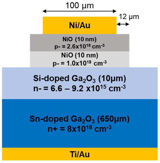
Figure 1.
Schematic of NiO heterojunction rectifiers fabricated on Ga2O3 substrate.
Characterization of the atomic structure of the NiO/β-Ga2O3 heterostructure was carried out using high-angle annular dark-field (HAADF) imaging in the scanning mode of transmission electron microscopy (STEM). For STEM studies, cross-section samples were prepared using a Thermo Scientific Helios G4 Cxe dual-beam plasma focused ion beam scanning electron microscope (PFIB-SEM). HAADF imaging in STEM was performed using a Thermo Scientific Themis Z equipped with a probe aberration corrector operated at the acceleration voltage of 200 kV.
The current density–voltage (J–V) characteristics were measured on a Tektronix 370-A curve tracer, 371-B curve and Agilent 4156C. For the highest reverse voltages, a Glassman power supply was employed. The reverse breakdown voltage was defined as the bias for a reverse current reaching 0.1 A·cm2. The high bias measurements were performed in Fluorinert atmosphere. The devices did not suffer permanent damage at this condition but increasing the voltage a further 50–200 V led to permanent failure through breakdown at the contact periphery. The on-resistance values were calculated assuming the current spreading length was 10 µm and a 45° spreading angle. We also subtracted the resistance of the cable, probe and chuck, which was around 10 Ohm. The drift layer doping was extracted from capacitance–voltage (C–V) data measured at 100 kHz. Photos of the setup have appeared previously [21,38].
3. Results
Figure 2a displays a HAADF-STEM image of the vertical rectifier near the junction between NiO and β-Ga2O3, imaged along the [00] projection with respect to the monoclinic β-Ga2O3 structure. The high-magnification HAADF-STEM image in Figure 2b from the red box in Figure 2a shows that the NiO/β-Ga2O3 interface is atomically abrupt. A 2 nm thick top layer of β-Ga2O3 shows diffuse image intensity of individual atomic columns which is likely due to the local atomic replacement resulting from the NiO sputtering process. However, the atomic structure retains as β-phase with no visible extended defects, indicating that the low-power sputtering process adopted in this study induces negligible structural damage at the surface of β-Ga2O3 compared to previous reports that used higher sputtering powers. Figure 2c,d shows a high-magnification HAADF-STEM image of β-Ga2O3 and a corresponding atomic model which reveal the [00] zone axis with the growth surface of (001).
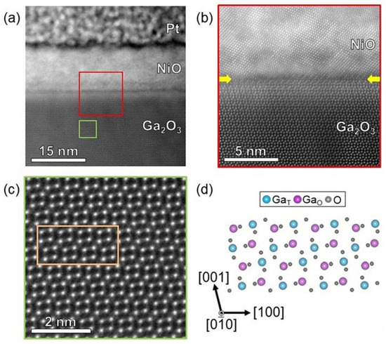
Figure 2.
(a) HAADF-STEM image of the vertical heterojunction rectifier near the NiO/β-Ga2O3 interface. (b) High-magnification HAADF-STEM of the NiO/β-Ga2O3 interface in the red box in (a) showing atomically abrupt interface marked with the yellow arrows. (c) HAADF-STEM image from the box in (a,d) atomic structure of β-Ga2O3 in the box in (c), the [] zone axis with the growth in (001) direction. Blue and purple circles in (d) represents Ga atoms with tetrahedral and octahedral coordination, respectively, while grey circles indicate oxygen. Note since the atomic number sensitive image contracts in HAADF-STEM images, only Ga atomic columns are seen in (c).
Figure 3 shows how important it is to have the lowest possible ion energy during the sputtering process in order to minimize the damage to the semiconductor surface. The top of Figure 3 shows the presence of a disordered region when using a power of 150 W, corresponding to a negative self-bias of 95–100 V on the powered electrode. By sharp contrast, when the power was lowered to 70 W, the bottom of Figure 3 shows that the disorder was significantly reduced. This rf sputtering power corresponded to a self-bias of 60–70 V, which reduced the corresponding ion energy incident on the surface and therefore reduced the ion-induced damage. We found this was crucial in achieving high breakdown voltages in the heterojunction rectifiers. The Ga2O3 surface was sensitive to disruption and under plasma etching conditions, the damage depth could reach over 100 nm unless careful attention was paid to the minimization of ion-induced damage.
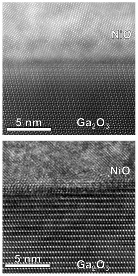
Figure 3.
Cross-sectional TEM images for the interfaces of NiO/Ga2O3 = heterojunctions with the NiO deposited at 150 W sputtering power(top) or 70 W (bottom). The top image was recorded along the [] zone axis bottom image was recorded along the [100] projection with respect to β-Ga2O3.
Figure 4 shows an optical image of the devices fabricated over an approximate 1 cm2 area. We measured 24 separate devices over this area to give an idea of uniformity. We focused on the 100 µm devices. The devices fell at the edge of the top contact due to field-induced breakdown. The rectifiers that failed often showed delamination of the epitaxial layer. There were also multiple crack lines observed along the [00] direction. The low thermal conductivity of Ga2O3 produced mechanical failure of the material along the natural cleavage planes. The concentration of heat in the lightly doped epitaxial layer relative to the heavily doped substrate led to differential thermal expansion and delamination of the epitaxial layer.
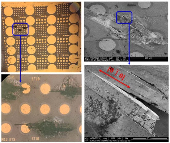
Figure 4.
Optical image of devices in a 1 cm2 area that was used to quantify uniformity of device parameters (top left). Devices tested to failure showed catastrophic breakdown at the contact periphery (bottom left) and delamination along crystal planes (right, top and bottom).
Figure 5 shows the collected C−2-V data from 24 locations. The drift layer doping varied in the range 6.6–9.2 × 1015 cm−2 over the 1 cm−2 area. This was outstanding uniformity from an HVPE growth cycle.
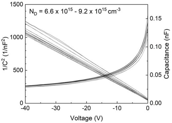
Figure 5.
C−2-V plots from 24 devices with a 1 × 1 cm2 area on the fabricated wafer.
Figure 6 shows a compilation of forward I–V characteristics from the 24 devices, along with the corresponding RON and on–off ratios. The former varied in the range 7.1–7.8 mΩ·cm2 and the on–off ratios were in the range from 4.8 × 10¹¹ to 2.9 × 10¹².The turn-on voltages were derived from the linear plots of forward current density as a function of voltage and are shown in Figure 7. These were tightly distributed in the range 2.1–2.2 V.
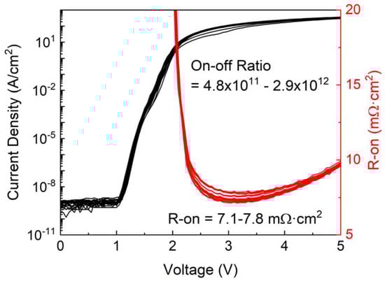
Figure 6.
Compilation of forward I–V characteristics from 24 devices measured over a 1 cm2 area. The corresponding range of RON and on–off ratios are also shown.
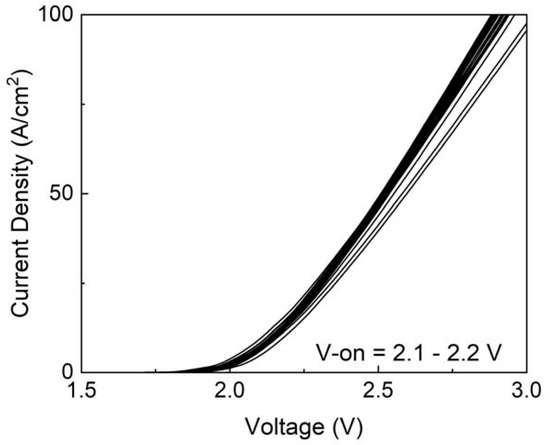
Figure 7.
Linear pots of J–V from which the forward turn-on voltages were calculated.
Figure 8 shows a collection of the reverse I–V characteristics from the 24 different devices measured. The distribution of the VB values, defined as the voltage where the reverse current reaches 0.1 A·cm−2, showed that most were >8 kV. By contrast, the Schottky rectifiers fabricated on the same regions had VB values of 1100–1500 V, showing the advantage of using the heterojunction approach. When the drift layer doping was higher (8 × 1015 cm−3), the VB values were centered around 7.5 kV, confirming the importance of low background carrier concentration. Typically, the Schottky rectifier results in the literature are in the range 800–2 kV for planar devices at these epi thicknesses, but there is a strong variation from wafer-to-wafer and the position on the wafer due to existing uniformity issues.
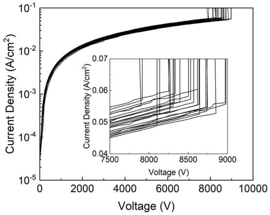
Figure 8.
Reverse current density-voltage plots for heterojunction rectifiers fabricated over 1 cm2 area. The inset shows an expanded view of the breakdown region.
A more detailed view is shown in the inset of Figure 8, with 22 of the 24 devices showing breakdown > 8 kV. The maximum VB was 8.9 kV. These results emphasized the excellent uniformity of the starting epitaxial layers. When breakdown occurred, it was still at the contact periphery, with delamination of the epilayers occurring, as shown in the images in Figure 4 (left bottom and right, top and bottom). This indicates that field crowding at the edge of the contact remains an issue.
The reverse current densities at −100 V are shown in Figure 9 for the population of devices measured. Again, the spatial variation was relatively small, with all devices exhibiting values <10−7 A·cm−2.
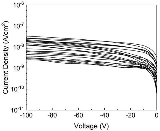
Figure 9.
Reverse J-V characteristics to −100 V from 24 devices.
We also measured the temperature dependence of VB. Figure 10 shows that for the heterojunction devices, there was a relatively small degradation in VB to 600 K. This was in contrast to the case of the Schottky rectifiers fabricated on the same wafers, where the breakdown voltage exhibited a large negative temperature coefficient. We also observed that the RON increased with temperature, due to the deterioration of mobility. In Ga2O3, the ionization energy of the n-type dopants is small, so increased ionization does not reduce the RON. Note that in the figure we have shown the range of values obtained at 300 K; we took the highest value for discussion of the temperature dependence.
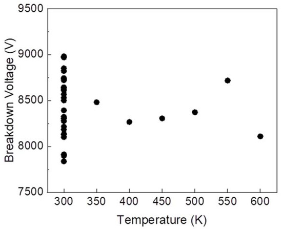
Figure 10.
Temperature dependence of breakdown voltage in heterojunction rectifiers. The range of values at 300 K is also shown.
To place this work in context, Figure 11 shows a compilation of the literature values for on-resistance as a function of the breakdown voltage for the rectifiers measured at room temperature, along with the theoretical values for SiC, GaN and Ga2O3. The bar indicated in red shows the values we obtained in this work for the breakdown voltage of the NiO/GaO3 rectifiers as a function of temperature from 300 = −600 K. Note that the heterojunction rectifiers have much larger breakdown voltages than the Schottky diodes. Since this was the first study of the temperature dependence in the performance of the heterojunction rectifiers, more work is needed to understand the results, but the large bandgaps of the NiO and Ga2O3 are conducive to high temperature operation. In addition, while impact ionization should have a positive temperature coefficient, that is not the dominant breakdown mechanism in the current state-of-the art material, where the impact ionization of deep acceptors has been identified as the dominant mechanism [64,65].
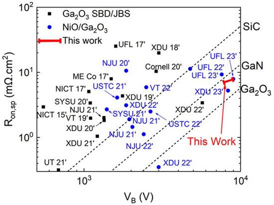
Figure 11.
Compilation of Ron versus VB of conventional Schottky Barrier Diodes and Junction Barrier Schottky diodes (SBD/JBS) and NiO/Ga2O3 heterojunction small area rectifiers reported in the literature. The results from this manuscript in the temperature range 300–600 K are shown in red as the bar. The other results are all from room temperature measurements.
4. Summary and Conclusions
The power figure of merits reported here were around 26% of the theoretical maximum for Ga2O3 assuming the 1D punch-through breakdown mechanism; it is anticipated that the continued reduction in defect density could enhance the future performance closer to this maximum. This is because bulk Ga2O3 crystals are known to have internal planar defects, i.e., plate-like voids and stacking faults, and it is known that higher dislocation densities lead to higher leakage currents in Ga2O3 rectifiers. The dislocations can act as recombination centers for electrons and holes, leading to an increased probability of carrier recombination and subsequent leakage current and hence lower breakdown voltage. The killer defect density was still quite high (10~100/cm2), caused by a specific powder mainly generated during epitaxial deposition. One possible approach to removing these is to soak the sample in 100 °C 11 M KOH for 30 min to remove it. It should be an important step for fabricating larger diodes. The difficulty of having a thicker epilayer is due to the formation of cracks that occur during longer growth times.
The NiO/Ga2O3 heterojunction rectifier is potentially an ideal structure for high-voltage and high-power applications, where it can offer better efficiency and reduced energy losses compared to traditional semiconductors. The wide bandgap of both NiO (~3.9 eV) and β-Ga2O3 (4.8 eV) also makes the power rectifiers from this heterojunction attractive for high-temperature applications. The heterojunction produced breakdown voltages far more than the Schottky rectifiers fabricated on the same wafer and confirmed that the NiO can act as both the p-layer and guard ring material. For a particular drift layer doping, there is a saturation thickness beyond which VB does not increase further. If the doping level is reduced, the saturation thickness increases. In our case, we observed a clear increase in the VB with reduced drift layer doping. It was also important to minimize the RON to limit the power lost due to Joule heating. It should also be remembered that the RON is not necessarily the heterojunction rectifiers actual resistance in the on-state, where the conduction mechanism is dominated by the minority carrier diffusion of minority carriers. The RON normally reported is the unipolar drift resistance, which is usually smaller than the diffusion resistance.
What are the implications for the expected critical breakdown field of Ga2O3? This is generally reported as ~8 mV·cm−1, but there is considerable uncertainty around this value, since most calculations assume breakdown occurs when the applied electric field and depletion width are sufficiently high to create infinite charge multiplication. This inherently assumes that the impact ionization is the breakdown mechanism, but this has never been experimentally verified in Ga2O3 and in any case, the impact ionization coefficients have not been measured either. The performance of NiO/β-Ga2O3 rectifiers deteriorates only slightly with temperature up to 600 K. Thermal-induced failure of rectifiers can occur due to plastic crystallographic deformation near the epi–substrate interface, and electrical breakdown is still dominated by field crowding at the contact periphery [66].
The important points to achieve high device performance were: (1) low drift doping concentration, (2) low power during the NiO deposition and (3) formation of a guard ring. The functional dependence of the first of these is well understood, but it has not been widely understood that the surface of Ga2O3 is quite sensitive too ion-induced damage, hence, the NiO sputter depiction conditions must be optimized. Finally, field mitigation at the edge of the top contact is still crucial, hence, the NiO extension beyond this contact is important.
The excellent performance reported here make the NiO/Ga2O3 power rectifiers promising for high-power and high-temperature applications such as electric vehicles, power electronics and aerospace.
Author Contributions
All contributed equally to all aspects of paper. All authors have read and agreed to the published version of the manuscript.
Funding
The research was funded by the Department of the Defense, Defense Threat Reduction Agency under award HDTRA1-20-2-0002. The work at UF was also supported by NSF DMR 1856662.
Data Availability Statement
The data that supports the findings of this study are available within the article.
Acknowledgments
The work at UF was performed as part of Interaction of Ionizing Radiation with Matter University Research Alliance (IIRM-URA), sponsored by the Department of the Defense, Defense Threat Reduction Agency under award HDTRA1-20-2-0002. The content of the information does not necessarily reflect the position or the policy of the federal government, and no official endorsement should be inferred. The work at UF was also supported by NSF DMR 1856662.
Conflicts of Interest
The authors have no conflict of interest to disclose.
References
- Kokubun, Y.; Kubo, S.; Nakagomi, S. All-oxide p–n heterojunction diodes comprising p-type NiO and n-type β-Ga2O3. Appl. Phys. Express 2016, 9, 091101. [Google Scholar] [CrossRef]
- Wang, C.; Zhang, J.; Xu, S.; Zhang, C.; Feng, Q.; Zhang, Y.; Ning, J.; Zhao, S.; Zhou, H.; Hao, Y. Progress in state-of-the-art technologies of Ga2O3 devices. J. Phys. D Appl. Phys. 2021, 54, 243001. [Google Scholar] [CrossRef]
- Pearton, S.; Ren, F.; Tadjer, M.; Kim, J. Perspective: Ga2O3 for ultra-high power rectifiers and MOSFETS. J. Appl. Phys. 2018, 124, 220901. [Google Scholar] [CrossRef]
- Green, A.J.; Speck, J.; Xing, G.; Moens, P.; Allerstam, F.; Gumaelius, K.; Neyer, T.; Arias-Purdue, A.; Mehrotra, V.; Kuramata, A.; et al. β-Gallium oxide power electronics. APL Mater. 2022, 10, 029201. [Google Scholar] [CrossRef]
- Lu, X.; Deng, Y.; Pei, Y.; Chen, Z.; Wang, G. Recent advances in NiO/Ga2O3 heterojunctions for power electronics. J. Semicond. 2023, 44, 061802. [Google Scholar]
- Galazka, Z. Growth of bulk β-Ga2O3 single crystals by the Czochralski method. J. Appl. Phys. 2022, 131, 031103. [Google Scholar] [CrossRef]
- Wong, M.H.; Higashiwaki, M. Vertical β-Ga2O3 power transistors: A review. IEEE Trans. Electron Devices 2020, 67, 3925–3937. [Google Scholar] [CrossRef]
- Nouketcha, F.L.; Cui, Y.; Lelis, A.; Green, R.; Darmody, C.; Schuster, J.; Goldsman, N. Investigation of wide-and ultrawide-bandgap semiconductors from impact-ionization coefficients. IEEE Trans. Electron Devices 2020, 67, 3999–4005. [Google Scholar] [CrossRef]
- Dong, P.; Zhang, J.; Yan, Q.; Liu, Z.; Ma, P.; Zhou, H.; Hao, Y. 6 kV/3.4 mΩ cm2 Vertical β-Ga2O3 Schottky Barrier Diode With BV 2/R on, sp Performance Exceeding 1-D Unipolar Limit of GaN and SiC. IEEE Electron Device Lett. 2022, 43, 765–768. [Google Scholar] [CrossRef]
- Zhang, J.; Dong, P.; Dang, K.; Zhang, Y.; Yan, Q.; Xiang, H.; Su, J.; Liu, Z.; Si, M.; Gao, J.; et al. Ultra-wide bandgap semiconductor Ga2O3 power diodes. Nat. Commun. 2022, 13, 3900. [Google Scholar] [CrossRef]
- Sharma, S.; Zeng, K.; Saha, S.; Singisetti, U. Field-plated lateral Ga2O3 MOSFETs with polymer passivation and 8.03 kV breakdown voltage. IEEE Electron Device Lett. 2020, 41, 836–839. [Google Scholar] [CrossRef]
- Gong, H.; Chen, X.; Xu, Y.; Chen, Y.; Ren, F.; Liu, B.; Gu, S.; Zhang, R.; Ye, J. Band alignment and interface recombination in NiO/β-Ga2O3 Type-II pn heterojunctions. IEEE Trans. Electron Devices 2020, 67, 3341–3347. [Google Scholar] [CrossRef]
- Xia, X.; Li, J.-S.; Chiang, C.-C.; Yoo, T.J.; Ren, F.; Kim, H.; Pearton, S. Annealing temperature dependence of band alignment of NiO/β-Ga2O3. J. Phys. D Appl. Phys. 2022, 55, 385105. [Google Scholar] [CrossRef]
- Pintor-Monroy, M.I.; Barrera, D.; Murillo-Borjas, B.L.; Ochoa-Estrella, F.J.; Hsu, J.W.; Quevedo-Lopez, M.A. Tunable electrical and optical properties of nickel oxide (NiO x) thin films for fully transparent NiOx–Ga2O3 p–n junction diodes. ACS Appl. Mater. Interfaces 2018, 10, 38159–38165. [Google Scholar] [CrossRef]
- Deng, Y.; Yang, Z.; Xu, T.; Jiang, H.; Ng, K.W.; Liao, C.; Su, D.; Pei, Y.; Chen, Z.; Wang, G.; et al. Band alignment and electrical properties of NiO/β-Ga2O3 heterojunctions with different β-Ga2O3 orientations. Appl. Surf. Sci. 2023, 622, 156917. [Google Scholar] [CrossRef]
- Lu, X.; Zhou, X.; Jiang, H.; Ng, K.W.; Chen, Z.; Pei, Y.; Lau, K.M.; Wang, G. 1-kV Sputtered p-NiO/n-Ga2O3 Heterojunction Diodes with an Ultra-Low Leakage Current Below 1 µA/cm2. IEEE Electron Device Lett. 2020, 41, 449–452. [Google Scholar] [CrossRef]
- Xiao, M.; Wang, B.; Liu, J.; Zhang, R.; Zhang, Z.; Ding, C.; Lu, S.; Sasaki, K.; Lu, G.-Q.; Buttay, C.; et al. Packaged Ga2O3 Schottky rectifiers with over 60-A surge current capability. IEEE Trans. Power Electron. 2021, 36, 8565–8569. [Google Scholar] [CrossRef]
- Liao, C.; Lu, X.; Xu, T.; Fang, P.; Deng, Y.; Luo, H.; Wu, Z.; Chen, Z.; Liang, J.; Pei, Y.; et al. Optimization of NiO/β-Ga2O3 Heterojunction Diodes for High-Power Application. IEEE Trans. Electron Devices 2022, 69, 5722–5727. [Google Scholar] [CrossRef]
- Lv, Y.; Wang, Y.; Fu, X.; Dun, S.; Sun, Z.; Liu, H.; Zhou, X.; Song, X.; Dang, K.; Liang, S.; et al. Demonstration of β-Ga2O3 junction barrier Schottky diodes with a Baliga’s figure of merit of 0.85 GW/cm2 or a 5 A/700 V handling capabilities. IEEE Trans. Power Electron. 2020, 36, 6179–6182. [Google Scholar] [CrossRef]
- Li, W.; Saraswat, D.; Long, Y.; Nomoto, K.; Jena, D.; Xing, H.G. Near-ideal reverse leakage current and practical maximum electric field in β-Ga2O3 Schottky barrier diodes. Appl. Phys. Lett. 2020, 116, 192101. [Google Scholar] [CrossRef]
- Sharma, R.; Xian, M.; Fares, C.; Law, M.E.; Tadjer, M.; Hobart, K.D.; Ren, F.; Pearton, S.J. Effect of probe geometry during measurement of >100 A Ga2O3 vertical rectifiers. J. Vac. Sci. Technol. A Vac. Surf. Film. 2021, 39, 013406. [Google Scholar] [CrossRef]
- Hu, Z.; Nomoto, K.; Li, W.; Zhang, Z.; Tanen, N.; Thieu, Q.T.; Sasaki, K.; Kuramata, A.; Nakamura, T.; Jena, D.; et al. Breakdown mechanism in 1 kA/cm2 and 960 V E-mode β-Ga2O3 vertical transistors. Appl. Phys. Lett. 2018, 113, 122103. [Google Scholar] [CrossRef]
- Chabak, K.D.; Leedy, K.D.; Green, A.J.; Mou, S.; Neal, A.T.; Asel, T.; Heller, E.R.; Hendricks, N.S.; Liddy, K.; Crespo, A.; et al. Lateral β-Ga2O3 field effect transistors. Semicond. Sci. Technol. 2019, 35, 013002. [Google Scholar] [CrossRef]
- Roy, S.; Bhattacharyya, A.; Ranga, P.; Splawn, H.; Leach, J.; Krishnamoorthy, S. High-k oxide field-plated vertical (001) β-Ga2O3 Schottky barrier diode with Baliga’s figure of merit over 1 GW/cm2. IEEE Electron Device Lett. 2021, 42, 1140–1143. [Google Scholar] [CrossRef]
- Li, J.-S.; Chiang, C.-C.; Xia, X.; Yoo, T.J.; Ren, F.; Kim, H.; Pearton, S. Demonstration of 4.7 kV breakdown voltage in NiO/β-Ga2O3 vertical rectifiers. Appl. Phys. Lett. 2022, 121, 042105. [Google Scholar] [CrossRef]
- Gong, H.; Yu, X.; Xu, Y.; Chen, X.; Kuang, Y.; Lv, Y.; Yang, Y.; Ren, F.-F.; Feng, Z.; Gu, S.; et al. β-Ga2O3 vertical heterojunction barrier Schottky diodes terminated with p-NiO field limiting rings. Appl. Phys. Lett. 2021, 118, 202102. [Google Scholar] [CrossRef]
- Gong, H.; Zhou, F.; Xu, W.; Yu, X.; Xu, Y.; Yang, Y.; Ren, F.; Gu, S.; Zheng, Y.; Zhang, R.; et al. 1.37 kV/12 A NiO/β-Ga2O3 heterojunction diode with nanosecond reverse recovery and rugged surge-current capability. IEEE Trans. Power Electron. 2021, 36, 12213–12217. [Google Scholar] [CrossRef]
- Gong, H.; Chen, X.; Xu, Y.; Ren, F.-F.; Gu, S.; Ye, J. A 1.86-kV double-layered NiO/β-Ga2O3 vertical p–n heterojunction diode. Appl. Phys. Lett. 2020, 117, 022104. [Google Scholar] [CrossRef]
- Yan, Q.; Gong, H.; Zhang, J.; Ye, J.; Zhou, H.; Liu, Z.; Xu, S.; Wang, C.; Hu, Z.; Feng, Q.; et al. β-Ga2O3 hetero-junction barrier Schottky diode with reverse leakage current modulation and BV2/Ron, sp value of 0.93 GW/cm2. Appl. Phys. Lett. 2021, 118, 122102. [Google Scholar] [CrossRef]
- Wang, C.; Gong, H.; Lei, W.; Cai, Y.; Hu, Z.; Xu, S.; Liu, Z.; Feng, Q.; Zhou, H.; Ye, J.; et al. Demonstration of the p-NiO x/n-Ga2O3 Heterojunction Gate FETs and Diodes with BV 2/R on, sp Figures of Merit of 0.39 GW/cm2 and 1.38 GW/cm2. IEEE Electron Device Lett. 2021, 42, 485–488. [Google Scholar] [CrossRef]
- Yan, Q.; Gong, H.; Zhou, H.; Zhang, J.; Ye, J.; Liu, Z.; Wang, C.; Zheng, X.; Zhang, R.; Hao, Y. Low density of interface trap states and temperature dependence study of Ga2O3 Schottky barrier diode with p-NiOx termination. Appl. Phys. Lett. 2022, 120, 092106. [Google Scholar] [CrossRef]
- Zhou, F.; Gong, H.; Xu, W.; Yu, X.; Xu, Y.; Yang, Y.; Ren, F.-F.; Gu, S.; Zheng, Y.; Zhang, R.; et al. 1.95-kV beveled-mesa NiO/β-Ga2O3 heterojunction diode with 98.5% conversion efficiency and over million-times overvoltage ruggedness. IEEE Trans. Power Electron. 2021, 37, 1223–1227. [Google Scholar] [CrossRef]
- Hao, W.; He, Q.; Zhou, K.; Xu, G.; Xiong, W.; Zhou, X.; Jian, G.; Chen, C.; Zhao, X.; Long, S. Low defect density and small I−V curve hysteresis in NiO/β-Ga2O3 pn diode with a high PFOM of 0.65 GW/cm2. Appl. Phys. Lett. 2021, 118, 043501. [Google Scholar] [CrossRef]
- Zhou, X.; Liu, Q.; Hao, W.; Xu, G.; Long, S. Normally-off β-Ga2O3 Power Heterojunction Field-Effect-Transistor Realized by p-NiO and Recessed-Gate. In Proceedings of the 2022 IEEE 34th International Symposium on Power Semiconductor Devices and ICs (ISPSD), Vancouver, BC, Canada, 22–25 May 2022; pp. 101–104. [Google Scholar]
- Hao, W.; Wu, F.; Li, W.; Xu, G.; Xie, X.; Zhou, K.; Guo, W.; Zhou, X.; He, Q.; Zhao, X. High-Performance Vertical β-Ga2O3 Schottky Barrier Diodes Featuring P-NiO JTE with Adjustable Conductivity. In Proceedings of the 2022 International Electron Devices Meeting (IEDM), San Francisco, CA, USA, 3–7 December 2022; pp. 9.5. 1–9.5. 4. [Google Scholar]
- Hao, W.; He, Q.; Zhou, X.; Zhao, X.; Xu, G.; Long, S. 2.6 kV NiO/Ga2O3 heterojunction diode with superior high-temperature voltage blocking capability. In Proceedings of the 2022 IEEE 34th International Symposium on Power Semiconductor Devices and ICs (ISPSD), Vancouver, BC, Canada, 22–25 May 2022; pp. 105–108. [Google Scholar]
- Li, J.-S.; Chiang, C.-C.; Xia, X.; Ren, F.; Pearton, S. Temperature dependence of on–off ratio and reverse recovery time in NiO/β-Ga2O3 heterojunction rectifiers. J. Vac. Sci. Technol. A Vac. Surf. Film. 2022, 40, 063407. [Google Scholar] [CrossRef]
- Yang, J.; Carey IV, P.; Ren, F.; Chen, Y.-T.; Liao, Y.; Chang, C.-W.; Lin, J.; Tadjer, M.; Pearton, S.; Smith, D.J.; et al. DC and dynamic switching characteristics of field-plated vertical geometry [beta]-Ga2O3 rectifiers. In Proceedings of the Oxide-based Materials and Devices X, San Francisco, CA, USA, 2–7 February 2019; pp. 37–44. [Google Scholar]
- Yang, J.; Xian, M.; Carey, P.; Fares, C.; Partain, J.; Ren, F.; Tadjer, M.; Anber, E.; Foley, D.; Lang, A.; et al. Vertical geometry 33.2 A, 4.8 MW cm2 Ga2O3 field-plated Schottky rectifier arrays. Appl. Phys. Lett. 2019, 114, 232106. [Google Scholar] [CrossRef]
- Wang, B.; Xiao, M.; Spencer, J.; Qin, Y.; Sasaki, K.; Tadjer, M.J.; Zhang, Y. 2.5 kV Vertical Ga2O3 Schottky Rectifier with Graded Junction Termination Extension. IEEE Electron Device Lett. 2022, 44, 221–224. [Google Scholar] [CrossRef]
- Wang, Z.; Gong, H.; Meng, C.; Yu, X.; Sun, X.; Zhang, C.; Ji, X.; Ren, F.; Gu, S.; Zheng, Y.; et al. Majority and Minority Carrier Traps in NiO/β-Ga2O3 p+-n Heterojunction Diode. IEEE Trans. Electron Devices 2022, 69, 981–987. [Google Scholar] [CrossRef]
- Zhou, H.; Zeng, S.; Zhang, J.; Liu, Z.; Feng, Q.; Xu, S.; Zhang, J.; Hao, Y. Comprehensive Study and Optimization of Implementing p-NiO in β-Ga2O3 Based Diodes via TCAD Simulation. Crystals 2021, 11, 1186. [Google Scholar] [CrossRef]
- Wang, Y.; Gong, H.; Lv, Y.; Fu, X.; Dun, S.; Han, T.; Liu, H.; Zhou, X.; Liang, S.; Ye, J.; et al. 2.41 kV Vertical P-Nio/n-Ga2O3 Heterojunction Diodes With a Record Baliga’s Figure-of-Merit of 5.18 GW/cm2. IEEE Trans. Power Electron. 2021, 37, 3743–3746. [Google Scholar] [CrossRef]
- Zhang, J.; Han, S.; Cui, M.; Xu, X.; Li, W.; Xu, H.; Jin, C.; Gu, M.; Chen, L.; Zhang, K.H. Fabrication and interfacial electronic structure of wide bandgap NiO and Ga2O3 p–n heterojunction. ACS Appl. Electron. Mater. 2020, 2, 456–463. [Google Scholar] [CrossRef]
- Ji, M.; Taylor, N.R.; Kravchenko, I.; Joshi, P.; Aytug, T.; Cao, L.R.; Paranthaman, M.P. Demonstration of large-size vertical Ga2O3 Schottky barrier diodes. IEEE Trans. Power Electron. 2021, 36, 41–44. [Google Scholar] [CrossRef]
- Qin, Y.; Wang, Z.; Sasaki, K.; Ye, J.; Zhang, Y. Recent progress of Ga2O3 power technology: Large-area devices, packaging and applications. Jpn. J. Appl. Phys. 2023, 62, SF0801. [Google Scholar] [CrossRef]
- Li, J.S.; Chao, C.; Chso, C.; Xia, X.; Wan, H.H.; Ren, F.; Pearton, S.J. Effect of Drift Layer Doping and NiO Parameters in Achieving 8.7 kV Breakdown in 100 µm Diameter and 4kV/4A in 1mm Diameter NiO/Ga2O3 Rectifiers. J. Vac. Sci. Technol. A, 2023; in press. [Google Scholar]
- Yang, J.; Ren, F.; Tadjer, M.; Pearton, S.J.; Kuramata, A. Ga2O3 Schottky rectifiers with 1 ampere forward current, 650 V reverse breakdown and 26.5 MW·cm−2 figure-of-merit. AIP Adv. 2018, 8, 055026. [Google Scholar] [CrossRef]
- Yang, J.; Fares, C.; Elhassani, R.; Xian, M.; Ren, F.; Pearton, S.J.; Tadjer, M.; Kuramata, A. Reverse Breakdown in Large Area, Field-Plated, Vertical β-Ga2O3 Rectifiers. ECS J. Solid State Sci. Technol. 2019, 8, Q3159–Q3166. [Google Scholar] [CrossRef]
- Li, J.S.; Chiang, C.C.; Xia, X.; Wan, H.S.; Ren, F.; Pearton, S.J. 1 mm2, 3.6 kV, 4.8 A NiO/Ga2O3 Heterojunction Rectifiers. ECS J. Solid State Sci. Technol. 2023; in press. [Google Scholar]
- Islam, Z.; Haque, A.; Glavin, N.; Xian, M.; Ren, F.; Polyakov, A.Y.; Kochkova, A.; Tadjer, M.; Pearton, S.J. In Situ Transmission Electron Microscopy Observations of Forward Bias Degradation of Vertical Geometry β-Ga2O3 Rectifiers. ECS J. Solid State Sci. Technol. 2020, 9, 055008. [Google Scholar] [CrossRef]
- Islam, Z.; Xian, M.; Haque, A.; Ren, F.; Tadjer, M.; Glavin, N.; Pearton, S. In situ observation of β-Ga2O3 Schottky diode failure under forward biasing condition. IEEE Trans. Electron Devices 2020, 67, 3056–3061. [Google Scholar] [CrossRef]
- Sun, R.; Balog, A.R.; Yang, H.; Alem, N.; Scarpulla, M. Degradation of β-Ga2O3 vertical Ni/Au Schottky diodes under forward bias. IEEE Electron Device Lett. 2023; in press. [Google Scholar] [CrossRef]
- Gong, H.; Zhou, F.; Yu, X.; Xu, W.; Ren, F.; Gu, S.; Lu, H.; Ye, J.; Zhang, R. 70-μm-Body Ga2O3 Schottky Barrier Diode With 1.48 K/W Thermal Resistance, 59 A Surge Current and 98.9% Conversion Efficiency. IEEE Electron Device Lett. 2022, 43, 773–776. [Google Scholar] [CrossRef]
- Otsuka, F.; Miyamoto, H.; Takatsuka, A.; Kunori, S.; Sasaki, K.; Kuramata, A. Large-size (1.7 × 1.7 mm2) β-Ga2O3 field-plated trench MOS-type Schottky barrier diodes with 1.2 kV breakdown voltage and 109 high on/off current ratio. Appl. Phys. Express 2021, 15, 016501. [Google Scholar] [CrossRef]
- Hao, W.; Wu, F.; Li, W.; Xu, G.; Xie, X.; Zhou, K.; Zhou, X.; He, Q.; Zhao, X.; Yang, S.; et al. Improved Vertical β-Ga2O3 Schottky Barrier Diodes With Conductivity-Modulated p-NiO Junction Termination Extension. IEEE Trans. Electron Devices 2023, 70, 2129–2134. [Google Scholar] [CrossRef]
- Wei, J.; Wei, Y.; Lu, J.; Peng, X.; Jiang, Z.; Yang, K.; Luo, X. Experimental Study on Electrical Characteristics of Large-Size Vertical β-Ga2O3 Junction Barrier Schottky Diodes. In Proceedings of the 2022 IEEE 34th International Symposium on Power Semiconductor Devices and Ics (ISPSD), Vancouver, BC, Canada, 22–25 May 2022; pp. 97–100. [Google Scholar]
- Zhou, F.; Gong, H.H.; Wang, Z.P.; Xu, W.P.; Yu, X.X.; Yang, Y.; Ren, F.F.; Gu, S.L.; Zhang, R.; Zheng, Y.D.; et al. Over 1.8 GW/cm2 beveled-mesa NiO/β-Ga2O3 heterojunction diode with 800 V/10 A nanosecond switching capability. Appl. Phys. Lett. 2021, 119, 262103. [Google Scholar] [CrossRef]
- Li, J.S.; Chiang, C.C.; Xia, X.; Tsai, C.T.; Ren, F.; Liao, Y.T.; Pearton, S.J. Dynamic Switching of 1.9 A/1.76 kV Forward Current NiO/β-Ga2O3 Rectifiers. ECS J. Solid State Sci. Technol. 2022, 11, 105003. [Google Scholar] [CrossRef]
- Sdoeung, S.; Sasaki, K.; Kawasaki, K.; Hirabayashi, J.; Kuramata, A.; Kasu, M. Characterization of dislocation of halide vapor phase epitaxial (001) β-Ga2O3 by ultrahigh sensitive emission microscopy and synchrotron X-ray topography and its influence on Schottky barrier diodes. Jpn. J. Appl. Phys. 2023, 62, SF1001. [Google Scholar] [CrossRef]
- Wang, B.; Xiao, M.; Knoll, J.; Buttay, C.; Sasaki, K.; Dimarino, C.; Zhang, Y. Low Thermal Resistance (0.5 K/W) Ga2O3 Schottky Rectifiers with Double-Side Packaging. IEEE Electron Device Lett. 2021, 42, 1132–1134. [Google Scholar] [CrossRef]
- Ogawa, K.; Ogawa, N.; Kosaka, R.; Isshiki, T.; Yao, Y.; Ishikawa, Y. Three-Dimensional Observation of Internal Defects in a β-Ga2O3 (001) Wafer Using the FIB–SEM Serial Sectioning Method. J. Electron. Mater. 2020, 49, 5190–5195. [Google Scholar] [CrossRef]
- Nakagomi, S.; Yasuda, T.; Kokubun, Y. Crystal Orientation of Cubic NiO Thin Films Formed on Monoclinic β-Ga2O3 Substrates. Phys. Phys. Status Solidi B 2020, 257, 1900669. [Google Scholar] [CrossRef]
- Li, J.S.; Chiang, C.C.; Xia, X.; Wan, H.H.; Ren, F.; Pearton, S.J. Superior High Temperature Performance of 8 kV NiO/Ga2O3 Vertical Heterojunction Rectifiers. J. Mater. Chem. C, 2023; Accepted. [Google Scholar] [CrossRef]
- Yakimov, E.B.; Polyakov, A.Y.; Smirnov, N.B.; Shchemerov, I.V.; Vergeles, P.S.; Yakimov, E.E.; Chernykh, A.V.; Xian, M.; Ren, F.; Pearton, S.J. Role of hole trapping by deep acceptors in electron-beam-induced current measurements in β-Ga2O3 vertical rectifiers. J. Phys. D Appl. Phys. 2020, 53, 495108. [Google Scholar] [CrossRef]
- Xian, M.; Fares, C.; Ren, F.; Islam, Z.; Haque, A.; Tadjer, M.; Pearton, S.J. Asymmetrical Contact Geometry to Reduce Forward-Bias Degradation in β-Ga2O3 Rectifiers. ECS J. Solid State Sci. Technol. 2020, 9, 035007. [Google Scholar] [CrossRef]


Disclaimer/Publisher’s Note: The statements, opinions and data contained in all publications are solely those of the individual author(s) and contributor(s) and not of MDPI and/or the editor(s). MDPI and/or the editor(s) disclaim responsibility for any injury to people or property resulting from any ideas, methods, instructions or products referred to in the content. |
© 2023 by the authors. Licensee MDPI, Basel, Switzerland. This article is an open access article distributed under the terms and conditions of the Creative Commons Attribution (CC BY) license (https://creativecommons.org/licenses/by/4.0/).