Abstract
We describe an all-optical method to achieve—prior to further advanced processing steps—a perfect match of the relevant wavelength-sensitive parameters of an InGaN/GaN semiconductor distributed feedback laser. Instead of permanently etching and epitaxially over-growing a waveguide-based diffraction grating for the definition of an index-coupled distributed feedback laser, we suggest here—by employing a powerful ultraviolet pump laser—a non-permanent, photoinduced generation of an optical diffraction grating. The resulting complex refractive index modulation then forms a gain-coupled distributed feedback laser. Such an approach has the advantage of remaining flexible as long as possible—both in terms of the correct grating period and the ideal coupling constant. This flexibility is maintained until the definitive etch and the epitaxial over-growth of the diffraction grating are completed. Such devices can—like their dye laser counterparts in the early seventies—also be used as ultra-broadly tunable single-mode sources.
1. Introduction
The first description of semiconductor-based distributed feedback (DFB) lasers dates from 1971 and was published by Kogelnik and Shank [1]. Thanks to excellent spectral properties, high maximum modulation frequency under single-mode operation, and the possibility to use wavelength division multiplexing to multiply the data transmission capacities of optical fibers, these versatile light emitters quickly became a key device for high-speed fiber optical communication systems [2,3]. Mostly due to technological difficulties, progress from near-infrared to shorter emission wavelength distributed feedback lasers was rather slow. This had to do with a rather tedious search for a suitable substrate material, achieving reasonably high p- and n-doping levels, selecting materials offering a sufficiently large refractive index contrast between waveguide and cladding, as well as the fabrication of the required short-period diffraction gratings. Nevertheless, a couple of years after the initial demonstration of violet–blue GaN-based Fabry-Pérot lasers [4], optically pumped [5] and the first electrically injected GaN-based DFB laser diodes were presented [6]. In the following 25 years, various authors have been active in this area. GaN-based single-mode lasers for different applications—including, for instance, visible free-space communication systems, optical underwater technology, atomic clocks, and LiDAR sensing—were investigated [7,8,9,10,11,12,13].
While most of the early efforts concentrated on GaAs-based semiconductor material emitting near-infrared light, Pankove et al. oriented his experimental effort in the early seventies towards III-nitride-based violet–blue electroluminescence [14]. However, since these materials were in many respects quite challenging, it took until the year 1995, during which the previously rather exotic and exploratory wide-bandgap semiconductor GaN evolved towards an important optoelectronic material—having since then resulted in a broad range of applications [15]. As of today, these actually span diverse fields such as consumer optoelectronics [16], apartment lighting [17], street illumination [18,19], or energy-efficient display technology [20]. In the present publication, however, we will discuss yet a different application area of III-nitrides. We propose the generation of an optically pumped, gain-coupled, widely tunable DFB laser in the violet–blue wavelength range. To this end, ultraviolet pumping will be applied to the surface of an InGaN/GaN-based laser in the form of an interference pattern. Its Bragg peak will be resonant with the gain peak of the MQW active region—resulting in efficient feedback. Due to bandgap-induced energetic down-conversion towards λ = 400 nm, this optical pumping will give rise to stimulated emission and bring the device above its lasing threshold. As a consequence, a mirrorless functioning of this single-mode laser will take place. Some of the most important characteristics of such a device resemble those of a tunable dye laser, such as published in 1971 already by Shank et al. [21]. Another similar type of tunable single-mode laser was demonstrated by Zory [22] in the year 1973. Interestingly, he rather reported—instead of using today’s common term of a ‘surface-emitting DFB laser’—on ‘laser oscillation in leaky corrugated optical waveguides’.
2. Materials and Methods
In the following paragraph, we describe experiments to eventually demonstrate interferometric optical pumping of a GaN-based 3rd-order DFB laser. All refractive index values used below are based on our own experiments and have thus already been published. For the practical realization of these experiments, C-face sapphire (Al2O3) wafers will be used as substrate material. Epitaxial growth is then carried out in an organometallic vapor phase epitaxy (OMVPE) system. On top of the sapphire substrate, we will first grow 4 µm of n-doped GaN (Si, 2 × 1018 cm−3), followed by a 750 nm thick n-doped Al0.08Ga0.92N (Si, 1 × 1018 cm−3) lower cladding layer, an intrinsic 232.5 nm thick InGaN/GaN-based MQW/waveguide layer, and a 100 nm thick p-doped Al0.08Ga0.92N (Mg, 5 × 1017 cm−3) upper cladding layer. Because of the non-negligible optical absorption coefficient of λ = 354.67 nm (emission wavelength of a frequency-tripled Nd:YAG laser) pump radiation in AlGaN having an Al content ≥ 8%, the thickness of this upper cladding layer must be kept quite small. The epitaxy is thus carried out according to a standard geometry, with the exception that it will be interrupted after the first 100 nm of the top cladding. The remaining cladding and the top contact layer will eventually be grown after 3rd-order grating exposure, development, and RIE-based dry etching. Since the laser structure’s effective index will slightly change after grating etch (and eventual epitaxial over-growth), the grating period will—prior to the definitive grating fabrication—have to be adapted accordingly. Although the resulting waveguide structure has in the growth direction a slightly asymmetric refractive index profile with two differently thick claddings, it permits efficient vertical pumping of the MQWs across the very thin upper cladding layer. The active region of the device consists of five 25 Å thick intrinsic In0.15Ga0.85N QWs with a photon emission wavelength of λ = 400 nm, separated by four 50 Å thick intrinsic GaN barrier layers. This totally 32.5 nm thick MQW stack will be sandwiched between two 100 nm thick GaN waveguide layers. The lower one will be n-doped GaN (Si, 2 × 1018 cm−3); while the upper one is made from p-doped GaN (Mg, 1 × 1018 cm−3).
After the first epitaxial growth, the necessary fabrication processing for preliminary testing of these DFB lasers is rather straight-forward; it will be solely based on two parallel, polished 90° mirror facets. They define the width of the laser bar as well as the cavity length of each individual pumped laser stripe—namely 2 mm. In an earlier experiment, such InGaN/GaN-based DFB lasers with a dry-etched and epitaxially over-grown 3rd-order DFB grating had been characterized using pulsed electrical current injection. However, the main difficulty was clearly to provide a good match of the material’s gain peak and the grating-induced Bragg resonance. The challenge behind this important fabrication step is actually accentuated by the small temperature tuning coefficient of such lasers. As shown, for instance, in Figure 1, which is a re-publication of the 4th figure in reference [6], III-nitride based DFB lasers have a very small temperature tuning coefficient.
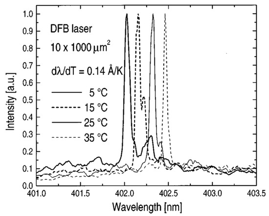
Figure 1.
Emission spectra of an InGaN/GaN-based, electrically injected, pulsed DFB laser at a constant injection current of 1.1 × Ith, a threshold current density of Jth = 16 kA/cm2, and at four different device temperatures of 5 °C, 15 °C, 25 °C, and 35 °C. Under these conditions, a temperature tuning coefficient of dλ/dT = 0.14 Å/K was observed. The presented Figure 1 is a re-publication of the 4th figure in reference [6].
The tuning rate of dλ/dT = 0.14 Å/K measured in this electrically pumped device will—within a small tolerance—also be observed in the presented optically pumped DFB laser. The tiny allowed deviation is a clear indication for the necessity to have a reliable means for a precise mutual alignment of the grating period and the gain peak. Once the correct grating period Λ will be known, it can be holographically exposed and developed using a thin photoresist layer, dry-etched across the thin p-cladding and deeply into the top waveguide. After grating mask removal, epitaxial over-growth involving the entire upper Al0.08Ga0.92N cladding and the GaN-based top contact can be performed. Adopting such a two-step fabrication strategy guarantees the correct grating period in an efficient way.
Based on a similar experiment with an optically pumped ZnO-based DFB laser [23], it became clear that searching for the ideal wavelength match between the active region’s gain peak and the grating’s Bragg resonance is indeed not a trivial task at all. On the contrary, it typically requires several feedback loops with processing, epitaxial over-growth, and characterization. Identifying already beforehand the correct grating parameters will thus result in considerable savings of time and processing effort.
Concerning the optical confinement factor in the QW region, we refer to [24], where this quantity has already been calculated. In Figure 2, we obtained, with a 500 nm thick upper cladding layer, roughly 3.8% total overlap between optical mode and QWs. However, when the upper cladding layer thickness is reduced to about 100 nm, the overlap of the QWs increases—at the ‘cost’ of much smaller side maxima in the 4 µm thick GaN layer—to a maximum value of 5.0%. This is shown in Figure 2 below.
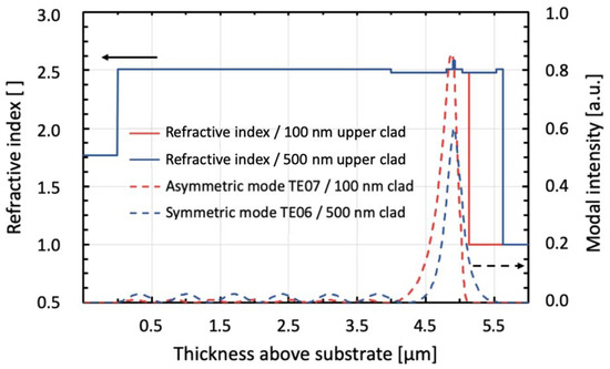
Figure 2.
Comparison of optical waveguide profile and simulation using either a standard thickness (500 nm, blue line) or a very thin (100 nm, red line) upper cladding layer. The refractive index profile is drawn on the left; modal intensity on the right y-axis.
Because of the much smaller side maxima in the 4 µm thick GaN layer, the modal intensity—and thus the optical confinement factor of the InGaN-based MQWs in the asymmetric configuration —gets roughly 35% larger than the one of the symmetric device. The solid red line corresponds to the 100 nm thick upper cladding being at the origin of the increased optical confinement factor.
3. Design Considerations
For this reason, we propose in the present article the use of a non-destructive measurement technique to allow a perfect match between the material’s gain peak and the Bragg resonance of the DFB laser’s diffraction grating. By carefully adjusting this fundamental parameter, not only an ideal alignment between these two key features of DFB lasers will be assured, but it will also become clear how much maximal output power and single-mode tuning range can be expected in a completed device. In order to profit from a ‘good optical interaction’ between the optical pump source and the MQW active region of this DFB laser, epitaxial growth needs to be interrupted after the first 100 nm of the top cladding layer. This way, it is guaranteed that only a small portion of the vertically incoming UV radiation will be absorbed already in the top cladding. Similar as in the work of Shank et al. [21], interferometric optical pumping will then be used for this experiment. It serves essentially two different purposes: Just like in classical optical pumping, it will bring the InGaN/GaN-based MQW region and thus the laser resonator above threshold [23]. But, in contrast to a ‘normal’ Fabry—Pérot laser device, the laterally focalized input radiation will—before re-emitting λ = 400 nm light from the MQW region—illuminate the sample surface not only as an ordinary pump beam, but rather in the form of a narrow, laterally focalized two-beam interference pattern. This pattern consists of interference fringes, which must—as calculated for instance in Born and Wolf [25]—have a very short period of Λm:
In our case, λ = 400 nm corresponds to the emission wavelength of the In0.15Ga0.85N MQWs, m = 3 is the diffraction order, and neff = 2.5 is the effective refractive index of the InGaN/GaN waveguide. When using this set of parameters—corresponding to a gain-coupled third-order (m = 3) DFB grating designed for an emission wavelength in the violet–blue 400 nm spectral range—this results in a required grating period of Λm = 240 nm. In order to obtain the angle between the surface normal and one of the interfering input beams, we have to solve the complete grating formula (Equation (2)) for the input angle θin below [26,27,28]. It is important to use for the grating exposure the UV radiation of a frequency-tripled Nd:YAG laser at an input wavelength of λin = 354.67 nm:
Assuming a symmetric geometry, one can then calculate the required angle between the interfering UV input beams. According to Equation (2), an optical exposure at a wavelength of λ = 354.67 nm and under symmetric angles of = ±47.637° vis-à-vis the surface normal will produce the desired interference pattern having the previously calculated period of Λ = 240 nm. The experimental configuration of this interferometric optical pumping is schematically shown in Figure 3 below.
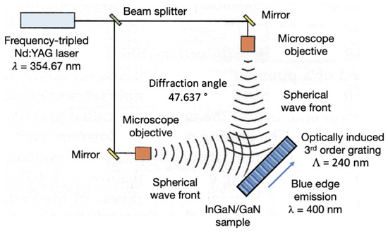
Figure 3.
Schematic view of the experimental setup of an interferometric UV-radiation-induced, optically pumped DFB laser. Optical emission at λ = 400 nm takes place from the InGaN/GaN sample schematically shown in the lower right corner.
For the radiation emitted at λ = 400 nm from the In0.15Ga0.85N/GaN MQW region, we will have to use Equation (3). With diffraction orders/indices of m = 3, ℓ = 0, or ℓ = 3, we will obtain two opposing, equally large DFB modes at angles of θm=3,ℓ=0,3 = ±90°. These waves are thus both traveling parallel to the sample surface, and they will therefore not suffer any refraction when leaving the InGaN/GaN waveguide. However, there are two additional radiation modes. Their indices are given by m = 3, ℓ = 1, or by m = 3 and ℓ = 2. The corresponding angles of θm=3,ℓ=1,2 = ±19.471° are smaller than the critical angle of total internal reflection (θc = arc sin(1/nInGaN/GaN) = 23.578°). Therefore, these two modes will be able to radiate and thus become visible from outside of the InGaN/GaN crystal [29,30].
4. Predicted Results
Depending on the grating tooth shape (i.e., the relative amplitude of its different Fourier components), a larger fraction of the radiation will be emitted into the 0th and 3rd order modes. Therefore, the light emission in the directions parallel to the crystal’s surface will become the dominant one. As mentioned in the previous section, the light from the 1st and the 2nd order radiation modes will be weaker and essentially serve the purpose of monitoring the produced DFB laser emission.
Table 1 shows, in form of a summary, the most important parameters of the optical absorption/re-emission processes, along with the relevant wavelengths, diffraction orders, and diffraction angles.

Table 1.
Type of process, corresponding wavelength, grating period, diffraction order/index, diffraction angle, and general remarks occurring in interferometric optical pumping of an InGaN/GaN-based DFB laser.
While in the direction parallel to the length of the illuminated stripe, the period of the interference pattern needs obviously to be preserved (and kept in resonance with the grating period), the light in the perpendicular direction is being focalized down to a width of <10 µm. Together, this constitutes a sufficiently elevated intensity level—namely I ≥ 5 kW/(10 µm × 2 mm) = 25 MW/cm2—to result in the generation of an optically pumped In0.15Ga0.85N/GaN-based DFB laser. As a comparison, we observed in reference [5] a threshold intensity of 6.25 MW/cm2 for an optically pumped, index-coupled InGaN/GaN-based DFB laser.
When illuminating the laser surface—like in a two-beam interference pattern—with a sinusoidally modulated intensity, one can in first approximation assume that carrier diffusion will be isotropic in all spatial directions. As a result of this, the grating will become somewhat ‘washed out’ and therefore show a considerably reduced coupling constant κ. To take this effect into account, κ is lowered to about 50% of its theoretically possible ideal value. In practice, this means that in order to maintain the κL product at a reasonably elevated level (κL = 1), a twice as long laser stripe will have to be pumped.
Since the different wavelengths and diffraction orders are quite subtle to understand, we show in Figure 4 a schematic view of the sample along with the different relevant beams, their wavelengths, and their corresponding diffraction orders/angles. As already shown both in Figure 3 and in Table 1, holographic grating exposure will take place at λ = 354.67 nm under angles of θm,ℓ = ±47.637°.
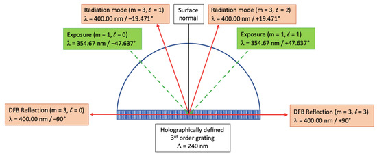
Figure 4.
Schematic view of the different illuminating and emitted beams of interferometric UV exposure (m = 1, ℓ = 0, 1) generating an optically pumped violet–blue DFB laser. The emitted radiation modes (m = 3, ℓ = 1, 2) will not be totally reflected and therefore be visible from the outside. The emissions at θm,ℓ = ±90° (m = 3, ℓ = 0, 3), however, are leaving the material at the two opposing, perpendicular end facets of the crystal and will therefore not undergo any directional change.
In order to illustrate the proposed functioning of the resulting single-mode semiconductor laser, we show in Figure 5 a series of simulated, normalized emission spectra (output power vs. emission wavelength) at five representative interference angles between two extreme values of = 47.732° and = 47.543°. They still allow a sufficiently high gain margin for the lasing DFB mode. A theoretical gain peak for three typical device temperatures as well as a (constant) threshold gain (red) are shown as dashed lines. As a considerable advantage compared to index-coupled DFB lasers, the presented optical pumping scheme allows tuning of the emission wavelength by simply changing the angle between the two interfering UV input laser beams. Fine tuning of the emission wavelength can be achieved by changing the DFB laser’s refractive index via the device temperature.

Figure 5.
Optical output power (left y-axis) as a function of emission wavelength (x-axis) at five different interference angles, gain peak at three different device temperatures, and constant threshold gain (right y-axis) of an optically pumped interferometric DFB laser. Tuning of the DFB laser was accomplished by changing the interferometric angle between the two input beams from 47.732° (399.4 nm) to 47.543° (400.6 nm).
For an easier understanding of the different wavelength-dependent features of this device, we present in Figure 6 a curve displaying DFB emission wavelength as a function of the interference angle.
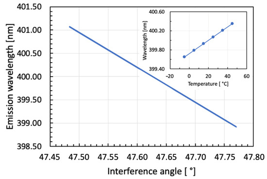
Figure 6.
DFB laser emission wavelength as a function of the interference angle. The inset shows—as a comparison—the wavelength tuning of a classical DFB laser as a function of temperature.
As shown in Figure 6, the DFB laser wavelength can be tuned in a wide range by directly changing the grating period (blue curve without dots). This is accomplished via changing the diffraction angle of the UV-laser-induced interference pattern. The corresponding angular values—as measured between surface normal and one interferometer arm only—measure between 47.732° (399.4 nm) and 47.543° (400.6 nm). The inset of Figure 6 shows emission wavelength as a function of device temperature in steps of 10 K between −5 °C and 45 °C. This tuning is due to the temperature-induced effective refractive index change in the In0.15Ga0.85N/GaN active region; namely, dλ/dT = 0.14 Å/K.
By using this interferometric method, the shape, and the two different tuning rates of gain and DFB peak in Figure 5, the maximal single-mode tuning range of this device can be estimated [15]. Obviously, the different tuning rates of lasing and gain peak (dλDFB/dT ≈ 0.14 Å/K; dλgap/dT ≈ 0.42 Å/K)—as well as the net gain margin vis-à-vis the threshold gain—limit this maximal tuning range. Altogether, a limit of ΔTmax = 80 K is found. Accordingly, we present in Figure 7 the corresponding L−I curves for five typical device temperatures between −40 °C and +40 °C (in steps of 20 K). The output power in this figure corresponds to roughly 10% of the experimentally observed pulsed power levels in reference [6].
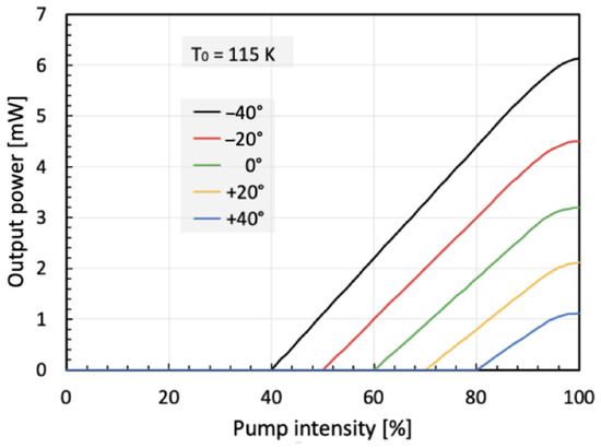
Figure 7.
Optical output power vs. optical pump intensity of a UV-pumped interferometric DFB laser for different device temperatures between −40 °C and +40 °C. A maximum single-mode power level of 6 mW at −40 °C is observed. The 100% value of the pump intensity corresponds to a value on the order of 25 MW/cm2.
By using a pulsed and collimated, frequency-tripled Nd:YAG laser (Ppulse = 5 kW, λNd:YAG = 354.67 nm), a 3rd-order diffraction grating with a period of 240 nm can be holographically and transiently defined on the surface of the presented InGaN/GaN MQW sample. Upon further increasing the optical pump power, a gain-coupled DFB laser in the λ = 400 nm spectral region will be generated. For this purpose, two-beam interference with a lateral focalization employing a cylindrical lens is utilized. The choice of this particular laser type and emission wavelength is actually based on the following reasoning: The laser must emit radiation with a photon energy being situated in between the bandgap energy of GaN in the top waveguide layer (EgGaN = 3.39 eV, λedge = 365 nm) and of 8% AlGaN in the top cladding layer (EgAlGaN = 3.55 eV, λedge = 350 nm). As shown in this paper, a frequency-tripled, pulsed high-power Nd:YAG laser with an emission wavelength of 354.67 nm is indeed exactly at the required wavelength. In the somewhat smaller bandgaps of the 15% InGaN-based QWs and the GaN-based waveguide layers, its radiation will be heavily absorbed, while in the slightly larger bandgap of the 8% AlGaN-based upper cladding layer, there will be almost no absorption at all. With the small thickness of this layer, optical absorption will be almost totally suppressed.
5. Possible Applications
Based on the idea presented in this paper, both fabrication and the most important characterization features of a broadly tunable InGaN/GaN-based DFB laser have been described. An all-optical technique to mutually align gain peak and Bragg resonance of a short-wavelength DFB laser constitutes—prior to rather dry etching of its third-order diffraction grating—an ideal means to maximize its performance. It goes without explicitly saying that the preliminary testing suggested here can be performed in the absence of a sophisticated grating fabrication or epitaxial over-growth of this laser structure. This will result in a faster feedback loop to the crystal growers and finally a more efficient fabrication procedure. In addition, such a device optimization will positively influence output power as well as tuning behavior or optical linewidth of these lasers. Used as surface-emitting DFB lasers, for instance, by defining 2nd- instead of 3rd-order diffraction gratings, such devices will also be very well suited as important building blocks of more complex photonic integrated circuits. Mainly due to their special geometry—which is in fact closely linked to their emission characteristics—such devices carry the potential to work without optical laser mirror fabrication. In particular, this means that the fabrication of the proposed DFB lasers does not necessarily require any advanced semiconductor mirror etching, facet cleaving, or electrical contact evaporation steps. Since InGaN, GaN, and AlGaN semiconductors are mechanically extremely robust, chemically highly inert, and very radiation-hard materials, their use as DFB laser sources will potentially open various entirely new paths and opportunities for different high-end applications.
Of particular interest in this context are applications related to high-resolution document scanning and laser printing. When employing for this purpose InGaN/GaN-based violet–blue semiconductor lasers or laser arrays, it is possible to handle documents with a high-resolution of 1200 dots per inch (dpi)—resulting in an ultimately small linear pixel or focal spot dimension of 25.4 mm/1200 = 21.17 µm. In order to produce focal spots as small as 21.17 µm, it is necessary to work with laser light sources and focalizing optics components being very close to their diffraction limit. Only high-performing single-mode devices can actually be focalized to result in such sufficiently small spot sizes.
More recently, GaN-based DFB lasers have as well become interesting for applications in free-space communications, underwater technology, atomic clocks, and LiDAR sensing [31,32].
6. Conclusions
In the proposed experimental setup, fabrication, and measurement technology, a widely tunable InGaN/GaN-based DFB laser has been described. Its wavelength tuning will be accomplished via a change in either the device temperature or the interference angle of its doubled optical pump beams. The proposed method makes it possible to non-invasively assess the correct interference angle in order to continue afterwards with etching the desired grating period, performing the epitaxial over-growth, and processing the structure into an electrically injected DFB laser. In future experiments, careful adjustments—both in crystal quality and in device design—carry the intrinsic potential to lead to a marked performance improvement. Thanks to optimized crystal growth conditions, more advanced fabrication processes and a higher level of processing technology—along with better characterization tools—measurement results with an increased quality and most notably a higher degree of stability are expected.
In future experiments, the information collected from the technique suggested in this article might be used as follows. Growth will be interrupted already after the top waveguide layer. As a next step, interferometric optical pumping will be carried out. As soon as the most suitable DFB grating period is known, holographically exposed, and fabricated by dry etching, the sample will go back to the growth chamber, in which the top cladding and the top contact will be deposited.
7. Patents
No specific patent issues related to the work suggested in this article need to be discussed at this place.
Author Contributions
Conceptualization, D.H.; methodology, D.H.; software, D.H.; validation, D.H., H.B. and D.P.B.; formal analysis, H.B.; investigation, D.H.; resources, D.P.B.; data curation, H.B.; writing—original draft preparation, D.H.; writing—review and editing, D.H.; visualization, D.H.; supervision, H.B.; project administration, D.P.B.; funding acquisition, D.H. All authors have read and agreed to the published version of the manuscript.
Funding
This research received no external funding.
Data Availability Statement
The data presented in this study are available on request from the corresponding author. The data are not publicly available due to privacy reasons.
Acknowledgments
The authors would like to thank the former Institute of Physics at the University of Neuchâtel for making available all necessary cleanroom and characterization equipment, express gratitude for the generous support provided by the Professorship Program of the Swiss National Science Foundation, and acknowledge all valuable discussions with and encouragements by John E Epler at Lumileds, Inc., San Jose, CA, USA, Gary Evans at the Southern Methodist University in Salt Lake City, UT, USA, and Dan Botez at the University of Wisconsin in Madison, NY, USA.
Conflicts of Interest
The authors declare no conflict of interest.
References
- Kogelnik, H.; Shank, C.V. Stimulated emission in a periodic structure. Appl. Phys. Lett. 1971, 18, 152–154. [Google Scholar] [CrossRef]
- Borchert, B.; Gessner, R.; Stegmüller, B. Advanced 1.55 µm Quantum-Well GaInAlAs laser diodes. Jpn. J. Appl. Phys. 1994, 33, 1034–1039. [Google Scholar] [CrossRef]
- Nishimura, K.; Asakura, H.; Yamauchi, S.; Suzuki, T.; Nakai, Y.; Yamaguchi, Y.; Kageyama, T.; Mitaki, M.; Endo, Y.; Naoe, K. 225-Gb/s PAM4 Operation using Lumped-Electrode-Type EA-DFB Laser for 5- and 10-km Transmission with Low TDECQ. In Optical Fiber Communication (OFC); Technical Digest Series; Optica Publishing Group: Washington, DC, USA, 2023. [Google Scholar]
- Nakamura, S.; Senoh, S.; Nagahama, S.-I.; Iwasa, N.; Yamada, T.; Matsushita, T.; Kiyoku, H.; Sugimoto, Y. InGaN-based multi-quantum-well-structure laser diodes. Jap. J. Appl. Phys. 1996, 35, L74–L76. [Google Scholar] [CrossRef]
- Hofstetter, D.; Thornton, R.L.; Kneissl, M.; Bour, D.P.; Dunnrowicz, C. Demonstration of an InGaN/GaN-based optically pumped multiquantum well distributed-feedback laser using holographically defined third-order gratings. Appl. Phys. Lett. 1998, 73, 1928–1930. [Google Scholar] [CrossRef]
- Hofstetter, D.; Thornton, R.L.; Romano, L.T.; Bour, D.P.; Kneissl, M.; Donaldson, R.M. Room-temperature pulsed operation of an electrically injected InGaN/GaN multi quantum well distributed feedback lasers. Appl. Phys. Lett. 1998, 73, 2158–2160. [Google Scholar] [CrossRef]
- Slight, T.J.; Odedina, O.; Meredith, W.; Docherty, K.E.; Kelly, A.E. InGaN/GaN distributed feedback laser diodes with deeply etched sidewall gratings. IEEE Photonics Technol. Lett. 2016, 28, 2886–2888. [Google Scholar] [CrossRef]
- Kang, J.H.; Martens, M.; Wenzel, H.; Hoffmann, V.; John, W.; Einfeldt, S.; Wernicke, T.; Kneissl, M. Optically pumped DFB lasers based on GaN using 10th-order laterally coupled surface gratings. IEEE Photonics Technol. Lett. 2017, 29, 138–141. [Google Scholar] [CrossRef]
- Slight, T.J.; Watson, S.; Viola, S.; Yadav, A.; Stańczyk, S.; Grzanka, S.; Gwyn, S.; Rafailov, E.U.; Perlin, P.; Najda, S.P.; et al. Recent progress in distributed feedback InGaN/GaN laser diodes. In Proceedings of the SPIE Photonics West OPTO 2019 Proceedings, Novel In-Plane Semiconductor Lasers XVIII, San Francisco, CA, USA, 1 March 2019; Volume 10939, pp. 51–56. [Google Scholar] [CrossRef]
- Holguin-Lerma, J.A.; Kong, M.; Alkhazragi, O.; Sun, X.B.; Ng, T.K.; Ooi, B.S. 480-nm- distributed feedback InGaN laser diode for 10.5-Gbit/s visible-light communication. Opt. Lett. 2020, 45, 742–745. [Google Scholar] [CrossRef]
- Najda, S.P.; Perlin, P.; Suski, T.; Marona, L.; Leszczyńsky, M.; Wisniewski, P.; Stańczyk, S.; Schiavon, D.; Slight, T.; Watson, M.A.; et al. GaN Laser Diode Technology for Visible-Light Communications. Electronics 2022, 11, 1430. [Google Scholar] [CrossRef]
- Emoto, K.; Koizumi, T.; Hirose, M.; Jutori, M.; Inoue, T.; Ishizaki, K.; De Zoysa, M.; Togawa, H.; Noda, S. Wide-bandgap GaN-based watt-class photonic-crystal lasers. Commun. Mater. 2022, 3, 72. [Google Scholar] [CrossRef]
- Xu, Z.Y.; Niu, W.Q.; Liu, Y.; Lin, X.H.; Cai, J.F.; Shi, J.; Wang, X.; Wang, G.; Zhang, Z.; Jiang, F.; et al. 31.38 Gb/s GaN-based LED array visible light communication system enhanced with V-pit and sidewall quantum well structure. Opto-Electron. Sci. 2023, 2, 230005. [Google Scholar] [CrossRef]
- Pankove, J.I.; Miller, E.A.; Richman, D.; Berkeyheiser, J.E. Electroluminescence in GaN. J. Lumin. 1971, 4, 63–66. [Google Scholar] [CrossRef]
- Nakamura, S.; Senoh, M.; Nagahama, S.-I.; Iwasa, N.; Matsushita, T.; Mukai, T. Blue InGaN-based laser diodes with an emission wavelength of 450 nm. Appl. Phys. Lett. 2000, 76, 22–24. [Google Scholar] [CrossRef]
- Khoury, M.; Li, H.; Li, P.; Chow, Y.C.; Bonef, B.; Zhang, H.; Wong, M.S.; Pinna, S.; Song, J.; Choi, J.; et al. Polarized monolithic white semipolar (20-21) InGaN light-emitting diodes grown on high quality (20-21) GaN/sapphire templates and its applications to visible light communication. Nano Energy 2020, 67, 104236. [Google Scholar] [CrossRef]
- Nakamura, S.; Krames, M.R. History of gallium-nitride-based light-emitting diodes for illumination. Proc. IEEE 2013, 101, 2211–2220. [Google Scholar] [CrossRef]
- Pathak, C.S.; Dadwal, U. Recent Advancements in GaN LED Technology. In Light-Emitting Diodes: New Perspectives; Tabbakh, T.A., Anandan, D., Sheldon, M.J., Tyagi, P., Alfaifi, A., Eds.; IntechOpen: London, UK, 2022. [Google Scholar] [CrossRef]
- Kostic, A.M.; Kremic, M.M.; Djokic, L.S.; Kostic, M.B. Light-emitting diodes in street and and roadway lighting-a case study involving mesopic effects. Light. Res. Technol. 2013, 45, 217. [Google Scholar] [CrossRef]
- DenBaars, S.P.; Feezell, D.; Kelchner, K.; Pimputkar, S.; Pan, C.-C.; Yen, C.-C.; Tanaka, S.; Zhao, Y.; Pfaff, N.; Farrell, R.; et al. Development of gallium-nitride-based light-emitting diodes (LEDs) and laser diodes for energy-efficient lighting and displays. Acta Mater. 2013, 61, 945–951. [Google Scholar] [CrossRef]
- Shank, C.V.; Bjorkholm, J.E.; Kogelnik, H. Tunable distributed-feedback dye laser. Appl. Phys. Lett. 1971, 18, 395–396. [Google Scholar] [CrossRef]
- Zory, P. Laser oscillation in leaky corrugated optical waveguides. Appl. Phys. Lett. 1973, 22, 125–128. [Google Scholar] [CrossRef]
- Hofstetter, D.; Bonetti, Y.; Giorgetta, F.R.; El-Shaer, A.-H.; Bakin, A.; Waag, A.; Schmidt-Grund, R.; Schubert, M.; Grundmann, M. Demonstration of an ultraviolet ZnO-based optically pumped third order distributed feedback laser. Appl. Phys. Lett. 2007, 91, 111108. [Google Scholar] [CrossRef]
- Hofstetter, D.; Bour, D.P.; Thornton, R.L.; Johnson, N.M. Excitation of a higher order transverse mode in an optically pumped In0.15Ga0.85N/In0.05Ga0.95N-based multiquantum well laser structure. Appl. Phys. Lett. 1997, 70, 650–652. [Google Scholar] [CrossRef][Green Version]
- Born, M.; Wolf, E. Principles of Optics, 7th ed.; section 7.6 on ‘Multiple-beam Interference’, formula (14); Cambridge University Press: Cambridge, UK, 1999; pp. 326–327. [Google Scholar] [CrossRef]
- Kogelnik, H.; Shank, C.V. Coupled-wave theory of distributed feedback lasers. J. Appl. Phys. 1973, 25, 2327–2335. [Google Scholar] [CrossRef]
- Scifres, D.R.; Burnham, R.D.; Streifer, W. Distributed-feedback single heterojunction GaAs diode laser. Appl. Phys. Lett. 1974, 25, 203–206. [Google Scholar] [CrossRef]
- Burnham, R.D.; Scifres, D.R.; Streifer, W. Single-heterostructure distributed-feedback GaAs-diode lasers. IEEE J. Quantum Electron. 1975, 11, 439–449. [Google Scholar] [CrossRef]
- Liu, M.; Liu, Y.; Zhang, G.; Peng, Z.; Li, D.; Ma, J.; Xuan, L. Organic holographic polymer dispersed liquid crystal distributed feedback laser from different diffraction orders. J. Phys. D Appl. Phys. 2016, 49, 465102. [Google Scholar] [CrossRef]
- Zhou, P.; Niu, L.; Hayat, A.; Cao, F.; Zhai, T.; Zhang, X. Operating characteristics of high-order distributed feedback polymer lasers. Polymers 2019, 11, 258. [Google Scholar] [CrossRef]
- Johnson, L.; Mahoney, M.; Bevilacqua, E.; Stehman, S.; Domke, G.; Beier, C. Fine-resolution landscape-scale biomass mapping using a spatiotemporal patchworl of LiDAR coverages. Int. J. Appl. Earth Obs. Geoinf. 2022, 114, 103059. [Google Scholar] [CrossRef]
- Ramsey, N.F. History of early atomic clocks. Metrologia 2014, 42, S1–S3. [Google Scholar] [CrossRef]


Disclaimer/Publisher’s Note: The statements, opinions and data contained in all publications are solely those of the individual author(s) and contributor(s) and not of MDPI and/or the editor(s). MDPI and/or the editor(s) disclaim responsibility for any injury to people or property resulting from any ideas, methods, instructions or products referred to in the content. |
© 2023 by the authors. Licensee MDPI, Basel, Switzerland. This article is an open access article distributed under the terms and conditions of the Creative Commons Attribution (CC BY) license (https://creativecommons.org/licenses/by/4.0/).