Abstract
The direct growth of ferroelectric films onto flexible substrates has garnered significant interest in the advancement of portable and wearable electronic devices. However, the search for an optimized bottom electrode that can provide a large and stable remnant polarization is still ongoing. In this study, we report the optimization of an oxide-based LaNiO3 (LNO) electrode for high-quality Pb(Zr0.52Ti0.48)O3 (PZT) thick films. The surface morphology and electrical conductivity of sol-gel-grown LNO films on a fluorophlogopite mica (F-mica) substrate were optimized at a crystallization temperature of 800 °C and a film thickness of 120 nm. Our approach represents the promising potential pairing between PZT and LNO electrodes. While LNO-coated F-mica maintains stable electrical conductivity during 1.0%-strain and 104-bending cycles, the upper PZT films exhibit a nearly square-like polarization–electric field behavior under those stress conditions. After 104 cycles at 0.5% strain, the remnant polarization shows decreases as small as ~14%. Under flat (bent) conditions, the value decreases to just 81% (49%) after 1010 fatigue cycles and to 96% (85%) after 105 s of a retention test, respectively.
1. Introduction
Ferroelectric oxide films have played an important role in modern electronic devices due to their inherently large dielectric, piezoelectric, and pyroelectric coefficients compared to other materials [1,2,3]. These superior properties have been applied in dielectric gates for field effect transistors [4], microelectronic mechanical systems for robots [5], energy harvesting systems from wasted mechanical vibrations [6], and non-volatile random access memory applications [7]. Instead of conventional solid-state electronics, flexible film-based electronic devices are currently in high demand, such as portable personal electronics and skin-attachable health monitoring sensors [8,9,10]. To meet such demands, there have been many efforts to fabricate flexible ferroelectric films with high crystalline quality.
Until now, there have been two representative approaches to obtain flexible ferroelectric oxide films. One is the direct growth method, which uses flexible substrates with high melting temperatures [11,12,13]. The other is the transfer method, in which films are deposited onto soluble substrates or buffer layers and then removed to obtain free-standing films. Such free-standing films are transferred onto polymer substrates to endow the film with flexibility [14,15,16]. Of the two methods, the direct growth on flexible substrates has frequently been adopted due to the advantages of its one-step growth capability and large-scale processing [17]. For example, Kingon et al. used a copper (Cu) foil substrate for sol-gel-grown Pb(Zr,Ti)O3 (PZT) films with flexible functionality [18]. They annealed the film at a high temperature of 650 °C and an extremely low oxygen partial pressure of 10−16 atm to enhance the crystallinity of the PZT without oxidizing the Cu substrate. The PZT film deposited on the Cu foil showed normal ferroelectric switching behavior with a remnant polarization of 20 μC/cm2. Jiang et al. used a mica substrate for pulsed laser-deposited PZT films with flexible functionality [19]. They employed a SrRuO3 bottom electrode and a CoFe2O4 buffer layer to reduce the lattice mismatch between the film and the substrate. The PZT film deposited on SrRuO3-coated mica substrate showed a remnant polarization of 60 μC/cm2 and the robust operation of non-volatile memory devices in the bent state. While the above two reports are innovative, an optimized electrode with facile fabrication and high conductivity is required for the application of ferroelectric film-based flexible electronic devices.
The perovskite structure (ABO3), with its distinctive arrangement of A and B cations and oxygen anions, is crucial in materials science. PZT, a notable perovskite, is valued for its piezoelectric properties, and used in sensors and actuators. Perovskite structures play a vital role in advancing technology, spanning catalysis and electrochemistry [20,21,22]. Meanwhile, LaNiO3 (LNO) has a perovskite structure and a low resistance. In addition, it is easy to manufacture in a solution and has a relatively tailorable lattice mismatch margin with PZT [23]. Sol-gel deposition has the advantage of enabling large-area deposition and a slightly lower importance of lattice mismatch compared to other deposition methods. Therefore, we have selected LNO with sol-gel deposition as the candidate material for the electrode optimized for PZT.
In this paper, we used a LNO bottom electrode for the sol-gel-grown PZT films with flexible functionality. On top of a flexible fluorophlogopite mica (F-mica) substrate, the LNO bottom electrode and PZT ferroelectric films were sequentially grown using a conventional spin-coating method. The crystallization temperature and thickness were found to strongly influence the physical properties of LNO and were optimized at 800 °C and 120 nm, respectively. A smooth surface with a root mean square roughness of Rrms = 1.7 nm and an electrical resistivity of ρ = 3.3 × 10⁻³ Ω cm (electrical conductivity of σ = 303 Ω−1 cm−1) was achieved for the optimized LNO film without losing its bendability at up to 1.0% of strain and 104 repetitions of bending cycles. The optimized LNO bottom electrode results in a high remnant polarization of 57.1 μC/cm2, high dielectric constant of 746 at 1 kHz, and a low dielectric loss of 0.067 at 1 kHz for flexible PZT films. The 1010 cycle fatigue and 105 s retention tests demonstrate the relatively good ferroelectric random access memory characteristics in flat and bent PZT films grown on optimized LNO-coated F-mica substrates.
2. Experimental Details
2.1. Reagents
The LNO solution was prepared using lanthanum(III) nitrate hexahydrate (La(NO3)3·6H2O) and nickel(II) acetate tetrahydrate (Ni(CH3CO2)2·4H2O) precursors (purity > 99.99%, Sigma Aldrich, Burlington, MA, USA). As schematically shown in Figure S1, nickel(II) acetate tetrahydrate was mixed with acetic acid (CH3COOH) solvent (purity > 99.5%, Sigma Aldrich, Burlington, MA, USA) and stirred at room temperature for 30 min. An equal molar amount of lanthanum(III) nitrate hexahydrate was then added, followed by mixing and stirring at room temperature for 30 min. During the stirring, deionized water (H2O) and formamide (CH3NO) (purity > 99.5%, SAMCHUN, Seoul, Republic of Korea) were added to achieve a 0.1 M concentration of the solution and to prevent cracking during annealing, respectively. Finally, the solution was filtered to enhance its purity. PZT (Zr:Ti = 52:48) solution was commercially prepared. (Quintess Co., Ltd., Incheon, Republic of Korea).
The LNO solution was prepared using lanthanum(III) nitrate hexahydrate (La(NO3)3·6H2O) and nickel(II) acetate tetrahydrate (Ni(CH3CO2)2·4H2O) precursors (purity > 99.99%, Sigma Aldrich, Burlington, MA, USA). As schematically shown in Figure S1, nickel(II) acetate tetrahydrate was mixed with acetic acid (CH3COOH) solvent (purity > 99.5%, Sigma Aldrich, Burlington, MA, USA) and stirred at room temperature for 30 min. An equal molar amount of lanthanum(III) nitrate hexahydrate was then added, followed by mixing and stirring at room temperature for 30 min. During the stirring, deionized water (H2O) and formamide (CH3NO) (purity > 99.5%, SAMCHUN, Seoul, Republic of Korea) were added to achieve a 0.1 M concentration of the solution and to prevent cracking during annealing, respectively. Finally, the solution was filtered to enhance its purity. PZT (Zr:Ti = 52:48) solution was commercially prepared. (Quintess Co., Ltd., Incheon, Republic of Korea).
2.2. Film Fabrication
The LNO solution was spin-coated onto a F-mica [KMg3(AlSi3O10)F2] (MTI, Richmond, CA, USA) substrate at 3000 rpm for 30 s. The film was then dried at 300 °C for 5 min to remove the solvent, annealed at 400 °C for 5 min to remove residual organic impurities, and finally crystallized at 600~900 °C for 3 min. Note that the drying and annealing temperatures were determined based on the results of thermogravimetric analysis (STA4098PC, NETZSCH, Selb, Germany) and differential scanning calorimetry (404F1, NETZSCH, Selb, Germany) results (Figure 1a,b). The sequential side view SEM revealed that 20 nm thick LNO can be formed on the surface with a single coating process. Spin-coating and crystallization were iterated to achieve the desired thickness of LNO. On the LNO-coated F-mica substrate, a commercial PZT (Zr:Ti = 52:48) solution was spin-coated at 4000 rpm for 30 s and pyrolyzed on a hot plate at 450 °C for 7 min to remove the solvent and organic residues. Additional PZT solution was spin-coated and pyrolyzed under the same conditions. Two layers of pyrolyzed PZT were crystallized in a box furnace (AJ-RTA, Ajeon Co., Namyangju, Republic of Korea) at 650 °C for 30 min. Finally, the F-mica substrate was stripped to a thickness of 10 μm using Kapton tape.
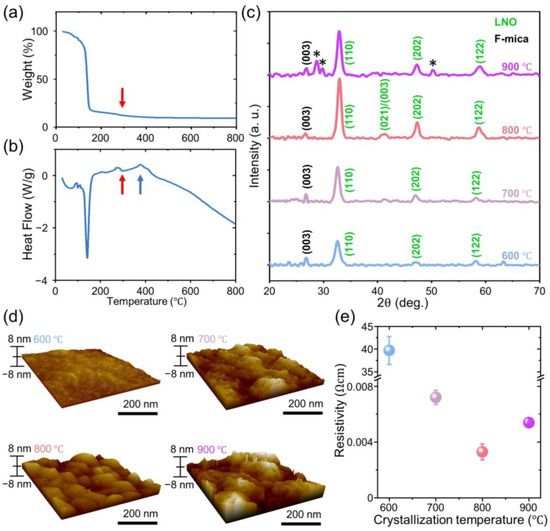
Figure 1.
(a) Thermogravimetric analysis and (b) differential scanning calorimetry results of LaNiO3 (LNO) solution. The solution undergoes drying at ~285 °C and crystallization at ~377 °C, showing a step-down and a bulb in the heat flow of (b), respectively. The red (and blue) arrow is used to indicate the drying (crystallization) temperature in (a,b), respectively. Crystallization temperature-dependent (c) X-ray diffraction pattern, (d) surface morphology, and (e) electrical resistivity at room temperature of LNO films on F-mica substrate. In (c), the impurity peaks of La(OH)3 are marked with asterisks.
2.3. Characterization
The crystalline structure of the films was characterized via high resolution X-ray diffraction (XRD) using Cu-Kα radiation (X’Pert Powder Diffractometer, PANalytical, Malvern, UK). Surface and cross-sectional morphologies were examined via atomic force microscopy (NX10, PSIA, Suwon, Republic of Korea) and field emission scanning electron microscopy (S-4300SE, HITACHI), respectively. The temperature-dependent resistivity of the LNO films was measured using a physical property measurement system (PPMS-9, Quantum Design, San Diego, CA, USA). For the resistivity measurements, a silver conductive epoxy (Electron Microscopy Sciences, Radnor, PA, USA) was attached to the film and subsequently cured at 120 °C using a hot plate for 1 h (DAIHAN Scientific, Wonju, Republic of Korea). A high-purity (>99.995%) 0.002 inch-diameter gold wire (Alfa Aesar, Ward Hill, MA, USA) was used for accurate resistivity measurements. The resistivity measurement was conducted on three different films grown under the same conditions to ensure statistical relevance. The ferroelectric hysteresis loop and complex dielectric constant were obtained for PZT films using a ferroelectric tester (Precision Multiferroic Tester, Radiant Technologies, Inc., Albuquerque, NM, USA) and an LCR meter (4284A, Hewlett-Packard, Palo Alto, CA, USA), respectively. For the ferroelectric and dielectric measurements, a 0.03 mm2 Pt top electrode was sputter deposited using a coater (Sputter coater 108, Cressington, Watford, UK).
3. Results and Discussion
Figure 1a,b show the film manufacturing conditions of the LNO solution. Figure 1a presents the thermogravimetric analysis, indicating a sharp decrease at 136 °C and a mild decrease at 285 °C, above which the LNO solution can be dried, removing its solvent. Furthermore, Figure 1b presents the result of the differential scanning calorimetry, where crystallization, as well as the previously mentioned drying effect, were simultaneously observable. From 377 °C, the heat flow tends to decrease as a negative number. Therefore, the LNO solution was crystallized at subsequent temperatures of 600 °C, 700 °C, 800 °C, and 900 °C.
Figure 1c shows the high-resolution X-ray diffraction pattern of LNO films on an F-mica substrate. To clarify the diffraction peaks of LNO, the film is slightly tilted (~1°). All diffraction peaks can be well indexed using the Miller indices of LNO (green) and F-mica (black) without any secondary peaks. As the temperature increases, the crystallinity of LNO progressively improves, leading to more pronounced XRD characteristic peaks than in other temperatures, referenced against those of F-mica. Due to the overall enhanced crystal quality, even the tiny peak corresponding to the (021)/(003) peak became detectable. However, as the temperature further increased up to 900 °C, the crystal quality was degraded with the creation of La(OH)3, indicated by asterisks in the figure. The polycrystalline LNO film is grown on a single crystalline F-mica substrate with lattice constants of a = b = 3.970 Å and c = 4.058 Å [24].
By analyzing the most pronounced peak of LNO, (110), using Gaussian fitting, we assessed the crystallinity. As indicated in Table 1, as the crystallization temperature is increased up to 800 °C; the diffraction peaks become sharp and clear. In particular, the full width at half maximum (FWHM) of the (110) peak decreases with an increasing crystallization temperature. Based on the Scherrer’s formula of d = 0.95λ/(Bcos θ), where λ is the X-ray wavelength, B is the FWHM of the diffraction peak, and θ is the peak position [25], we estimated the grain size (d) calculated from the main peak (110) of LNO to be 7.9, 9.2, and 10.2 nm for the films grown at 600, 700, and 800 °C, respectively.

Table 1.
Crystallization temperature-dependent FWHM, grain size, surface roughness, and electrical resistivity of LNO films. The thickness of LNO was fixed to 120 nm.
Figure 1d shows the crystallization temperature-dependent atomic force microscopy images (500 × 500 nm2) of LNO. The surface morphology was measured in the non-contact mode of AFM, and a probe with a force constant of 40 N/m was used. The surface morphology of all films is rather similar, showing nano-sized peaks and valleys. The surface roughness is determined from the root mean square value of height (Rrms) at each pixel within the scanned area, which corresponds to the standard deviation of heights. All surfaces are rather smooth with a small root mean square roughness of Rrms = 0.9~2.8 nm, probably due to the atomically flat F-mica surface, as shown in Figure S2.
The crystalline temperature strongly influences the electrical properties of LNO films. Figure 1e shows the electrical resistivity of LNO films at room temperature. (The temperature-dependent resistivity of LNO films is shown in Figure S3.) The resistivity dramatically decreases from 42 Ω cm to 8 × 10⁻³ Ω cm as the crystalline temperature increases from 600 °C to 700 °C. The resistivity continues to decrease and then increases again with the increasing crystallization temperature, so that the minimum resistivity occurs in the LNO film grown at 800 °C. Table 1 summarizes the grain size, surface roughness, and electrical resistivity of LNO grown at various crystallization temperatures.
Like the crystallization temperature, the thickness also strongly affects the resistivity of LNO films. Figure S4 shows the resistivity of LNO films as a function of thickness. The crystallization temperature was fixed at 800 °C. When the films are thin, i.e., 20~60 nm thickness, the resistivity is high and almost temperature-independent. The upturn of resistivity below 50 K can be attributed to the imperfection of the film, as frequently reported in previous papers [26,27]. When the films are thick, i.e., 80~120 nm thickness, the resistivity becomes low and decreases with lowering the temperature, like a conventional metal. The minimum resistivity with clear metallic behavior occurs in the LNO film with a thickness of 120 nm. Figure S5 demonstrates that the grain size increased with the improved crystal quality in the 120 nm thick LNO. Accordingly, the enlarged grain interior and the decreased grain boundaries are likely to have decreased the resistivity, as exhibited in Figure S4. Table 2 summarizes the thickness-dependent electrical resistivity of LNO films grown at 600, 700, and 800 °C.
Table 2.
Thickness-dependent electrical resistivity of LNO films grown at different crystallization temperatures.
The 120 nm thick LNO film grown at 800 °C is highly flexible. As depicted in Figure 2a, the LNO film is bendable, with a bending radius of R = 26.2 mm without experiencing any mechanical cracks. To quantify the flexibility of the LNO film, the strain is estimated as schematically shown in Figure 2b. When the LNO film is placed over the F-mica substrate in an outward bend, the film undergoes a tensile strain. The strain can be easily calculated as
where tLNO, tMica, and RMica are the thicknesses of LNO and F-mica, and the bending radius of the mica substrate, respectively [28].
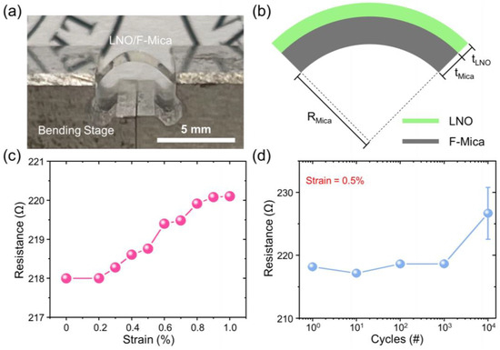
Figure 2.
(a) Digital image of a bent LNO film on the bending stage. (b) Schematic diagram of the strain calculation. Here RMica, tMica, and tLNO represent the bending radius of the mica, the mica thickness, and the LNO thickness, respectively. (c) Strain- and (d) bending cycle-dependent resistance of LNO.
Figure 2c shows the strain-dependent resistance of LNO films. It is evident that the resistance increases almost linearly with strain. The increased resistance returns to its initial value when the strain is removed. These results suggest that the electrical resistivity of LNO should be almost the same, irrespective of strain, and that the mechanical crack should not occur in LNO at least up to 1.0% strain. Mechanical cracks do not seem to occur, even after at least up to 104 repetitions of bending. Considering that the response of resistance was presented as a tangential curve in Figure 2c, we characterized the bending properties of the system under a 0.5% strain, which corresponds to the midpoint between the onset and saturation point. As shown in Figure 2d, the resistance is almost the same up to 103 repetitions of bending and slightly increased (~8.5%) up to 104 repetitions of bending.
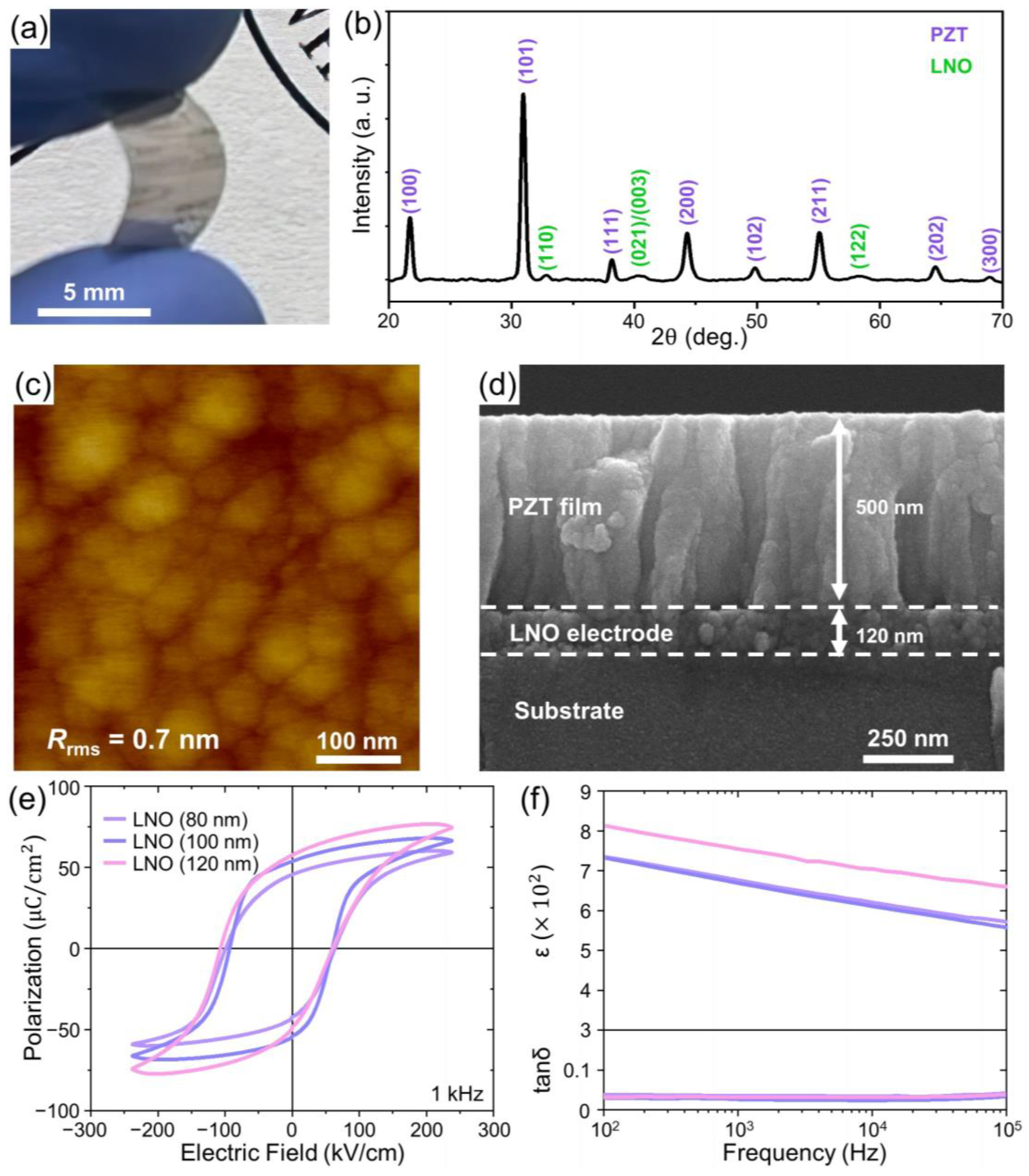
The optimized LNO bottom electrode was used to prepare the PZT film via a conventional sol-gel method. Spin-coating and crystallization were performed twice, as for the standard thickness for thick films [29]. The PZT thick films deposited on the LNO-coated F-mica substrate are highly flexible. As shown in Figure 3a, the PZT film is easily bent even by the tiny stress from human fingers.

Figure 3.
(a) Digital image of a Pb(Zr,Ti)O3 (PZT) film bent by human fingers. (b) X-ray diffraction pattern, (c) top view of atomic force microscopy, and (d) side view of scanning electron microscopy images of PZT films on LNO-coated F-mica substrate. (e) Polarization–electric field (P–E) at 1 kHz and (f) dielectric constant and loss tan δ of PZT films with different thicknesses of the LNO electrode.
Figure 3b shows the X-ray diffraction pattern of the PZT film on the LNO-coated F-mica substrate. All the diffraction peaks can be indexed as PZT (purple) and LNO (green). The peaks from F-mica are not visible, probably due to the attenuated intensity from the thick film and electrode, and the tilted substrate. Based on the diffraction pattern and Scherrer’s formula, the PZT lattice constants were estimated to be a = b = 4.076 Å and c = 4.103 Å [30], and the grain size, calculated using Scherrer’s formula based on the (101) peak of PZT, to be 21.5 nm.
Figure 3c,d show the top view of the atomic force microscopy images and the side view of the scanning electron microscopy images, respectively, of the PZT film grown on the LNO-coated F-mica substrate. The PZT film is rather smooth with a root mean square roughness of Rrms = 0.7 nm. In addition, the 500 nm thick PZT film is densely and homogeneously grown on a 120 nm thick LNO electrode. The perovskite structure of the LNO bottom electrode should greatly reduce the lattice mismatch from the monoclinic structure of F-mica, allowing the PZT film to homogeneously grow with the perovskite structure.
Figure 3e shows the polarization–electric field (P–E) curves of flexible PZT films obtained at 1 kHz. The film shows a clear square hysteresis loop with a large remnant polarization of Pr = 57.1 μC/cm2 and asymmetric coercive fields. The Pr value of the flexible PZT is quite close to that of sol-gel-grown rigid PZT of a similar chemical composition [31]. The asymmetric coercive field in flexible PZT should be related to the different amounts of oxygen vacancies near the top Pt and bottom LNO electrodes, as has been frequently reported in previous papers [32].
Remarkably, the LNO electrode affects the ferroelectric hysteresis loop of the PZT films. As clearly shown in Figure 3e, both the remnant polarization and the coercive field decrease with decreasing LNO thickness. As confirmed in Figures S4 and S5, the decreased thickness results in the decreased electrical conductivity and grain size of LNO. The decreased electrical conductivity of LNO may cause the reduced remnant polarization due to the imperfect screening of the surface charge of PZT. The reduced grain size of LNO may also cause the reduced grain size of PZT (Figure S5), which reduces the coercive field for polarization switching [33].
Figure 3f shows the dielectric constant and loss tan δ of flexible PZT films. The dielectric constant is quite high (~746 at 1 kHz) and the loss tan δ is quite low (~0.067 at 1 kHz), similar to that observed for PZT films on rigid substrates [34]. Like the P–E loop, the LNO electrode also affects the dielectric constant, rather than the loss tan δ, of PZT films. The decreased electrical conductivity of LNO should result in a reduced dielectric constant due to the reduced remnant polarization. Table 3 summarizes the LNO-thickness-dependent remnant polarization, dielectric constant at 1 kHz, and dielectric loss at 1 kHz of PZT films.
Table 3.
LNO-thickness-dependent ferroelectric and dielectric properties of flexible PZT films.
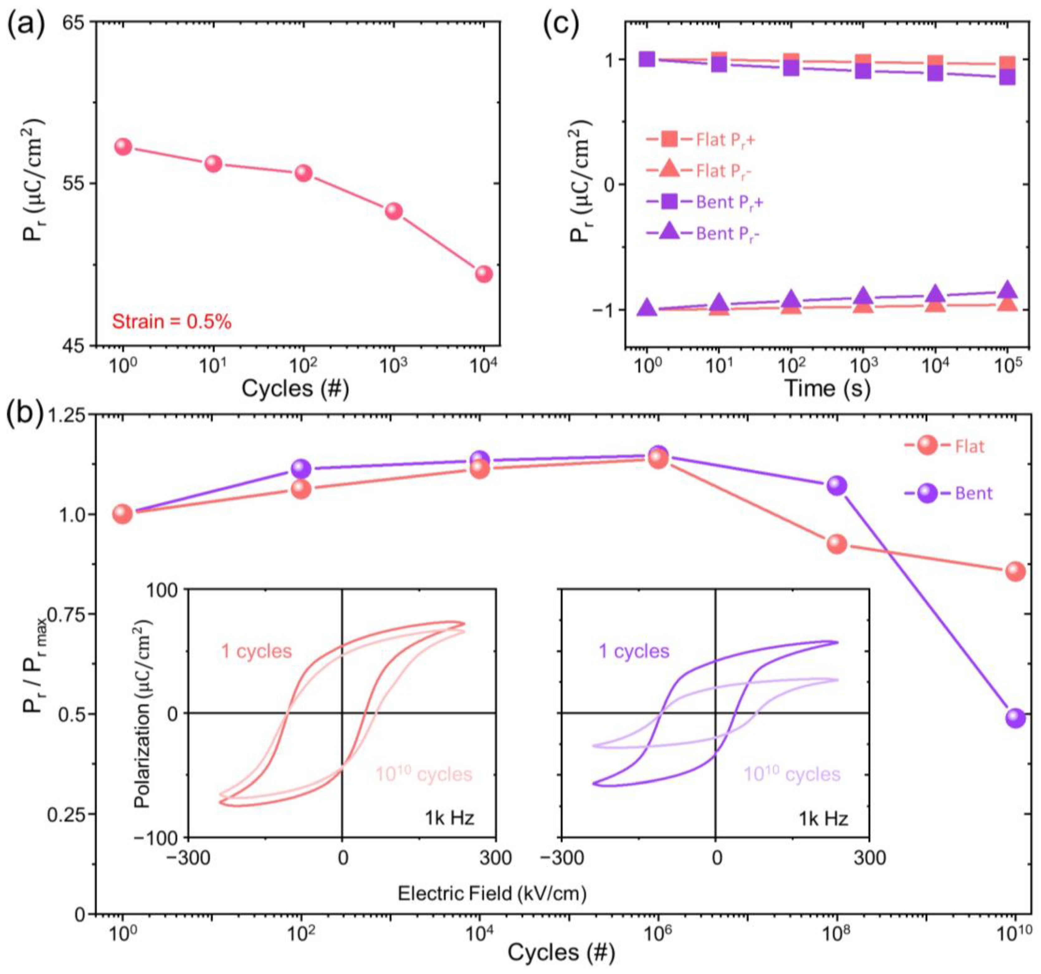
After investigating the ferroelectric and dielectric properties of flexible PZT thick films grown on LNO-coated F-mica substrate, we characterized their performance for non-volatile memory applications. Firstly, we performed a mechanical stability test of the remnant polarization under successive bending and unbending. The bending strain was fixed at 0.5%. Figure 4a shows the bending cycle-dependent Pr of flexible PZT films. The Pr value is almost constant up to 102 cycles but slightly decreases (~14%) after 104 cycles of successive bending. This result suggests that the polarization of the flexible PZT is quite stable and durable under successive mechanical bending.

Figure 4.
(a) Bending cycle-dependent remnant polarization. (b) Fatigue and (c) retention characteristics of flexible PZT films in flat and bent (convex) conditions. To characterize the imprint properties, the left and right inset of (b) present the initial and the post-1010 cycle P-E hysteresis loops under the flat and bent condition, respectively.
Next, we carried out a stability test on the remnant polarization after long-term operation. Figure 4b,c show the switching cycle and retention-time-dependent Pr of flexible PZT films. The measurements were performed in the flat and bent conditions. For the fatigue measurement, we continuously measured the P–E hysteresis loop for up to 1010 cycles. For the retention measurement, we applied a write pulse of −12 V and a read pulse of ±12 V with a width of 1 ms over a period of 105 s. The flexible PZT film in the flat state shows excellent fatigue and retention characteristics, similar to rigid films of the same composition [33]. The remnant polarization after 1010 cycles and 105 s is 81% and 96% relative to the initial values, respectively. On the other hand, the flexible PZT film in the bent state shows rather weaker fatigue and retention characteristics. Namely, the remnant polarization after 1010 cycles and 105 s is 49% and 85% relative to the initial values, respectively. However, these performances are within the acceptable range for memory applications [35].
Notably, the asymmetry of the coercive field is mitigated after long-term switching (inset of Figure 4b). The asymmetric coercive field becomes more symmetric, and these changes are evident for the bent condition. Although further studies are required, such behavior should be related to the migration of oxygen vacancies and their acceleration due to strain, as similarly observed in previous reports [36,37]. With a decrease in polarization density caused by volume distortion under the tensile stress condition, P-E behavior was influenced by the strain effect. In Table 4 and Table 5, we summarize the fatigue and retention characteristics, respectively, of the flexible PZT film under flat and bent conditions.
Table 4.
Fatigue characteristics of flexible PZT film on LNO-coated F-mica substrate under flat and bent conditions.
Table 5.
Retention characteristics of flexible PZT film on LNO-coated F-mica substrate under flat and bent conditions.
4. Summary
In summary, we systematically investigated the effects of crystallization temperature and thickness on the crystallinity, surface morphology, and electrical properties of sol-gel-grown LNO films on an F-mica substrate. The grain size and electrical resistivity are significantly varied and optimized at a crystallization temperature of 800 °C and a thickness of 120 nm. Quite smooth (a roughness of 1.7 nm), highly crystalline (a grain size of 10.2 nm), and highly conductive (a resistivity of 3.3 × 10⁻³ Ω cm) LNO film with a thickness of 120 nm is mechanically stable against 1.0% of stain and 104 repetitions of successive bending. The PZT film grown on LNO-coated F-mica substrate shows a clear hysteresis loop with a remnant polarization of 57.1 μC/cm2, a high dielectric constant of 746 at 1 kHz, and a low dielectric loss of 0.067 at 1 kHz, which are close to the values for rigid PZT film. The PZT film on the LNO-coated F-mica substrate also shows quite good ferroelectric random access memory characteristics in flat and bent conditions. The remnant polarization in the flat (bent) state is decreased to 81% (49%) after 1010 cycles in the fatigue test and 96% (85%) after 105 s in the retention test. These results suggest that the optimized LNO bottom electrode plays an important role in the application of flexible PZT film-based ferroelectric random access memory.
Supplementary Materials
The following are available online at https://www.mdpi.com/article/10.3390/cryst13121613/s1, Figure S1: synthesis flowchart of the LNO solution, Figure S2: Atomic force microscopy images (scan areas of 1 × 1 μm2) of the F-mica substrate. The right panel shows the variations of height along with the lateral (red line) and vertical (blue line) scans, Figure S3: Temperature-dependent resistivity of LNO films, grown at different crystallization temperatures. The thickness was fixed to 120 nm, Figure S4: Temperature-dependent resistivity of LNO films with different thicknesses. The crystallization temperature was fixed to 800 °C, Figure S5: The LNO-thickness-dependent X-ray diffraction pattern of PZT (101) and LNO (110). Estimated grain sizes from the Scherrer’s formula were shown for PZT and LNO.
Author Contributions
Conceptualization, J.H.J., J.H.K. and Y.U.C.; investigation and data curation, Y.U.C., H.S.A., J.E.H., D.I.Y., H.-P.L. and D.-Y.J.; writing—original draft preparation, J.H.J., J.H.K. and Y.U.C.; writing—review and editing, J.H.J., J.H.K. and M.L. All authors have read and agreed to the published version of the manuscript.
Funding
This work was supported by a National Research Foundation of Korea (NRF) grant funded by the Korea government (MSIT) (RS-2023-00207828, NRF-2023R1A2C1004159). This work was supported by a Korea Institute for Advancement of Technology (KIAT) grant funded by the Korea Government (MOTIE) (P0008458, HRD Program for Industrial Innovation). J.H.K. was supported by INHA UNIVERSITY Research Grant.
Data Availability Statement
Data are contained within the article.
Conflicts of Interest
The authors declare no conflict of interest.
References
- Jaffe, B.; Cook, W.R., Jr.; Jaffe, H. Piezoelectric Ceramics; Academic Press: London, UK, 1971. [Google Scholar]
- Xu, Y. Ferroelectric Materials and Their Applications; North-Holland: Amsterdam, The Netherlands, 1991. [Google Scholar]
- Kumar, A.; Chand, P. Pyroelectric Materials: Physics and Applications; Wiley-VCH: Weinheim, Germany, 2023. [Google Scholar]
- Miyasako, T.; Senoo, M.; Tokumitsu, E. Ferroelectric-gate thin-film transistors using indium-tin-oxide channel with large charge controllability. Appl. Phys. Lett. 2005, 86, 162902. [Google Scholar] [CrossRef]
- Muralt, P. Ferroelectric thin films for micro-sensors and actuators: A review. J. Micromech. Microeng. 2000, 10, 136–146. [Google Scholar] [CrossRef]
- Jung, J.H.; Lee, M.; Hong, J.-I.; Ding, Y.; Chen, C.-Y.; Chou, L.-J.; Wang, Z.L. Lead-free NaNbO3 nanowires for a high output piezoelectric nanogenerator. ACS Nano 2011, 5, 10041–10046. [Google Scholar] [CrossRef]
- Uchino, K. Ferroelectric Device; CRC Press: New York, NY, USA, 2009. [Google Scholar]
- Yamamoto, Y.; Harada, S.; Yamamoto, D.; Honda, W.; Arie, T.; Akita, S.; Takei, K. Printed multifunctional flexible device with an integrated motion sensor for health care monitoring. Sci. Adv. 2016, 2, e1601473. [Google Scholar] [CrossRef]
- Gao, W.; Emaminejad, S.; Nyein, H.Y.Y.; Challa, S.; Chen, K.; Peck, A.; Fahad, H.M.; Ota, H.; Shiraki, H.; Kiriya, D.; et al. Fully integrated wearable sensor arrays for multiplexed in situ perspiration analysis. Nature 2016, 529, 509–514. [Google Scholar] [CrossRef]
- Yang, J.C.; Mun, J.; Kwon, S.Y.; Park, S.; Bao, Z.; Park, S. Electronic skin: Recent progress and future prospects for skin-attachable devices for health monitoring, robotics, and prosthetics. Adv. Mater. 2019, 31, 1904765. [Google Scholar] [CrossRef]
- Yeo, H.G.; Rahn, C.; Trolier-McKinstry, S. Efficient Piezoelectric Energy Harvesters Utilizing (001) Textured Bimorph PZT Films on Flexible Metal Foils. Adv. Funct. Mater. 2016, 26, 5940–5946. [Google Scholar] [CrossRef]
- Ko, Y.J.; Kim, D.Y.; Won, S.S.; Ahn, C.W.; Kim, I.W.; Kingon, A.I.; Kim, S.-H.; Ko, J.-H.; Jung, J.H. Flexible Pb(Zr0.52Ti0.48)O3 films for a hybrid piezoelectric-pyroelectric nanogenerator under harsh environments. ACS Appl. Mater. Interfaces 2016, 8, 6504–6511. [Google Scholar] [CrossRef]
- Bitla, Y.; Chu, Y.H. MICAtronics: A new platform for flexible X-tronics. FlatChem 2017, 3, 26–42. [Google Scholar] [CrossRef]
- Lu, D.; Baek, D.J.; Hong, S.S.; Kourkoutis, L.F.; Hikita, Y.; Hwang, H.Y. Synthesis of freestanding single-crystal perovskite films and heterostructures by etching of sacrificial water-soluble layers. Nat. Mater. 2016, 15, 1255–1260. [Google Scholar] [CrossRef]
- An, F.; Qu, K.; Zhong, G.; Dong, Y.; Ming, W.; Zi, M.; Liu, Z.; Wang, Y.; Qi, B.; Ding, Z.; et al. Highly flexible and twistable freestanding single crystalline magnetite film with robust magnetism. Adv. Funct. Mater. 2020, 30, 2003495. [Google Scholar] [CrossRef]
- Kum, H.S.; Lee, H.; Kim, S.; Lindemann, S.; Kong, W.; Qiao, K.; Chen, P.; Irwin, J.; Lee, J.H.; Xie, S.; et al. Heterogeneous integration of single-crystalline complex-oxide membranes. Nature 2020, 578, 75–81. [Google Scholar] [CrossRef]
- Huang, J.; Chen, W. Flexible strategy of epitaxial oxide thin films. iScience 2022, 25, 105041. [Google Scholar] [CrossRef]
- Kingon, A.I.; Shinivasan, S. Lead zirconate titanate thin films directly on copper electrodes for ferroelectric, dielectric, and piezoelectric applications. Nat. Mater. 2005, 4, 233–237. [Google Scholar] [CrossRef]
- Jiang, J.; Bitla, Y.; Huang, C.-W.; Do, T.H.; Liu, H.-J.; Hsieh, Y.-H.; Ma, C.-H.; Jang, C.-Y.; Lai, Y.-H.; Chiu, P.-W.; et al. Flexible ferroelectric element based on van der Waals heteroepitaxy. Sci. Adv. 2017, 3, e1700121. [Google Scholar] [CrossRef]
- Xu, X.; Su, C.; Shao, Z. Fundamental Understanding and Application of Ba0.5Sr0.5Co0.8Fe0.2O3−δ Perovskite in Energy Storage and Conversion: Past, Present, and Future. Energy Fuels 2021, 35, 13585–13609. [Google Scholar] [CrossRef]
- He, J.; Xu, X.; Li, M.; Zhou, S.; Zhou, W. Recent advances in perovskite oxides for non-enzymatic electrochemical sensors: A review. Anal. Chim. Acta 2023, 1251, 341007. [Google Scholar]
- Sun, H.; Kim, H.; Xu, X.; Fei, L.; Jung, W.C.; Shao, Z. Thin Films Fabricated by Pulsed Laser Deposition for Electrocataly-sis. Renewables 2023, 1, 21–38. [Google Scholar] [CrossRef]
- Chopra, A.; Bayraktar, M.; Nijland, M.; Elshof, J.E.; Bijkerk, F.; Rijnders, G. Tuning of large piezoelectric response in nanosheet-buffered lead zirconate titanate films on glass substrates. Sci. Rep. 2017, 7, 251. [Google Scholar] [CrossRef]
- Guo, H.; Li, Z.W.; Zhao, L.; Hu, Z.; Chang, C.F.; Kuo, C.-Y.; Schmidt, W.; Piovano, A.; Pi, T.W.; Sobolev, O.; et al. Antiferromagnetic correlations in the metallic strongly correlated transition metal oxide LaNiO3. Nat. Commun. 2018, 9, 43. [Google Scholar] [CrossRef]
- Patterson, A.L. The Scherrer formula for X-ray particle size determination. Phys. Rev. 1939, 56, 978. [Google Scholar] [CrossRef]
- Scherwitzl, R.; Gariglio, S.; Zubko, P.; Gibert, M.; Triscone, J.-M. Metal-insulator transition in ultra thin LaNiO3 films. Phys. Rev. Lett. 2011, 106, 246403. [Google Scholar] [CrossRef]
- Kumar, Y.; Bhatt, H.; Prajapat, C.L.; Poswal, H.K.; Basu, S.; Singh, S. Effect of structural disorder on transport properties of LaNiO3 thin films. J. Appl. Phys. 2018, 124, 065302. [Google Scholar] [CrossRef]
- Oh, K.L.; Kwak, Y.M.; Kong, D.S.; Ryu, S.; Kim, H.; Jeen, H.; Choi, S.; Jung, J.H. Mechanical stability of ferrimagnetic CoFe2O4 flexible thin films. Curr. Appl. Phys. 2021, 31, 87–92. [Google Scholar] [CrossRef]
- Chen, J.; Teo, E.H.T.; Yao, K. Electromechanical Actuators for Haptic Feedback with Fingertip Contact. Actuators 2023, 12, 104. [Google Scholar] [CrossRef]
- Peddigari, M.; Wang, B.; Wang, R.; Yoon, W.-H.; Jang, J.; Lee, H.; Song, K.; Hwang, G.-T.; Wang, K.; Hou, Y.; et al. Giant energy density via mechanically tailored relaxor ferroelectric behavior of PZT thick film. Adv. Mater. 2023, 35, 2302554. [Google Scholar] [CrossRef]
- Wang, Y.; Ouyang, J.; Cheng, H.; Shi, Y.; Nishikado, T.; Kanno, I. High performance LaNiO3-buffered, (001)-oriented PZT piezoelectric films integrated on (111) Si. Appl. Phys. Lett. 2022, 121, 182902. [Google Scholar] [CrossRef]
- Chae, B.G.; Yang, Y.S.; Lee, S.H.; Jang, M.S.; Lee, S.J.; Kim, S.H.; Baek, W.S.; Kwon, S.C. Comparative analysis for the crystalline and ferroelectric properties of Pb(Zr,Ti)O3 thin films deposited on metallic LaNiO3 and Pt electrodes. Thin Solid Films 2002, 410, 107–113. [Google Scholar] [CrossRef]
- Liu, J.S.; Zhang, S.R.; Zeng, H.Z.; Yang, C.T.; Yuan, Y. Coercive field dependence of the grain size of ferroelectric films. Phys. Rev. B 2005, 72, 172101. [Google Scholar] [CrossRef]
- Wang, G.S.; Remiens, D.; Soyer, C. Combined annealing temperature and thickness effects on properties of PbZr0.53Ti0.47O3 films on LaNiO3/Si substrate by sol–gel process. J. Cryst. Growth 2006, 293, 370–375. [Google Scholar] [CrossRef]
- Ghoneim, M.T.; Hussain, M.M. Study of harsh environment operation of flexible ferroelectric memory integrated with PZT and silicon fabric. Appl. Phys. Lett. 2015, 107, 052904. [Google Scholar] [CrossRef]
- Fengler, F.P.G.; Pešić, M.; Starschich, S.; Schneller, T.; Künneth, C.; Böttger, U.; Mulaosmanovic, H.; Schenk, T.; Park, M.H.; Nigon, R.; et al. Domain pinning: Comparison of hafnia and PZT based ferroelectrics. Adv. Electron. Mater. 2017, 3, 1600505. [Google Scholar] [CrossRef]
- Dunn, S.; Whatmore, R.W. Substrate effects on domain structures of PZT 30/70 sol-gel films via PiezoAFM. J. Eur. Ceram. Soc. 2002, 22, 825–833. [Google Scholar] [CrossRef]

Disclaimer/Publisher’s Note: The statements, opinions and data contained in all publications are solely those of the individual author(s) and contributor(s) and not of MDPI and/or the editor(s). MDPI and/or the editor(s) disclaim responsibility for any injury to people or property resulting from any ideas, methods, instructions or products referred to in the content. |
© 2023 by the authors. Licensee MDPI, Basel, Switzerland. This article is an open access article distributed under the terms and conditions of the Creative Commons Attribution (CC BY) license (https://creativecommons.org/licenses/by/4.0/).