Abstract
Dual-wavelength output devices have a wide range of applications in mid-infrared band difference frequency generation, anti-interference lidar, dual-wavelength holographic interferometry, and other applications. Vertical external cavity surface-emitting lasers (VECSELs) are a type of semiconductor laser that can achieve single-chip dual-wavelength output by designing the chip structure. In this paper, we present a single-chip VECSEL that can switch between dual-wavelength and single-wavelength output modes. The VECSEL can simultaneously emit coaxial laser beams at 967 nm and 1013 nm, with a wavelength spacing of about 45 nm. The degree of mismatch between the gain peaks of the two quantum wells in the gain chip and the corresponding cavity modes is different. By adjusting the pump power, the temperature of the active region can be changed, which alters the matching relationship between the gain peaks and the cavity modes and controls the output mode of the VECSEL. The dual-wavelength output mode maintains a stable wavelength spacing at different operating temperatures. The laser output mode can be switched between single-wavelength and dual-wavelength, and the beam divergence angle is less than 8°. The dual-wavelength output power can exceed 400 mW, and the long-wavelength output power can reach up to 700 mW.
1. Introduction
Optically pumped vertical external-cavity surface-emitting lasers (VECSELs) combine the advantages of both semiconductor lasers and solid-state lasers, such as high output power, broad wavelength range, good beam quality, and small divergence angle [1,2,3]. The unique external cavity structure of VECSELs can effectively control the output mode of the laser and achieve a near-diffraction-limit fundamental mode beam output. The external cavity structure also facilitates the modulation of the laser output mode. Optical components such as birefringence filters, etalons, and nonlinear crystals can be inserted into the resonant cavity to perform functions such as linewidth narrowing, wavelength tuning, and frequency conversion, which greatly extend the wavelength coverage and application scenarios of VECSELs. Owing to these unique advantages, VECSELs have been widely used in frequency doubling the output of visible light, difference frequency generation mid-infrared band, sodium laser guide stars, and other fields of application [4,5,6,7,8,9].
The terahertz band possesses the benefits of low radiation energy, strong penetration, high resolution, and rich spectral information on molecular structures. It has promising application potential in medical imaging, non-destructive security inspection, in vivo detection, broadband communication, electromagnetic weapons, and other fields [10,11]. The key to the advancement of terahertz technology is the availability of low-cost and compact terahertz sources. Difference frequency generation is a relatively mature technique for producing terahertz band output [12,13,14]. VECSELs have unique advantages, such as broad wavelength range, fine wavelength tuning, and a flexible external cavity structure, making them very suitable for difference frequency generation of terahertz sources [15].
A VECSEL can employ multiple gain chips to generate two or more wavelengths in the co-axial cavity, and produce mid-infrared and terahertz band outputs through difference frequencies or sum frequencies [16,17]. Optical position meter, holographic interferometry, anti-interference lidar and other applications also require dual-wavelength-output light sources [18,19,20]. The rational design of quantum wells in VECSEL gain chips can enable dual-wavelength output of a single chip by using the two-component quantum wells or combining the single-component quantum wells with the gain-detuned cavity design [21,22]. When the gain cavity mode mismatch is large, dual-wavelength output can also be achieved [23,24]. Compared with using multiple chips to achieve dual-wavelength output, using a single chip to achieve dual-band emission is more efficient and has greater application potential. Currently, a dual-wavelength switchable output can be achieved using the single quantum well gain cavity mode large mismatch design scheme and the two-component quantum well design scheme. However, the non-radiative loss with the dual-wavelength output mode is large due to the significant gain cavity mode mismatch, which results in a decrease in the output power of VECSELs during dual-wavelength switching. To overcome this issue, the gain provided by the two-component quantum well is combined with a reasonable cavity mode mismatch design. This allows for second-wavelength lasing to be achieved before the power is reduced due to excessive mismatch between the first wavelength and the cavity mode. As a result, a power drop during dual-wavelength output is avoided, and a more stable wavelength switching output is achieved.
Hence, this study developed a VECSEL with a single chip to achieve a flexible switching dual-wavelength output. Two-component quantum wells with different output wavelengths were placed into a single gain chip, and the quantum wells were located at the amplitude positions of the corresponding standing waves. Through the reasonable mismatch design of the cavity mode and the two gain peaks, the stable power output of the dual-wavelength switching was achieved. The dual-wavelength operation maintained almost the same wavelength interval at different temperatures.
2. System Overview
Figure 1 illustrates the dual-wavelength gain chip structure and the VECSEL system structure. The entire dual-wavelength output system adopted a linear cavity VECSEL configuration, which consisted of four components: an output coupling mirror, a gain chip, a heat dissipation system, and a pump system. As shown in Figure 1, a dual-wavelength output was achieved in a simple linear cavity, with a wavelength spacing of approximately 45 nm. The intracavity laser oscillation mode was adjusted by varying the cavity length between the output coupling mirror and the gain chip. The output coupling mirror was a flat-concave mirror with a curvature radius of 5 cm, and the reflectivity in the dual-wavelength band was about 97.5%. The chip was designed as an optical pumping structure, which uses a light absorption layer to absorb the pump light and generate photogenerated carriers for injection into the active region. The pump’s light source was a fiber-coupled diode laser with a wavelength of 808 nm and a maximum power of 100 W. The optical absorption layer was able to effectively absorb the laser wavelength at 808 nm. The focusing mirror group at the output end controlled the output spot size to achieve good pump area control. The pump angle was inclined at approximately 40°.
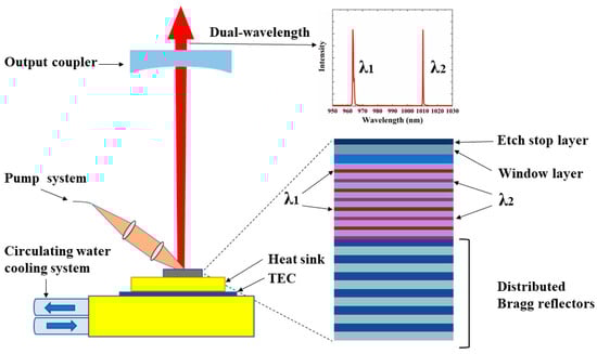
Figure 1.
Schematic of the working principle in the dual-wavelength VECSEL.
The gain chip employed a bottom-emitting structure, where a buffer layer was first grown on a GaAs substrate, followed by an etching stop layer, window layer, multi-quantum well structure, and finally a distributed Bragg reflector (DBR) [25]. The DBR of the gain chip of the bottom emitting structure was exposed to the outside. The metal layer was evaporated on the DBR for metallization, and then welded to the heat sink for rapid heat extraction. The gain chip was bonded on the copper radiator, which was mounted on a heat dissipation base with a thermoelectric cooler (TEC). TEC regulated the working temperature of the laser, and the circulating water-cooling system removed the waste heat generated by the studio. The circulating water-cooling system was set at 20 °C. After the bonding of the gain chip was complete, the bottom of the gain surface needed to be removed to expose the light port. The substrate removal process consisted of two phases: mechanical thinning and chemical etching. In the first phase, a thinning machine was utilized to decrease the thickness of the substrate to about 100 μm. In the second phase, the residual substrate was eliminated by applying a chemical etchant. The etchant used a ratio of 1:20 of ammonia and hydrogen peroxide. The GaInP etching stop layer was not easily corroded by the etchant, and was used to protect the gain chip structure from damage during the etching process.
The structure of the gain chip is shown in the illustration in Figure 1. The top layer of the gain chip structure after stripping is the GaInP etching stop layer, followed by the AlGaAs window layer. The active region is located between the window layer and the DBR. The quantum well in the active region comprises two material components, namely, the five short-wavelength In0.15GaAs QW, with a gain peak of 930 nm, and the five long-wavelength In0.22GaAs QW, with a gain peak of 980 nm. The thicknesses of the two types of quantum wells were both 6 nm. By adjusting the thickness of the barrier layer, the quantum wells were positioned at the corresponding standing wave peak positions and each other’s standing wave nodes, so as to achieve high gain while avoiding the absorption of each other’s gain [22,26]. DBR was formed by alternating the stacking of GaAs and AlAs, with a reflectivity of 99.99% in the dual-wavelength band.
3. Experimental Results
The gain chip structure was grown on a GaAs (100) substrate using the Aixtron 200/4 MOCVD system, followed by an etching stop layer, window layer, active region, and DBR structure. The etching barrier layer used 30 nm of GaInP material to protect the gain chip structure during the removal of the substrate. The window layer used a half-wavelength thick AlGaAs material to avoid carrier escape to the surface for non-radiative recombination. The active region comprised two sets of InGaAs quantum wells (QWs), with thicknesses of 6 nm each. The quantum wells were separated by an intermediate GaAs barrier layer of about 100 nm, which also functioned as a light absorption layer. In the process of material epitaxial growth, there was a compressive strain effect in the InGaAs quantum wells, and the higher the In concentration, the greater the compressive strain effect. Therefore, GaAsP with the opposite strain effect was introduced for strain compensation to achieve good material growth quality. GaAsP material layers of about 20 nm were placed on both sides of the GaAs layer to compensate for the strain effect of the quantum wells, while inhibiting the escape of the photogenerated carriers produced by the light absorption layer to other regions. After the growth of the active region structure material, 30 pairs of quarter-wavelength GaAs/AlAs DBR structures were grown.
Figure 2a shows the reflection spectrum of VECSEL after the removal of the substrate. The reflection spectrum revealed a high-reflectivity band with a width of approximately 100 nm near the dual-wavelength region. Within the band, there were two distinct dips, which corresponded to the F-P cavity modes induced by the Fabry–Perot resonance effect of the gain chip structure, indicating the laser emission positions of the VECSEL [27]. The first F-P cavity mode was located at 966 nm, and the second F-P cavity mode was located at 1010 nm, representing the emission wavelengths of the VECSEL. Figure 2b shows the photoluminescence (PL) spectra measured from the edge and plane positions of the chip. After the epitaxial growth of the gain chip structure, there was no material layer blocking at the edge of the chip after cleavage, and the gain spectrum generated by the quantum well could be directly measured. The photoluminescence spectrum measured at the edge of the chip was the intrinsic gain of the quantum well without cavity mode modification. The photoluminescence spectrum of the quantum well without cavity mode modification had two obvious main peaks at 930 nm and 977 nm, respectively, which were close to the gain peak of the designed quantum well. This proved that the quantum well structure after strain compensation in the epitaxial growth process had good growth quality and no obvious material defects. The gain spectrum after F-P cavity mode modification is shown in Figure 2b, with gain peaks located at 962 nm and 1006 nm. The gain peak measured on the plane of the gain chip matched the cavity mode, and the laser achieved optimal output at this wavelength. As the temperature increased, the material gain and refractive index underwent significant changes, resulting in a red shift of the quantum well gain peak and a red shift of the cavity mode position. The temperature drift velocity of the quantum well gain peak was almost three times that of the cavity mode position [28]. Thus, as the operating temperature of the VECSEL increased, the output mode of the laser gradually shifted towards the second wavelength, achieving wavelength switching.
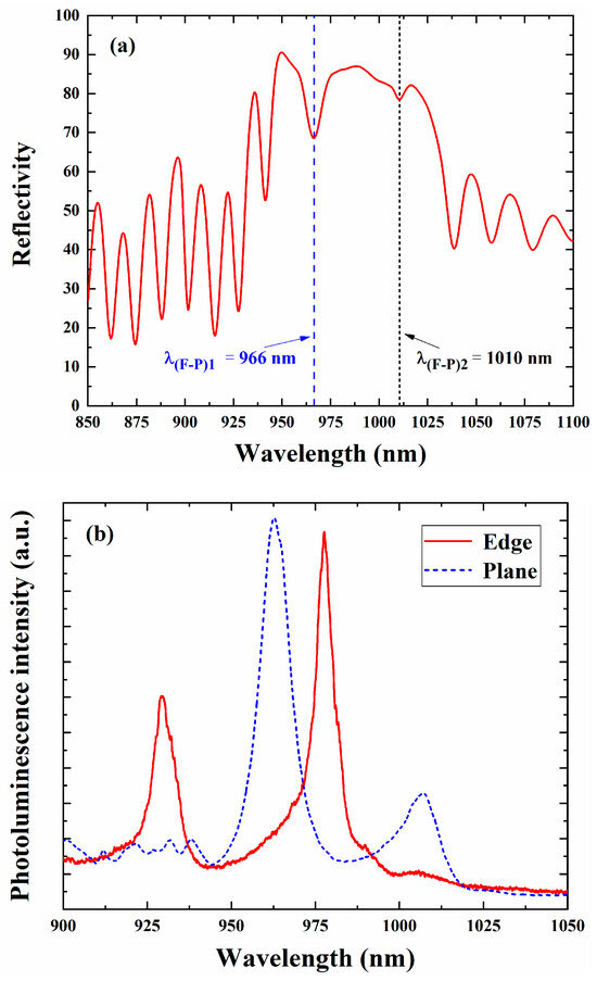
Figure 2.
(a) Gain chip reflection spectrum at 20 °C. (b) Photoluminescence spectra obtained at the edge and plane of the gain chip at 20 °C.
The VECSEL device was mounted on the base of the thermal dissipation system, and an external cavity system was constructed for testing. The cooling temperature of the circulating water was set to 20 °C for the evaluation of the VECSEL’s performance. Figure 3 illustrates the power curves of the VECSEL at TEC temperatures of −5, 0, and 5 °C. The figure clearly shows the region where the slope efficiency decreased between two linear regions. As the pump power increased, the short wavelength mode reached the threshold pump power first, resulting in laser emission, and the output power gradually increased. The pump power continued to increase; the long-wavelength mode reached the threshold pump power, resulting in dual-wavelength emission; and the slope efficiency of the power curve decreased. There was carrier competition between the two modes, and the short-wavelength cavity mode had a gain peak cavity mode mismatch due to a rise in temperature, resulting in a decrease in slope efficiency. As the pump power continued to increase, the short-wavelength mode became excessively detuned, resulting in the cessation of the short-wavelength emission and leaving only the long-wavelength emission. The slope efficiency increased until the power curve underwent a thermal rollover. As the pump power continued to increase, the temperature of the active region became too high, resulting in a significant mismatch between the long-wavelength gain and the cavity mode, as well as an increase in non-radiative recombination. The active region produced more waste heat accumulation, forming a vicious cycle. The output power of the VECSEL decreased with the increase in pump power, a phenomenon called power thermal rollover. The output power of the dual-wavelength mode was more than 400 mW, and the maximum output power of the long-wavelength mode was more than 700 mW.
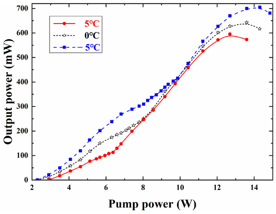
Figure 3.
VECSEL output power curves at different operating temperatures.
Figure 4 depicts the wavelength change of the region where the slope efficiency dropped in the power curve, that is, the switching of the two wavelength output modes. The TEC temperature was maintained at 0 °C; five points were taken in the region where the slope efficiency decreased in the power curve; and the wavelengths corresponding to the VECSEL output were measured. The pump power of the VECSEL wavelength switching output in Figure 4 was taken from the region where the slope efficiency of the power curve at 0 °C decreased in Figure 3, that is, the pump power was between 6.2 W and 8.3 W. The pump power was 6.3 W, and the VECSEL output was a single-wavelength emission with a wavelength of 965.1 nm. At this point, the pump power had not yet reached the threshold for the long-wavelength lasing. As the pump power increased, the temperature of the active region in the pump center gradually increased, and the drift of the gain peak gradually matched the long wavelength cavity mode until the pump power reached the long-wavelength output threshold. At a pump power of 6.95 W, VECSEL achieved dual-wavelength simultaneous lasing output, with a spacing of approximately 45 nm between the two wavelengths. The long wavelength was located at 1011.7 nm, close to the second F-P cavity mode. The pump power continued to increase, causing excessive redshift of the short wavelength gain peak. This resulted in a mismatch between the gain peak and the cavity mode, as well as a decrease in the mode intensity of the short wavelength. The intensity of the long-wavelength output mode increased. At a pump power of 7.15 W, the output intensities of the two wavelengths of VECSEL were almost equal. The pump power continued to increase, the short-wavelength output intensity continued to decrease, and the long-wavelength output intensity continued to increase. At a pump power of 8.3 W, due to the excessive gain detuning, the short wavelength ceased to emit, and the VECSEL output mode was a single-wavelength long wave. Due to the high temperature in the active region, the long wavelength drifted to 1013.9 nm.
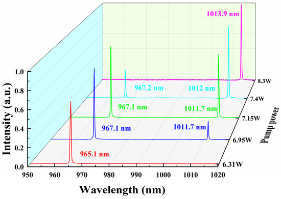
Figure 4.
Variation in lasing wavelength with pump power at 0 °C.
Figure 5 depicts the dual wavelength and the corresponding pump threshold of VECSEL as a function of temperature. At different operating temperatures, the threshold pump power of the two output wavelengths under the same conditions was recorded. The threshold pump power of the short wavelength was the threshold pump power of VECSEL, which increased with the increase in temperature. This was attributed to the temperature rise that enhanced the non-radiative recombination and the carrier loss, resulting in a lower gain of the quantum well. The threshold pump power of the long wavelength decreased with the increase in temperature. As the operating temperature increased, the temperature drift coefficient of the gain peak was larger than that of the cavity mode, and the significant mismatch between the long-wavelength gain peak and the cavity mode was reduced, resulting in a decrease in threshold pump power. The figure also shows the change in the wavelength of the simultaneous output of the two wavelengths, which had a wavelength interval of about 45 nm at different operating temperatures. The device performance of the VECSEL was very stable, and it was able to maintain a stable wavelength interval at different operating temperatures.
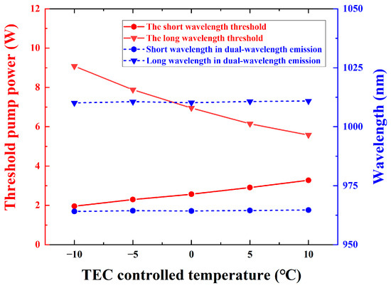
Figure 5.
Dual wavelength and corresponding pump threshold of the VECSEL varied with temperature.
Figure 6 illustrates the far-field patterns of the VECSEL output modes with short, dual, and long wavelengths at 0 °C. The far-field patterns exhibit Gaussian profiles in both dimensions for all output wavelengths. The inset in the top left corner of the figure depicts the 2D beam profile captured by a charge-coupled device (CCD), which showed a circular shape with a uniform intensity distribution. As the pump power increased, the output mode of the laser switched, but the beam profile remained circular and uniform. The divergence angles were 7.0°, 7.4°, and 7.7° for the short-, dual-, and long-wavelength output modes, respectively. The divergence angle at different propagation distances was less than 8°. This indicates that the different output modes of the VECSEL originated from the same region of the active layer with the same optical axis, and that the output performance was stable.
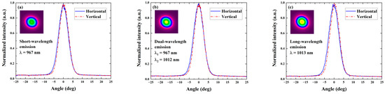
Figure 6.
One-dimensional far-field modes of VECSEL were measured under different output modes: (a) short-wavelength, (b) dual-wavelength, and (c) long-wavelength. The beam profiles of the VECSEL are shown in the inset images.
4. Conclusions
We present a VECSEL with switchable dual-wavelength output based on two types of quantum well structures in the gain chip and the corresponding cavity mode matching mechanism. The quantum wells of the two components provided gains at peaks of 930 nm and 980 nm, respectively, which matched the two Fabry–Perot cavity modes. The detuning between the two cavity modes and the gain peaks was different, and the temperature coefficient of the gain peaks was larger than that of the cavity modes. By controlling the pump power, we were able to affect the operating temperature of the active region and achieve switchable laser output modes. The operating temperature of the active region was calculated by measuring the peak drift of the edge PL spectrum. We demonstrated wavelength switching between 967 nm and 1013 nm, with a stable wavelength interval of about 45 nm. The dual-wavelength output power of the VECSEL was greater than 400 mW. The divergence angle of the VECSEL was less than 8° for different output modes, and it showed negligible change when the output mode switched, confirming that the two wavelengths were coaxial. This coaxial output single-chip dual-wavelength VECSEL with a small size, low divergence angle, and high power would be very suitable for difference frequency generation terahertz, anti-jamming radar, and other applications.
In our future work, we will focus on the design of a small and compact modular laser system which can achieve coaxial dual-wavelength switchable output by adjusting the pump power. We will also provide a novel light source option for a current differential frequency generation terahertz source, anti-interference lidar, and other applications.
Author Contributions
Project supervision, Y.N., L.W. and J.Z. (Jianwei Zhang); chip design, J.Z. (Jianwei Zhang), Z.Z., X.Z. and C.C.; external cavity design, Z.Z. and Y.Z.; reflection spectrum measurement, Z.Z., T.L. and Z.D.; external cavity debugging, Z.Z., Z.D., J.Z. (Jiye Zhang) and T.L.; comprehensive system performance test, Z.Z., J.Z. (Jianwei Zhang), T.L. and H.B.; analysis and discussion of experimental results, Z.Z., J.Z. (Jiye Zhang), J.Z. (Jianwei Zhang), C.C. and Y.Z.; writing—first draft preparation, Z.Z.; writing review and editing, J.Z. (Jianwei Zhang); funding acquisition, J.Z. (Jianwei Zhang), Y.N., L.Q. and L.W. All authors have read and agreed to the published version of the manuscript.
Funding
This work was funded by the National Natural Science Foundation of China (Grant nos. 62104225 and 62274165), the Key Scientific and Technological Research Projects in Jilin Province (Grant nos. 20220201066GX and 20220201077GX), and the Major Program of National Natural Science Foundation of China (Grant no. 62090060).
Institutional Review Board Statement
Not applicable.
Informed Consent Statement
Not applicable.
Data Availability Statement
Experimental data are available upon reasonable request to the authors.
Conflicts of Interest
The authors declare no conflict of interest.
References
- Mangold, M.; Wittwer, V.J.; Sieber, O.D.; Hoffmann, M.; Krestnikov, I.L.; Livshits, D.A.; Golling, M.; Südmeyer, T.; Keller, U. VECSEL gain characterization. Opt. Express 2012, 20, 4136–4148. [Google Scholar] [CrossRef] [PubMed]
- Guina, M.; Rantamäki, A.; Härkönen, A. Optically pumped VECSELs: Review of technology and progress. J. Phys. D Appl. Phys. 2017, 50, 383001. [Google Scholar] [CrossRef]
- Rahimi-Iman, A. Recent advances in VECSELs. J. Opt. 2016, 18, 093003. [Google Scholar] [CrossRef]
- Kahle, H.; Bek, R.; Heldmaier, M.; Schwarzbäck, T.; Jetter, M.; Michler, P. High optical output power in the UVA range of a frequency-doubled, strain-compensated AlGaInP-VECSEL. Appl. Phys. Express 2014, 7, 092705. [Google Scholar] [CrossRef]
- Tropper, A.C.; Foreman, H.D.; Garnache, A.; Wilcox, K.G.; Hoogland, S.H. Vertical-external-cavity semiconductor lasers. J. Phys. D Appl. Phys. 2004, 37, R75–R85. [Google Scholar] [CrossRef]
- Kantola, E.; Leinonen, T.; Ranta, S.; Tavast, M.; Guina, M. High-efficiency 20 W yellow VECSEL. Opt. Express 2014, 22, 6372–6380. [Google Scholar] [CrossRef] [PubMed]
- Tilma, B.W.; Mangold, M.; Zaugg, C.A.; Link, S.M.; Waldburger, D.; Klenner, A.; Mayer, A.S.; Gini, E.; Golling, M.; Keller, U. Recent advances in ultrafast semiconductor disk lasers. Light Sci. Appl. 2015, 4, e310. [Google Scholar] [CrossRef]
- Zhang, F.; Gaafar, M.; Moller, C.; Stolz, W.; Koch, M.; Rahimi-Iman, A. Dual-Wavelength Emission from a Serially Connected Two-Chip VECSEL. IEEE Photon-Technol. Lett. 2016, 28, 927–929. [Google Scholar] [CrossRef]
- Huo, X.; Qi, Y.; Zhang, Y.; Chen, B.; Bai, Z.; Ding, J.; Wang, Y.; Lu, Z. Research development of 589 nm laser for sodium laser guide stars. Opt. Lasers Eng. 2020, 134, 106207. [Google Scholar] [CrossRef]
- Siegel, P. Terahertz technology. IEEE Trans. Microw. Theory Tech. 2002, 50, 910–928. [Google Scholar] [CrossRef]
- Pawar, A.Y.; Sonawane, D.D.; Erande, K.B.; Derle, D.V. Terahertz technology and its applications. Drug Invent. Today 2013, 5, 157–163. [Google Scholar] [CrossRef]
- Lewis, R.A. A review of terahertz sources. J. Phys. D Appl. Phys. 2014, 47, 374001. [Google Scholar] [CrossRef]
- Liu, P.; Niu, C.; Qi, F.; Li, W.; Li, W.; Fu, Q.; Guo, L.; Li, Z. Phase-Matching in Nonlinear Crystal-Based Monochromatic Terahertz-Wave Generation. Crystals 2022, 12, 1231. [Google Scholar] [CrossRef]
- Ezhov, D.; Turgeneva, S.; Nikolaev, N.; Mamrashev, A.; Mikerin, S.; Minakov, F.; Simanchuk, A.; Antsygin, V.; Svetlichnyi, V.; Losev, V.; et al. Potential of Sub-THz-Wave Generation in Li2B4O7 Nonlinear Crystal at Room and Cryogenic Temperatures. Crystals 2021, 11, 1321. [Google Scholar] [CrossRef]
- Scheller, M.; Paul, J.R.; Laurain, A.; Young, A.; Koch, S.W.; Moloney, J.V. Terahertz generation by difference frequency conversion of two single-frequency VECSELs in an external resonance cavity. In Proceedings of the SPIE LASE, Vertical External Cavity Surface Emitting Lasers (VECSELs) IV, San Francisco, CA, USA, 1–6 February 2014; Volume 8966. [Google Scholar] [CrossRef]
- Ni, Y.; Hu, Q.; Wu, H.; Han, W.; Yu, X.; Mao, M. The Investigation on Mid-Far Infrared Nonlinear Crystal AgGaGe5Se12 (AGGSe). Crystals 2021, 11, 661. [Google Scholar] [CrossRef]
- Mamrashev, A.; Nikolaev, N.; Antsygin, V.; Andreev, Y.; Lanskii, G.; Meshalkin, A. Optical Properties of KTP Crystals and Their Potential for Terahertz Generation. Crystals 2018, 8, 310. [Google Scholar] [CrossRef]
- Muszalski, J.; Broda, A.; Trajnerowicz, A.; Wójcik-Jedlińska, A.; Sarzała, R.P.; Wasiak, M.; Gutowski, P.; Sankowska, I.; Kubacka-Traczyk, J.; Gołaszewska-Malec, K. Switchable double wavelength generating vertical external cavity surface-emitting laser. Opt. Express 2014, 22, 6447–6452. [Google Scholar] [CrossRef] [PubMed]
- Petrov, V.; Pogoda, A.; Sementin, V.; Sevryugin, A.; Shalymov, E.; Venediktov, D.; Venediktov, V. Advances in Digital Holographic Interferometry. J. Imaging 2022, 8, 196. [Google Scholar] [CrossRef] [PubMed]
- Zhihua, P.; Chengtian, S.; Bohu, L.; Xiaowen, W.; Mengqian, D.; Hong, S. Accurate Ranging of Dual Wavelength FMCW Laser Fuze Under Different Types of Aerosol Interference. IEEE Sens. J. 2022, 22, 18953–18960. [Google Scholar] [CrossRef]
- Morozov, Y.; Leinonen, T.; Harkonen, A.; Pessa, M. Simultaneous Dual-Wavelength Emission from Vertical External-Cavity Surface-Emitting Laser: A Numerical Modeling. IEEE J. Quantum Electron. 2006, 42, 1055–1061. [Google Scholar] [CrossRef]
- Zhuo, Z.; Jianwei, Z.; Jiye, Z.; Yugang, Z.; Jun, Z.; Yinli, Z.; Xing, Z.; Li, Q.; Yun, L.; Yongqiang, N.; et al. Switchable two-wavelength emission using vertical external-cavity surface-emitting laser. Optik 2022, 264, 169409. [Google Scholar] [CrossRef]
- Zhang, J.; Zhang, J.; Zhang, Z.; Zeng, Y.; Zhang, X.; Zhu, H.; Huang, Y.; Qin, L.; Ning, Y.; Wang, L.; et al. High-power vertical external-cavity surface-emitting laser emitting switchable wavelengths. Opt. Express 2020, 28, 32612–32619. [Google Scholar] [CrossRef] [PubMed]
- Jasik, A.; Sokół, A.K.; Broda, A.; Sankowska, I.; Wójcik-Jedlińska, A.; Wasiak, M.; Kubacka-Traczyk, J.; Muszalski, J. Dual-wavelength vertical external-cavity surface-emitting laser: Strict growth control and scalable design. Appl. Phys. B Laser Opt. 2016, 122, 1–8. [Google Scholar] [CrossRef]
- Wang, T.-L.; Heinen, B.; Hader, J.; Dineen, C.; Sparenberg, M.; Weber, A.; Kunert, B.; Koch, S.; Moloney, J.; Koch, M.; et al. Quantum design strategy pushes high-power vertical-external-cavity surface-emitting lasers beyond 100 W. Laser Photon-Rev. 2012, 6, L12–L14. [Google Scholar] [CrossRef]
- Morozov, Y.A.; Nefedov, I.S.; Leinonen, T.; Morozov, M.Y. Nonlinear-optical frequency conversion in a dual-wavelength vertical-external-cavity surface-emitting laser. Semiconductors 2008, 42, 463–469. [Google Scholar] [CrossRef]
- Yang, H.-P.D.; Lu, C.; Hsiao, R.; Chiou, C.; Lee, C.; Huang, C.; Yu, H.; Wang, C.; Lin, K.; Maleev, N.A.; et al. Characteristics of MOCVD- and MBE-grown InGa(N)As VCSELs. Semicond. Sci. Technol. 2005, 20, 834–839. [Google Scholar] [CrossRef][Green Version]
- Tropper, A.; Hoogland, S. Extended cavity surface-emitting semiconductor lasers. Prog. Quantum Electron. 2006, 30, 1–43. [Google Scholar] [CrossRef]
Disclaimer/Publisher’s Note: The statements, opinions and data contained in all publications are solely those of the individual author(s) and contributor(s) and not of MDPI and/or the editor(s). MDPI and/or the editor(s) disclaim responsibility for any injury to people or property resulting from any ideas, methods, instructions or products referred to in the content. |
© 2023 by the authors. Licensee MDPI, Basel, Switzerland. This article is an open access article distributed under the terms and conditions of the Creative Commons Attribution (CC BY) license (https://creativecommons.org/licenses/by/4.0/).