Abstract
Despite the increasing interest in graphene, a less studied aspect is the enhancement of silicon (Si) performances due to the interaction with graphene-based materials. In this study, cyclic voltammetry and electric impedance measurements are performed on graphene oxide (GO) dip-coated on n-type and p-type Si samples. The electrical properties of GO on n-type Si samples are dramatically enhanced: The conductivity and the photocurrent meaningfully increase in comparison to bare n-type Si. Such findings could be used in a wide variety of optoelectronic applications, improving GO future applicability in the Si semiconductor industry.
1. Introduction
The semiconductor technology is based on crystalline silicon (Si), which is an inefficient light-emitting material because it is an indirect bandgap semiconductor [1]. Therefore, attention in the semiconductor field has turned to graphene, which is a single layer of carbon atoms arranged in a honeycomb lattice [2] that has ultrahigh charge-carrier mobility, broadband light absorption, and linear dispersion band structure [3]. Graphene is thus an advantageous material for several applications in electronics and optoelectronics [4,5].
Despite its outstanding properties, graphene cannot replace Si entirely because of the poor on/off current ratio, which results from its zero bandgap [6]. However, it has been suggested that graphene could improve Si-based devices to afford broadband operation in light routing and amplification in components such as polarizers, modulators, and photodetectors [6].
Another advantage of graphene-based materials is that they can be produced in ultrathin sheet form that can be transferred to suitable substrates [7].
Graphene oxide (GO) is a graphene-based material that has more oxygen-containing groups and defects compared with mechanically exfoliated or chemical vapor-deposited graphene. These defects are proven to be favorable to enhancing the performance of photodetectors [8]. Furthermore, previous research works have shown that GO thin films have high optical transmittance in the visible region of the spectrum that allows their use as protective coatings and optically transparent electrodes, crucial in solar cells and for optical applications [9].
GO has been studied for several applications [10,11,12,13,14,15,16,17,18,19,20,21,22,23,24] in previous research works.
In particular, Brzhezinskaya et al. [25] demonstrated a simple method for GO deposition for creating different electronic devices including memristor devices for neuromorphic computing systems in the field of large data and artificial intelligence. Khurana et al. [26] observed thermally stable bipolar resistive switching behavior in the memory devices composed of GO thin films on indium tin oxide coated glass substrate with platinum as the top electrode. Panin et al. [27] reported resistive switching behaviors in an Al/GO/Al planar structure. Qi et al. [28] demonstrated highly uniform resistive switching and a high on/off ratio of resistive random access memory based on GO by embedding gold nanoparticles into the device. Jeong et al. [28] presented a GO-based memory that can be easily fabricated using a room-temperature spin-casting method on flexible substrates and has reliable memory performance in terms of retention and endurance.
In our works, we have studied the optical properties of GO [9,29]. A less studied aspect in the framework of graphene-based material is the enhancement of Si performances due to the interaction with GO.
In this work, we characterize GO thin films deposited on n-type and p-type Si substrates using cyclic voltammetry and impedance measurements. The photocurrent and conductivity of n-type Si are substantially enhanced due to the interaction with GO thin films, which could be crucial for several applications in the optical field.
2. Materials and Methods
The n-type and p-type Si wafers used as substrates were ultrasonically cleaned in acetone, then in bidistilled water, and finally in isopropanol.
All samples were prepared using GO 2 g/L dispersion in H2O (bought from Punto Quantico).
The dip-coating process [30] was used to deposit GO films (10 nm) on n-type and p-type Si with a homemade apparatus at a speed of 0.33 mm/s.
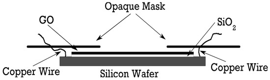
Figure 1.
Scheme of the sample cell.
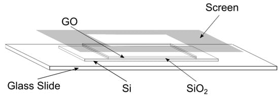
Figure 2.
Scheme of the sample cell.
The ends of the silicon strip were etched with a hydrogen fluoride solution to remove the native SiO2 layer, and two copper conductors were indium soldered on both ends. An opaque mask reduced the light-exposed surface of the sample to an area of 17 mm × 5 mm.
In Figure 3, the photos of the sample cell are reported.
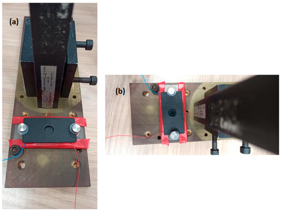
Figure 3.
Photos of the sample cell. (a) front view (b) top view.
In Figure 4, the scheme of the experimental setup is reported.
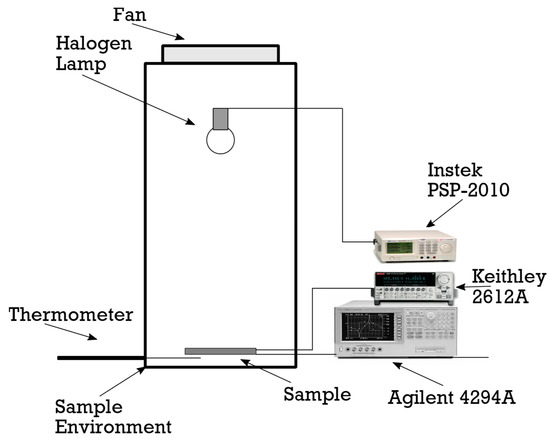
Figure 4.
Experimental setup.
The sample was placed inside an insulated dark box, the temperature of which was controlled by a fan and a thermometer. The light beam was emitted by a tungsten halogen lamp powered at a constant current of 8.3A (100 W) using an Instek 2010 PSP-2010 power supply. Current-to-voltage scans were performed using a Keithley 2612A source meter. Sample impedance was measured using an Agilent 4294A Precision Impedance Analyzer. All the measurements were made at room temperature and were performed inside the dark box in conditions of dark and light illumination (4450 lux).
Additional morphological, optical, and electrical measurements of the samples are available in the Supplementary Materials.
3. Results and Discussion
In Figure 5 and Figure 6, the cyclic voltammetry measurements of n-type (p-type) Si and GO/n-type (p-type) Si samples under dark and light illumination conditions are reported.
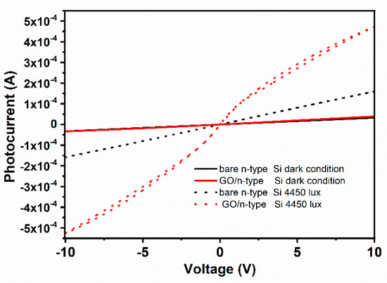
Figure 5.
Cyclic voltammetry measurements on n-type silicon and graphene oxide/n-type Si samples under dark and light illumination conditions.
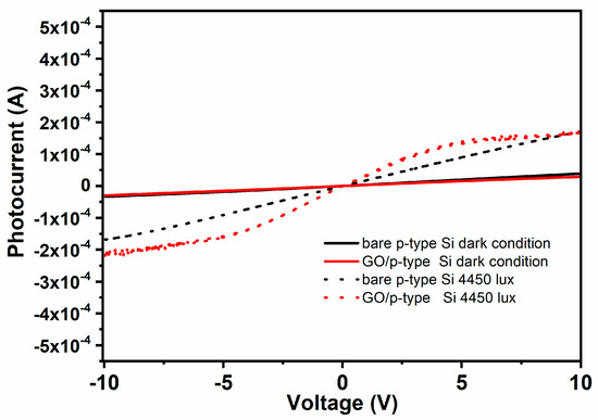
Figure 6.
Cyclic voltammetry measurements on p-type silicon and graphene oxide/p-type Si samples under dark and light illumination conditions.
As can be seen in Figure 5, the I–V characteristics show that the photocurrent of the GO/n-type Si samples more than tripled in comparison to bare n-type Si samples under light illumination.
Under light illumination conditions, incident light is absorbed in the Si substrate and electron−hole pairs are generated as a result. Therefore, an explanation of the observed behavior may be that photogenerated carriers in GO can be driven toward the Si conduction band by a built-in electrical field with light illumination. At the same time, Si also absorbs photons and excites the photogenerated carriers. Electrons will accumulate in the conduction band of Si, while photogenerated holes will be transported into the GO’s valence band. The mechanism of generation and transportation inhibits the effective recombination of carriers, and in turn, increases the photocurrent.
The I–V characteristics in Figure 6 reveal a current behavior in the GO/p-type Si samples almost identical to that of the bare p-type Si in dark and light illumination conditions. Therefore, there is no substantial improvement due to the presence of GO in the case of p-type Si substrates.
Figure 7 and Figure 8 show the impedance measurements on n-type (p-type) Si and GO/n-type (p-type) Si samples.
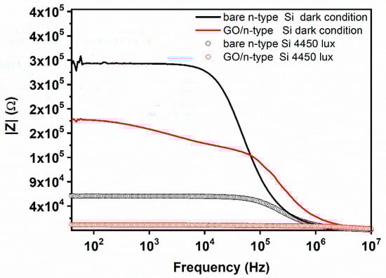
Figure 7.
Impedance measurements on n-type silicon and graphene oxide/n-type Si samples under dark and light illumination conditions.
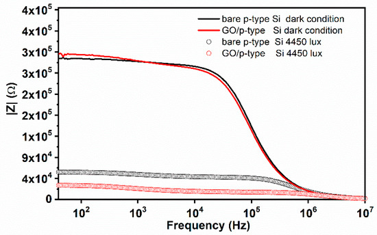
Figure 8.
Impedance measurements on p-type silicon and graphene oxide/p-type Si samples under dark and light illumination conditions.
In Figure 7, the impedance of GO/n-type Si samples decreases in both the absence and presence of light radiation. The conductivity is quintupled for GO/n-type Si samples in comparison to bare n-type Si under light conditions.
A possible explanation may be that GO doping shifts the Fermi energy level of Si towards the Si conduction band, thus increasing its conductivity. However, additional research is required to corroborate this claim.
As shown in Figure 8, the p-type silicon and GO/p-type Si samples have the same impedance behavior in dark conditions. In the presence of light radiation, there is an increase in GO/p -type Si conductivity in comparison to bare p-type Si.
4. Conclusions
In summary, this study provides a demonstration of an innovative method for improving the conductivity of Si using GO.
The photocurrent and conductivity of n-type Si are significantly enhanced by dip-coating GO on it. The photocurrent of p-type Si is not significantly affected by interaction with GO, whereas its conductivity is enhanced.
Hence, GO could improve the Si semiconductor industry, (especially n-type Si), finding applications in numerous areas such as solar cells, touch screens, transparent displays, imaging, sensing, and other optoelectronic applications.
Supplementary Materials
The following supporting information can be downloaded at: https://www.mdpi.com/article/10.3390/cryst13010073/s1, Figure S1: Scanning electron microscopy image of GO films on Si substrates (n-type). Figure S2: Scanning electron microscopy image of GO films on Si substrates (p-type). Figure S3: Particle size distribution of very diluted GO flakes in water. Figure S4: Variable angle spectroscopic ellipsometry measurements of graphene oxide films on Si substrates (n-type). Experimental and model generated ψ (a) and Δ (b) data fit at different angles of incidence. Figure S5: Variable angle spectroscopic ellipsometry measurements of graphene oxide films on Si substrates (p-type). Experimental and model generated ψ (a) and Δ (b) data fit at different angles of incidence. Figure S6: Impedance measurements on n-type Si and graphene oxide/n-type Si samples under dark and light illumination conditions. Figure S7: Cyclic voltammetry measurements on n-type Si and graphene oxide/n-type Si samples under dark and light illumination conditions.
Author Contributions
Investigation, G.G.P., S.B. and C.V.; supervision, C.V.; writing—original draft preparation, G.G.P. and C.V.; writing—review and editing, G.G.P. and C.V. All authors have read and agreed to the published version of the manuscript.
Funding
This research received no external funding.
Data Availability Statement
Not applicable.
Conflicts of Interest
The authors declare no conflict of interest.
References
- Hirschman, K.D.; Tsybeskov, L.; Duttagupta, S.P.; Fauchet, P.M. Silicon-based visible light-emitting devices integrated into microelectronic circuits. Nature 1996, 384, 338. [Google Scholar] [CrossRef]
- Geim, A.K.; Novoselov, K.S. The rise of graphene. Nat. Mater. 2007, 6, 183–191. [Google Scholar] [CrossRef]
- Castriota, M.; Politano, G.G.; Vena, C.; De Santo, M.P.; Desiderio, G.; Davoli, M.; Cazzanelli, E.; Versace, C. Variable Angle Spectroscopic Ellipsometry investigation of CVD-grown monolayer graphene. Appl. Surf. Sci. 2019, 467–468, 213–220. [Google Scholar] [CrossRef]
- Hsieh, Y.-P.; Yen, C.-H.; Lin, P.-S.; Ma, S.-W.; Ting, C.-C.; Wu, C.-I.; Hofmann, M. Ultra-high sensitivity graphene photosensors. Appl. Phys. Lett. 2014, 104, 41110. [Google Scholar] [CrossRef]
- Callicó, G.M. Image sensors go broadband. Nat. Photonics 2017, 11, 332. [Google Scholar] [CrossRef]
- Kim, K.; Choi, J.-Y.; Kim, T.; Cho, S.-H.; Chung, H.-J. A role for graphene in silicon-based semiconductor devices. Nature 2011, 479, 338. [Google Scholar] [CrossRef]
- Yi, M.; Shen, Z. A review on mechanical exfoliation for the scalable production of graphene. J. Mater. Chem. A 2015, 3, 11700–11715. [Google Scholar] [CrossRef]
- Zhu, M.; Li, X.; Guo, Y.; Li, X.; Sun, P.; Zang, X.; Wang, K.; Zhong, M.; Wu, D.; Zhu, H. Vertical junction photodetectors based on reduced graphene oxide/silicon Schottky diodes. Nanoscale 2014, 6, 4909–4914. [Google Scholar] [CrossRef]
- Politano, G.G.; Versace, C.; Vena, C.; Castriota, M.; Ciuchi, F.; Fasanella, A.; Desiderio, G.; Cazzanelli, E. Physical investigation of electrophoretically deposited graphene oxide and reduced graphene oxide thin films. J. Appl. Phys. 2016, 120, 195307. [Google Scholar] [CrossRef]
- Nguyen, Q.K.; Kuz’micheva, G.M.; Khramov, E.V.; Svetogorov, R.D.; Chumakov, R.G.; Cao, T.T. Design of Metal-Organic Polymers MIL-53(M3+): Preparation and Characterization of MIL-53(Fe) and Graphene Oxide Composite. Crystals 2021, 11, 1281. [Google Scholar] [CrossRef]
- Perumal, D.; Albert, E.L.; Saad, N.; Hin, T.Y.; Zawawi, R.M.; Teh, H.F.; Che Abdullah, C.A. Fabrication and Characterization of Clinacanthus nutans Mediated Reduced Graphene Oxide Using a Green Approach. Crystals 2022, 12, 1539. [Google Scholar] [CrossRef]
- Zhou, S.; Zhang, X.; Zhou, H.; Li, D. Effects of Graphene Oxide Encapsulated Silica Fume and Its Mixing with Nano-Silica Sol on Properties of Fly Ash-Mixed Cement Composites. Crystals 2022, 12, 144. [Google Scholar] [CrossRef]
- Politano, G.G.; Versace, C. Variable Angle Spectroscopic Ellipsometry Characterization of Graphene Oxide in Methanol Films. Crystals 2022, 12, 696. [Google Scholar] [CrossRef]
- Wang, X.; Lu, S.; Xu, W. Synthesis of Needle-like Nanostructure Composite Electrode of Co3O4/rGO/NF for High-Performance Symmetric Supercapacitor. Crystals 2022, 12, 664. [Google Scholar] [CrossRef]
- Alshoaibi, A.; Awada, C.; Ahmed, F.; Obodo, R.M.; Maaza, M.; Ezema, F.I. Trimetallic Oxides/GO Composites Optimized with Carbon Ions Radiations for Supercapacitive Electrodes. Crystals 2022, 12, 874. [Google Scholar] [CrossRef]
- Wang, S.; Wang, X.; He, J.; Xin, M. Mechanical Behavior and Microstructure of Graphene Oxide Electrodeposited Carbon Fiber Reinforced Cement-Based Materials. Crystals 2022, 12, 964. [Google Scholar] [CrossRef]
- Abo-Dief, H.M.; Alanazi, A.K.; Alothman, Z.A.; Pramanik, T.; Mohamed, A.T.; Fallata, A.M.; Althakafy, J.T. An Investigation into the Production of rGO/CuO Composites Using Plant Wastes. Crystals 2022, 12, 1423. [Google Scholar] [CrossRef]
- Alanazi, A.K.; Abo-Dief, H.M.; Alothman, Z.A.; Mohamed, A.T.; Pramanik, T.; Fallata, A.M. Effect of rGO wt.% on the Preparation of rGO/CuO Nanocomposites at Different Test Periods and Temperatures. Crystals 2022, 12, 1325. [Google Scholar] [CrossRef]
- Kashif, M.; Alsaiari, N.S.; Jaafar, E.; Low, F.W.; Oon, C.S.; Sahari, S.K.; Almuaikel, N.S. Reaction-Time-Dependent Opto-Electrical Properties of Graphene Oxide. Crystals 2022, 12, 1303. [Google Scholar] [CrossRef]
- Politano, G.G.; Versace, C. Electrical and Optical Characterization of Graphene Oxide and Reduced Graphene Oxide Thin Films. Crystals 2022, 12, 1312. [Google Scholar] [CrossRef]
- Xu, X.; Xiong, C.; Mao, S.; Yao, W. Established Model on Polycrystalline Graphene Oxide and Analysis of Mechanical Characteristic. Crystals 2022, 12, 382. [Google Scholar] [CrossRef]
- Ansari, A.R.; Ansari, S.A.; Parveen, N.; Ansari, M.O.; Osman, Z. Silver Nanoparticle Decorated on Reduced Graphene Oxide-Wrapped Manganese Oxide Nanorods as Electrode Materials for High-Performance Electrochemical Devices. Crystals 2022, 12, 389. [Google Scholar] [CrossRef]
- Riley, P.R.; Joshi, P.; Penchev, H.; Narayan, J.; Narayan, R.J. One-Step Formation of Reduced Graphene Oxide from Insulating Polymers Induced by Laser Writing Method. Crystals 2021, 11, 1308. [Google Scholar] [CrossRef]
- Shireesha, K.; Kumar, T.R.; Rajani, T.; Chakra, C.S.; Kumari, M.M.; Divya, V.; Raghava Reddy, K. Novel NiMgOH-rGO-Based Nanostructured Hybrids for Electrochemical Energy Storage Supercapacitor Applications: Effect of Reducing Agents. Crystals 2021, 11, 1144. [Google Scholar] [CrossRef]
- Brzhezinskaya, M.; Kapitanova, O.O.; Kononenko, O.V.; Koveshnikov, S.; Korepanov, V.; Roshchupkin, D. Large-scalable graphene oxide films with resistive switching for non-volatile memory applications. J. Alloys Compd. 2020, 849, 156699. [Google Scholar] [CrossRef]
- Khurana, G.; Misra, P.; Katiyar, R.S. Forming free resistive switching in graphene oxide thin film for thermally stable nonvolatile memory applications. J. Appl. Phys. 2013, 114, 124508. [Google Scholar] [CrossRef]
- Panin, G.N.; Kapitanova, O.O.; Lee, S.W.; Baranov, A.N.; Kang, T.W. Resistive Switching in Al/Graphene Oxide/Al Structure. Jpn. J. Appl. Phys. 2011, 50, 70110. [Google Scholar] [CrossRef]
- Qi, M.; Cao, S.; Yang, L.; You, Q.; Shi, L.; Wu, Z. Uniform multilevel switching of graphene oxide-based RRAM achieved by embedding with gold nanoparticles for image pattern recognition. Appl. Phys. Lett. 2020, 116, 163503. [Google Scholar] [CrossRef]
- Politano, G.G.; Vena, C.; Desiderio, G.; Versace, C. Spectroscopic ellipsometry investigation of the optical properties of graphene oxide dip-coated on magnetron sputtered gold thin films. J. Appl. Phys. 2018, 123, 55303. [Google Scholar] [CrossRef]
- Scriven, L.E. Physics and Applications of DIP Coating and Spin Coating. MRS Proc. 1988, 121, 717. [Google Scholar] [CrossRef]


Disclaimer/Publisher’s Note: The statements, opinions and data contained in all publications are solely those of the individual author(s) and contributor(s) and not of MDPI and/or the editor(s). MDPI and/or the editor(s) disclaim responsibility for any injury to people or property resulting from any ideas, methods, instructions or products referred to in the content. |
© 2023 by the authors. Licensee MDPI, Basel, Switzerland. This article is an open access article distributed under the terms and conditions of the Creative Commons Attribution (CC BY) license (https://creativecommons.org/licenses/by/4.0/).