
Study on Deposition Conditions in Coupled Polysilicon CVD Furnaces by Simulations

Abstract
:1. Introduction
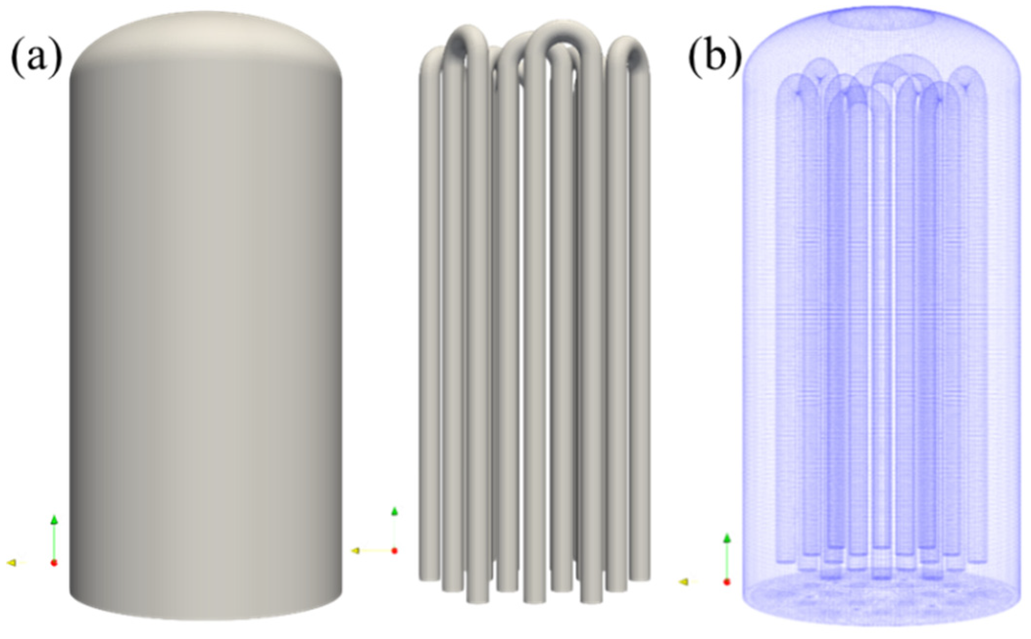
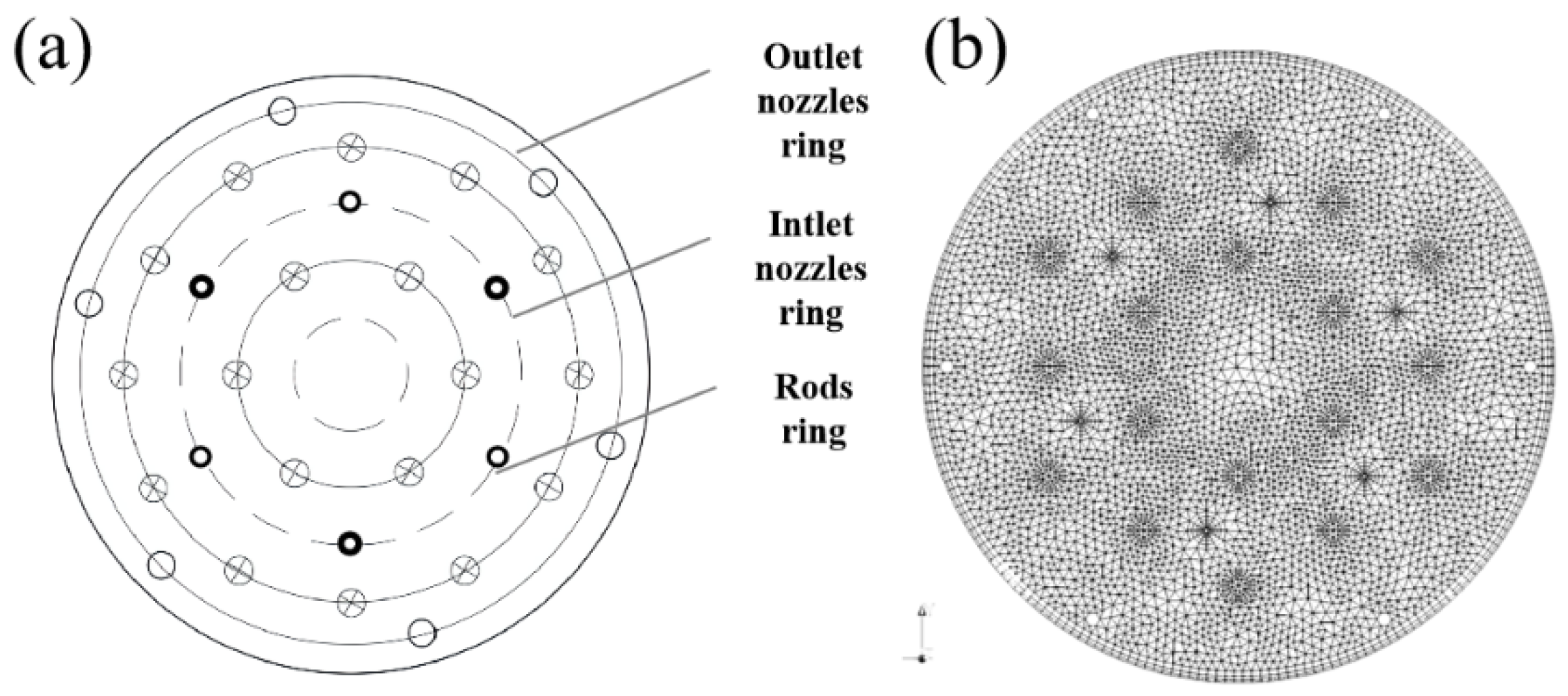
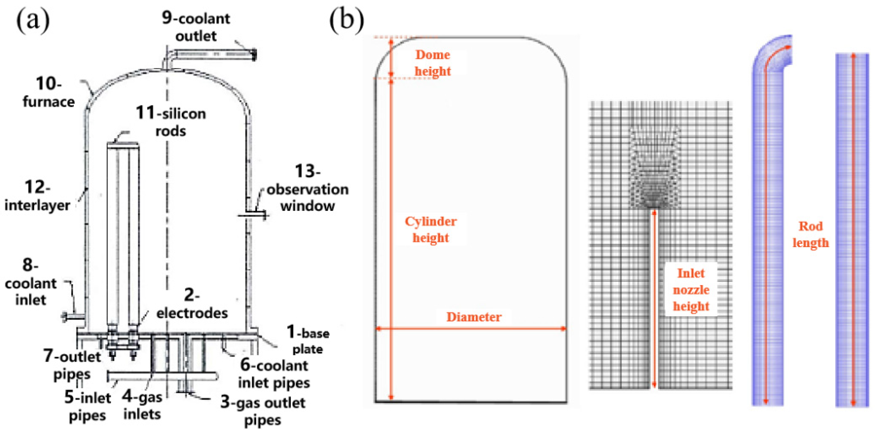
2. Modeling Process
3. Results and Discussion
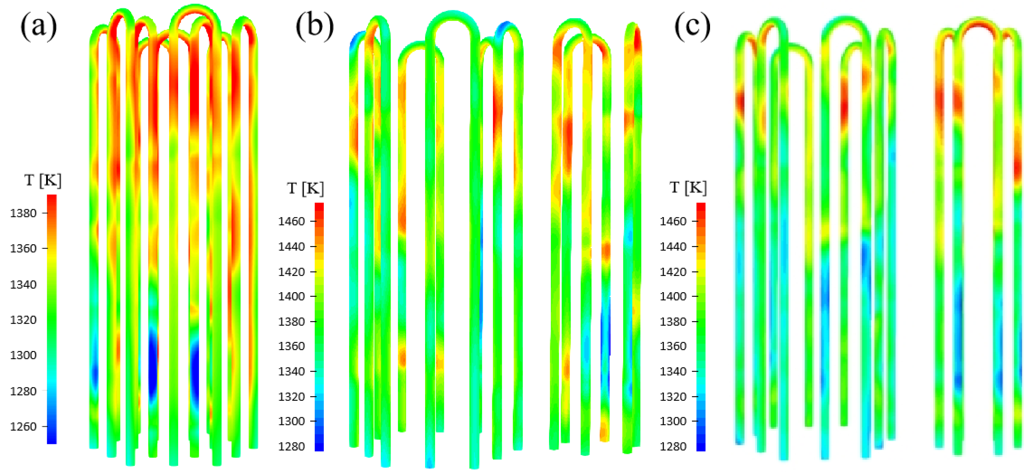
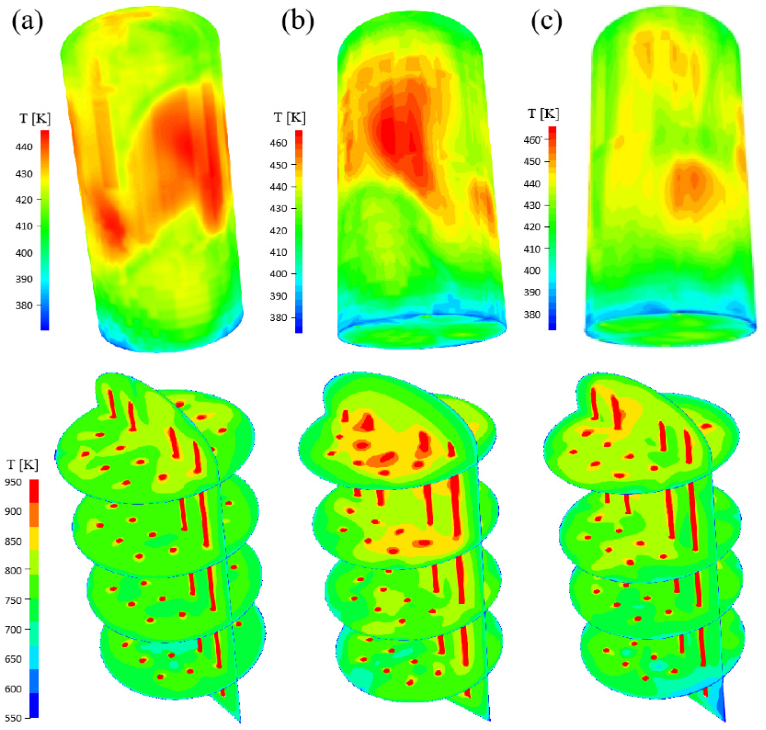
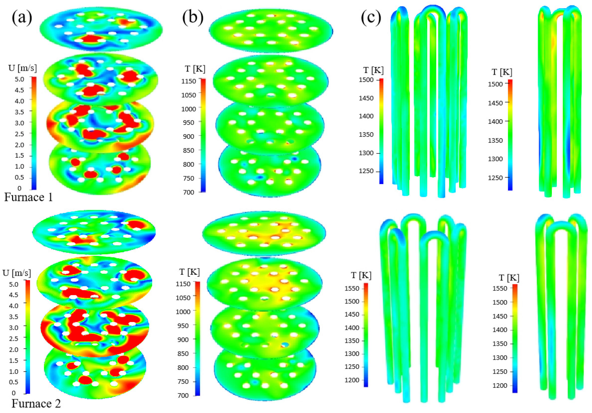
3.1. Temperature Distribution
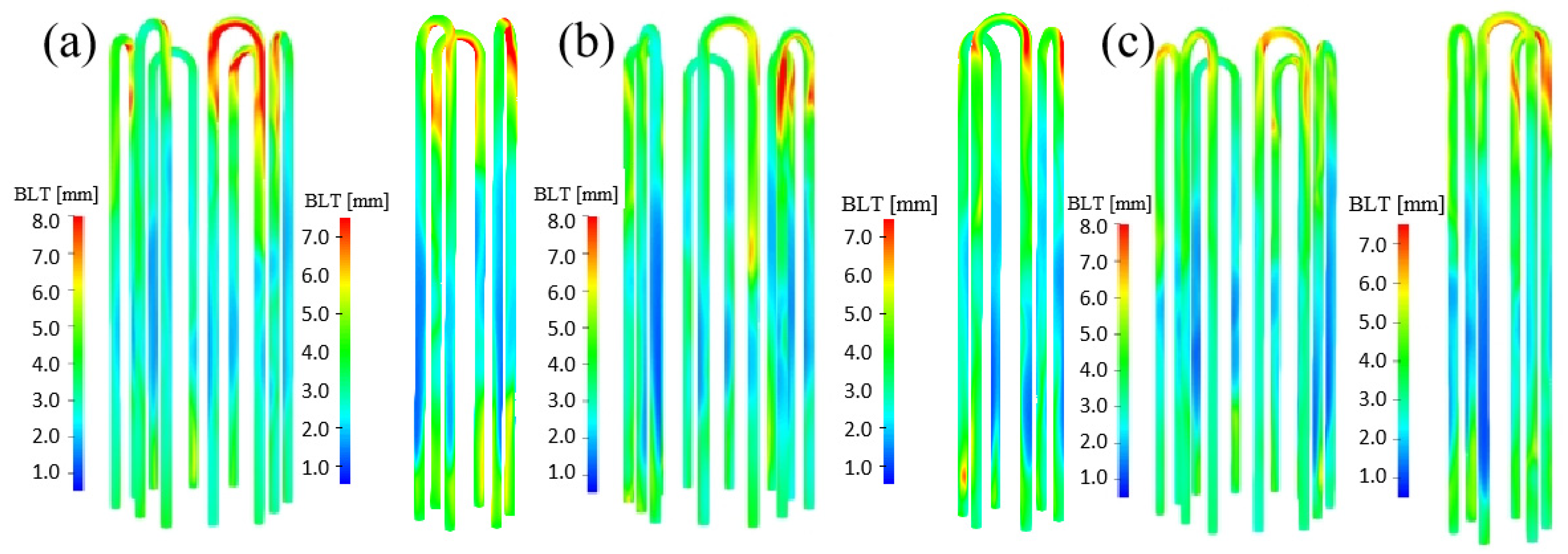
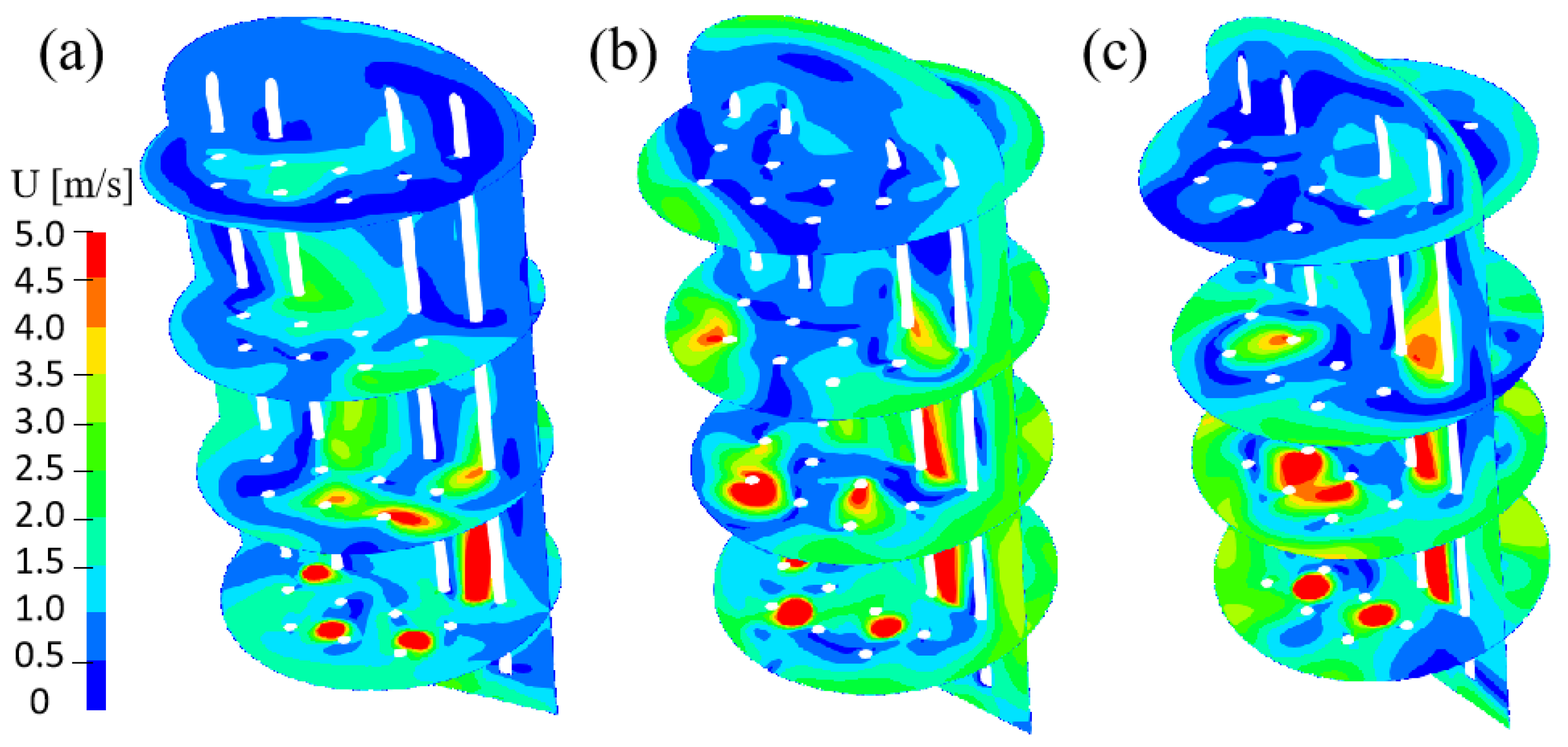
3.2. Surface Velocity and Boundary Layer Thickness of Silicon Rods
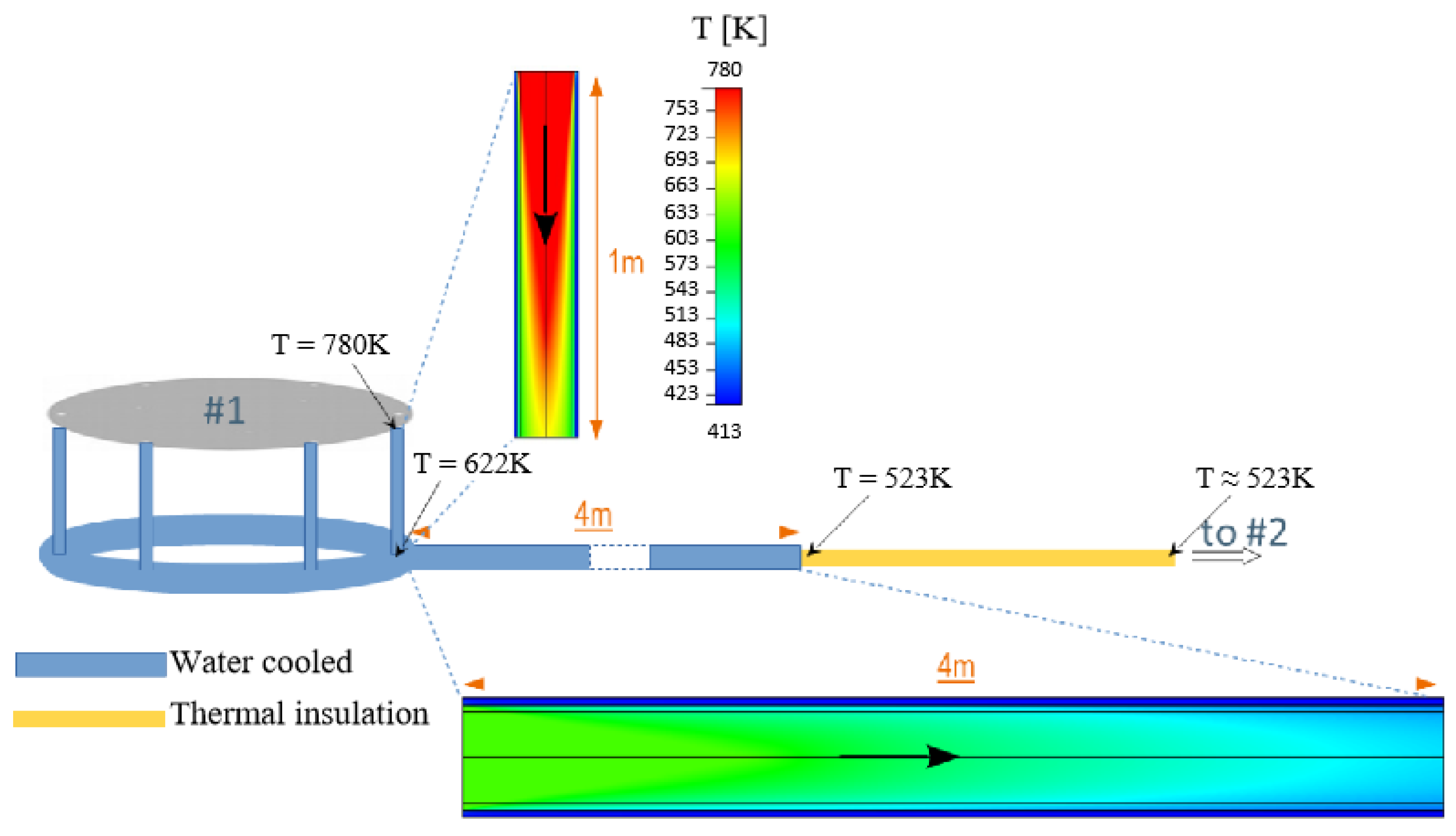
3.3. Results of Coupling Scheme
4. Conclusions
Author Contributions
Funding
Institutional Review Board Statement
Informed Consent Statement
Acknowledgments
Conflicts of Interest
References
- Ramirez-Marquez, C.; Otero, M.V.; Vazquez-Castillo, J.A.; Martin, M.; Segovia-Hernandez, J.G. Process design and intensification for the production of solar grade silicon. J. Clean. Prod. 2018, 170, 1579–1593. [Google Scholar] [CrossRef]
- Trinh, A.-K.; González, I.; Fournier, L.; Pelletier, R.; Sandoval, V.J.C.; Lesage, F.J. Solar thermal energy conversion to electrical power. Appl. Therm. Eng. 2014, 70, 675–686. [Google Scholar] [CrossRef]
- Reznichenko, M. Evolution of Requirements for Solar Grade Silicon. Procedia Eng. 2016, 139, 41–46. [Google Scholar] [CrossRef]
- Li, X.-G.; Xiao, W.-D. Model on transport phenomena and control of rod growth uniformity in siemens CVD reactor. Comput. Chem. Eng. 2018, 117, 351–358. [Google Scholar] [CrossRef]
- Bye, G.; Ceccaroli, B. Solar grade silicon: Technology status and industrial trends. Sol. Energy Mater. Sol. Cells 2014, 130, 634–646. [Google Scholar] [CrossRef]
- del Coso, G.; del Cañizo, C.; Luque, A. Chemical Vapor Deposition Model of Polysilicon in a Trichlorosilane and Hydrogen System. J. Electrochem. Soc. 2008, 155, 485–491. [Google Scholar] [CrossRef]
- Fang, M.; Xiong, Y.Y.; Yuan, X.Z.; Liu, Y.W. Numerical Analysis of the Chemical Vapor Deposition of Polysilicon in a Trichlorosilane and Hydrogen System. In International Conference on Applied Energy, Icae2014; Yan, J., Lee, D.J., Chou, S.K., Desideri, U., Li, H., Eds.; Elsevier Ltd.: Taipei, Taiwan, 2014; pp. 1987–1991. [Google Scholar]
- Wang, Z.; Wei, W. External cost of photovoltaic oriented silicon production: A case in China. Energy Policy 2017, 107, 437–447. [Google Scholar] [CrossRef]
- Pizzini, S. Towards solar grade silicon: Challenges and benefits for low cost photovoltaics. Sol. Energy Mater. Sol. Cells 2010, 94, 1528–1533. [Google Scholar] [CrossRef]
- Yadav, S.; Chattopadhyay, K.; Singh, C.V. Solar grade silicon production: A review of kinetic, thermodynamic and fluid dynamics based continuum scale modeling. Renew. Sustain. Energy Rev. 2017, 78, 1288–1314. [Google Scholar] [CrossRef]
- Nie, Z.; Ramachandran, P.A.; Hou, Y. Optimization of effective parameters on Siemens reactor to achieve potential maximum deposition radius: An energy consumption analysis and numerical simulation. Int. J. Heat Mass Transf. 2018, 117, 1083–1098. [Google Scholar] [CrossRef]
- Vallerio, M.; Claessens, D.; Logist, F.; Van Impe, J. Multi-Objective and Robust Optimal Control of a CVD Reactor for Polysilicon Production. In Computer Aided Chemical Engineering; Klemes, J.J., Varbanov, P.S., Liew, P.Y., Eds.; Elsevier: Amsterdam, The Netherlands, 2014; pp. 571–576. [Google Scholar]
- Luo, X.; Li, S.; Li, G.; Xie, Y.-C.; Zhang, H.; Huang, R.-Z.; Li, C.-J. Cold Spray (CS) Deposition of a Durable Silver Coating with High Infrared Reflectivity for Radiation Energy Saving in the Polysilicon CVD Reactor. Surf. Coat. Technol. 2021, 409, 126841. [Google Scholar] [CrossRef]
- Nie, Z.; Wang, Y.; Wang, C.; Guo, Q.; Hou, Y.; Ramachandran, P.A.; Xie, G. Mathematical Model and Energy Efficiency Analysis of Siemens Reactor with a Quartz Ceramic Lining. Appl. Therm. Eng. 2021, 199, 117522. [Google Scholar] [CrossRef]
- Sun, Q.; Chen, H.; Duan, C.; Wan, Y. Effect of Reaction Temperature and Mixture Ratio on Polysilicon Production Process. In International Conference on Advanced Materials, Processing and Testing Technology; Trans Tech Publications, Ltd.: Guangzhou, China, 2021. [Google Scholar]
- Nie, Z.; Zhou, Y.; Deng, J.; Wen, S.; Hou, Y. Thermal and Electrical Behavior of Silicon Rod with Varying Radius in a 24-Rod Siemens Reactor Considering Skin Effect and Wall Emissivity. Int. J. Heat Mass Transf. 2017, 111, 1142–1156. [Google Scholar] [CrossRef]
- Du, P.; Zhou, Y.; Ramachandran, P.A.; Xie, G.; Hou, Y. Numerical Investigations of Heat Transfer and Skin Effect Characteristics within Rods Located in a 48-Rod Siemens Reactor Heated by AC. Appl. Therm. Eng. 2021, 193, 116972. [Google Scholar] [CrossRef]
- An, L.-S.; Liu, C.-J.; Liu, Y.-W. Optimization of operating parameters in polysilicon chemical vapor deposition reactor with response surface methodology. J. Cryst. Growth 2018, 489, 11–19. [Google Scholar] [CrossRef]
- Ramos, A.; Rodríguez, A.; del Cañizo, C.; Valdehita, J.; Zamorano, J.C.; Luque, A. Heat losses in a CVD reactor for polysilicon production: Comprehensive model and experimental validation. J. Cryst. Growth 2014, 402, 138–146. [Google Scholar] [CrossRef]
- Tang, G.; Chen, C.; Cai, Y.; Zong, B.; Cai, Y.; Wang, T. Numerical Simulations of a 96-rod Polysilicon CVD Reactor. J. Cryst. Growth 2018, 489, 68–71. [Google Scholar]
- Xin, Y.; Shao-fen, W.; Da-zhou, Y. Three-dimensional Numerical Simulation and Optimization of Polysilicon Reduction Furnace Based on Fluent. Energy Sav. Nonferrous Metall. 2011, 27, 48–52+56. [Google Scholar]
- Shimin, L.; Shengtao, Z.; Yinfeng, H.; Min, H. Research on improvement of flow structure of electronic polysilicon reduction furnace based on numerical simulation. J. Synth. Cryst. 2019, 48, 545–549. [Google Scholar]
- Yu, C.; Zhou, Y.M.; Du, P.; Zhao, L.; Zhao, D.; Wang, P.J.; Tian, L.; Xie, G.; Hou, Y.Q. Alternating Current Heating Model of Rods Located in Siemens Reactor. Fuel Cells 2021, 21, 11–17. [Google Scholar] [CrossRef]


| Categories | Parameters (mm) |
|---|---|
| Reactor height | 2500 |
| Chamber height | 320 |
| Reactor diameter | 1400 |
| Outlet diameter | 35 |
| Silicon rod height | 2300 |
| Typical silicon rod diameter | 50 |
| Schemes | Electric Current (A) | Temperature of Wall (K) | Temperature of Feed Gas (K) | Operating Pressure (kPa) | TCS Flow kg/h | DCS/TCS % | H2/Si |
|---|---|---|---|---|---|---|---|
| Design A | 1480 | 370 | 393 | 600 | 550 | 3 | 3.24 |
| Design B | 1480 | 370 | 393 | 600 | 550 | 3 | 3.24 |
| Design C | 1480 | 370 | 393 | 600 | 1375 | 3 | 3.24 |
| Categories | Parameters | |
|---|---|---|
| Emissivity | Silicon rods | 0.76 |
| Furnace wall | 0.36 | |
| Base plate | 0.36 | |
| Heat Conductivity (W/(m·K)) | Furnace wall | 17 |
| Base plate | 17 | |
| Rod Diameter | Design A | Design B | Design C |
|---|---|---|---|
| 50 mm | 47.8 | 53 | 51.8 |
| 90 mm | 45.3 | 48 | 44.1 |
| 125 mm | - | 48.9 | 48.1 |
| Average value | 46.6 | 50.0 | 48.0 |
| Rod Diameter | Tail Gas Temperature | Furnace #1 Pipe Outlet Temperature | Furnace #2 Pipe Outlet Temperature |
|---|---|---|---|
| 30 mm | 646 | 472 | 534 |
| 50 mm | 780 | 523 | 622 |
| 90 mm | 1025 | 582 | 749 |
| 125 mm | 1028 | 573 | 745 |
| Rod Diameter | Furnace #1 | Furnace #2 | Difference |
|---|---|---|---|
| 50 mm | 51.8 | 52.3 | 0.5 |
| 90 mm | 44.1 | 45.0 | 0.9 |
| 125 mm | 48.1 | 48.2 | 0.1 |
| Parameters | Design A | Furnace #1 | Furnace #2 | Coupling Mode | Optimization Proportion |
|---|---|---|---|---|---|
| Deposition rate (kg/h) | 14.08 | 21.4 | 19.4 | 20.4 | 44.9% |
| Unit energy consumption (kWh/kg) | 89.6 | 66.6 | 82.5 | 74.2 | 17.2% |
| Conversion rate (%) | 12 | 7.37 | 7.22 | 14.1 | 17.5% |
| Process time (h) | 79.8 | 52.6 | 52.6 | 52.6 | 34.1% |
| Total output (kg) | 1124 | 1124 | 1020 | 1072 | 4.6% |
Publisher’s Note: MDPI stays neutral with regard to jurisdictional claims in published maps and institutional affiliations. |
© 2022 by the authors. Licensee MDPI, Basel, Switzerland. This article is an open access article distributed under the terms and conditions of the Creative Commons Attribution (CC BY) license (https://creativecommons.org/licenses/by/4.0/).
Share and Cite
Zhang, S.; Fu, H.; Fan, G.; Li, T.; Han, J.; Zhao, L. Study on Deposition Conditions in Coupled Polysilicon CVD Furnaces by Simulations. Crystals 2022, 12, 1129. https://doi.org/10.3390/cryst12081129
Zhang S, Fu H, Fan G, Li T, Han J, Zhao L. Study on Deposition Conditions in Coupled Polysilicon CVD Furnaces by Simulations. Crystals. 2022; 12(8):1129. https://doi.org/10.3390/cryst12081129
Chicago/Turabian StyleZhang, Shengtao, Hao Fu, Guofeng Fan, Tie Li, Jindou Han, and Lili Zhao. 2022. "Study on Deposition Conditions in Coupled Polysilicon CVD Furnaces by Simulations" Crystals 12, no. 8: 1129. https://doi.org/10.3390/cryst12081129
APA StyleZhang, S., Fu, H., Fan, G., Li, T., Han, J., & Zhao, L. (2022). Study on Deposition Conditions in Coupled Polysilicon CVD Furnaces by Simulations. Crystals, 12(8), 1129. https://doi.org/10.3390/cryst12081129