1. Introduction
Lithium niobate (LN) is one of the most attractive materials in integrated photonics, owing to its many excellent physical properties [
1,
2]. Classical LN photonic devices are usually based on low refractive index waveguides formed by proton exchange and titanium diffusion [
3,
4,
5]. These devices have weak optical mode confinement, which greatly limits their application in integrated photonics. Single-crystal lithium niobate thin film (lithium niobate on insulator, LNOI, or thin film lithium niobate, TFLN) retain the excellent physical properties of LN bulk material and exhibit a high refractive index contrast [
6,
7]. In the past few years, with the development of LNOI preparation technology and the breakthrough of micro-fabrication technology, high performance and highly integrated photonic devices have been reported [
8,
9,
10].
The study of LNOI physical properties is important for the design and fabrication of integrated optical devices. There are few reports on the physical properties of LNOI fabricated by ion implantation and wafer bonding (smart-cut or ion-cut). The refractive index and crystal lattice of LNOI have been reported [
11]. The modulation efficiency of LN electro-optic devices depended strongly on the electro-optic (E-O) coefficient. The E-O coefficient of the proton exchange waveguide in LNOI has been studied [
12]. The proton exchange process was able to change the E-O property, which added some uncertainty to the E-O coefficient measurement. Domain polarization inversion is an important process for nonlinear optics employing quasi-phase-matching. Domain inversion voltage is essential for fine, smooth, and perfect periodic polarization structure [
13]. Various domain inversion structures have been realized on LNOI, and the domain inversion voltage of LNOI was found to be higher than that of LN bulk materials [
14,
15,
16]. It is speculated that the reasons were the Li
+ out-diffusion during annealing processes and the interface between the LN thin film and the SiO
2 layer [
15,
16]. However, the relationship between domain inversion voltage and annealing temperature has not been clarified. In addition, LNOIs were able to be fabricated by wafer thinning technology (such as ion milling or direct grinding/polishing) [
17,
18,
19,
20,
21], which could avoid the crystal lattice damage caused by the ion implantation process [
22]. Micro-disk and micro-ring resonators have been demonstrated with Q factors beyond 10
8, which approaches the intrinsic material absorption limit of LN [
18,
19]. Many frequency conversions have been observed in ultrahigh-Q micro-resonators. For example, second harmonic generation (SHG), third harmonic generation (THG), fourth harmonic generation (FHG), and optical parametric oscillation (OPO). The interface between LN thin film and substrate, surface roughness, and bonding strength of LNOI with thicknesses of several micrometers have been investigated [
20,
21]. However, the physical properties of submicron-thick LNOI fabricated by wafer thinning technology have rarely been reported.
In this study, the lattice properties, domain inversion voltage, and E-O coefficient of LNOIs were investigated. First, we characterized the LNOI fabricated by wafer bonding and grinding. The FWHM of the (110) plane measured by HRXRD was 0.027° and the FWHM of the Raman spectrum at 153 cm−1 was 9.41 cm−1, which shows a regular lattice arrangement. The domain inversion voltage of LNOIs measured by multiple electric pulses was 20.4 ± 0.9 kV/mm, which is close to that of bulk material. The E-O coefficient of LNOI was 27.3 ± 0.4 pm/V, which is also close to that of bulk material. Second, we characterized the LNOIs fabricated by ion implantation and wafer bonding. After annealing at high temperature, their properties were found to be similar to those of LNOIs fabricated by wafer bonding and grinding. This study provides useful information for LNOI fabrication and for photonic devices in LNOI.
2. Experiments
The LNOIs were prepared by two methods: ion implantation and wafer bonding, and wafer bonding and grinding. The process with ion implantation and wafer bonding is described in Ref [
7]. The He ion energy was 250 keV with a dose of 4 × 10
16 ions/cm
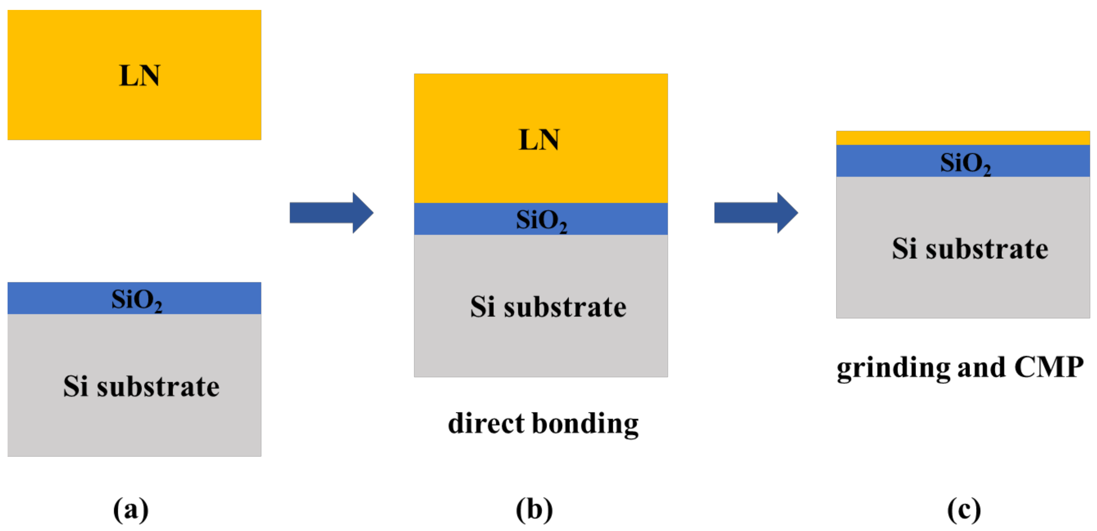
2, and an x-cut LNOI with a thickness of 700 nm was fabricated. The LNOI was annealed at 350 °C (LNOI annealing at 350 °C) or 500 °C (LNOI annealing at 500 °C) to repair lattice damage caused by ion implantation. The process of fabricating LNOI by wafer bonding and grinding (grinded LNOI) is shown in
Figure 1. First, a layer of SiO
2 was grown on an Si substrate by thermal oxidation, and the SiO
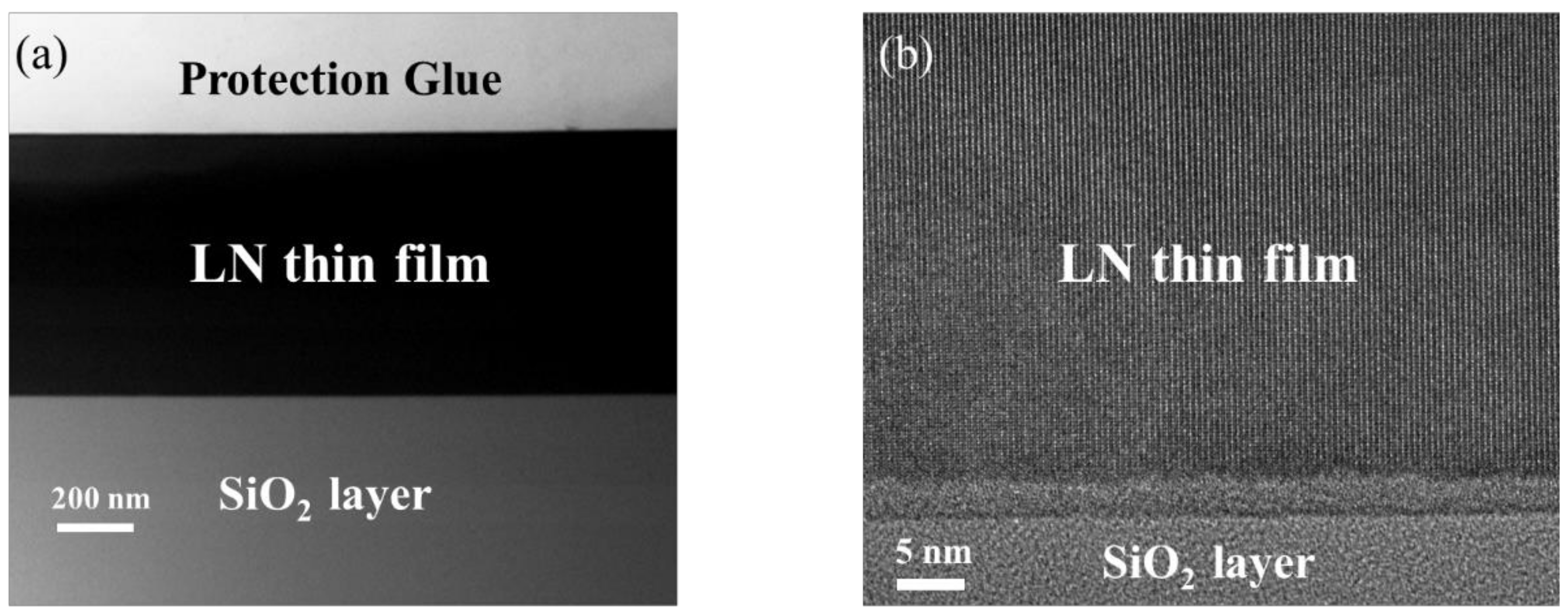
2 was polished to a suitable thickness (2 microns) by chemical mechanical polishing (CMP). Then, an x-cut LN wafer was directly bonded to the Si substrate. Next, the LN crystal was grinded to a suitable thickness and CMP was used to reduce the surface roughness of the thin film to less than 0.5 nm. Finally, an x-cut LNOI with a thickness of 700 nm was fabricated, which could avoid lattice damage caused by the ion implantation process. High-resolution transmission electron microscope (HRTEM) was used to investigate the interface and crystal lattice of the grinded LNOI.
Figure 2a shows a TEM image in which the LNOI structure is clearly seen.
Figure 2b shows a high-magnification TEM image, with a clear film interface between LN and SiO
2 and an ordered lattice arrangement of LN.
HRXRD with Cu K
α1 (λ = 1.54056 Å) as the X-ray radiation source was used to investigate the lattice properties of the LNOI. First, ω, ψ and χ scans were used to find the (110) crystal plane of the LNOI, and then an ω-2θ scan with a step of 0.0012° was used to measure the diffraction peak of the LNOI. Confocal Raman spectroscopy was used to investigate the LNOI as well. A 473 nm laser beam was focused onto the surface of the LN thin film through a 100× objective lens (NA = 0.9), achieving a depth resolution of approximately 320 nm. Raman probing was performed using an 1800 lines/mm grating, achieving a spectral resolution of 0.69 cm
−1/pixel. Multiple electric pulses were used to study the domain polarization inversion of the LNOI [
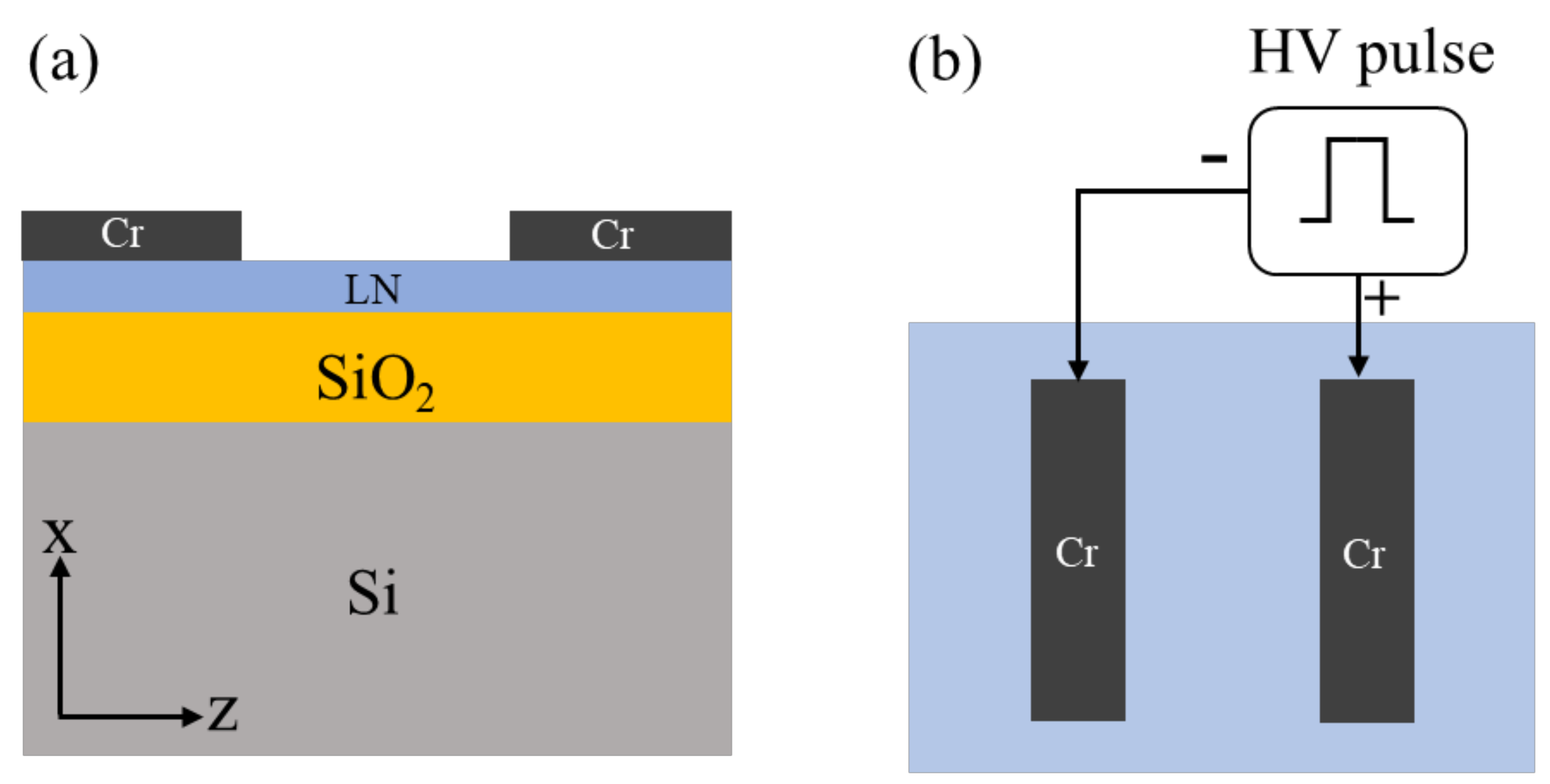
14]. The domain polarization inversion was achieved by applying high voltage pulses to the metal electrode deposited on the LNOI. As shown in
Figure 3a, a 100-nm-thick Cr electrode was deposited on an x-cut LN thin film with a thickness of 700 nm.
Figure 3b shows the scheme of the domain polarization inversion configuration. The pulse period and duty cycle were 0.1 s and 50%, respectively. The number of pulses was 20. The direction of the electric field was along the z axis of the LN thin film. The sample was put in silicone oil to avoid air breakdown caused by the high electric field strength. Piezoresponse force microscopy (PFM) was used to observe the inversion domains.
A waveguide phase modulator was fabricated on the LNOI to measure the E-O coefficient
r33. The LN thin film was x-cut and the TE light traveled along the y axis. The two polished end faces of the waveguide formed a low-finesse Fabry–Perot cavity [
23]. By applying a continuously varying voltage to the electrodes on either side of the waveguide, the output light intensity will oscillate. The relationship between the half-wave voltage length product
VπL and
r33 is expressed as follows [
24,
25]:
where
G and
L are the gap and length of the electrodes, respectively.
λ is the wavelength,
neff is the effective index of the waveguide, and
n is the extraordinary refractive index of LN. The
Γ (overlapping factor) is defined as follows:
where
V is the voltage applied to the electrode,
Eele is the electrostatic field, and
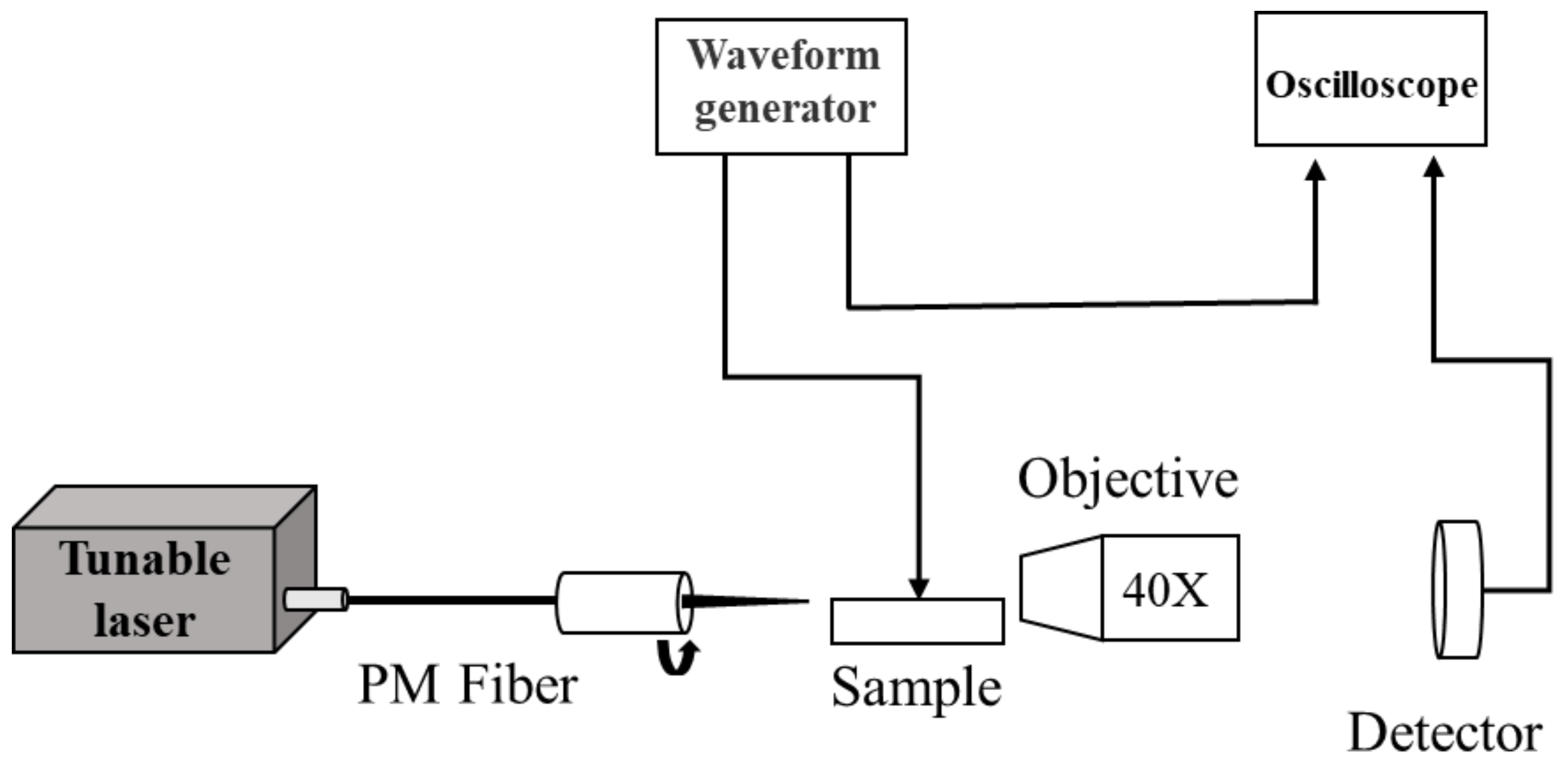
Eopt is the optical field. The measurement setup is shown in
Figure 4. Polarized light with a wavelength of 1550 nm was emitted from a tunable semiconductor laser (Santec TSL-210). The laser beam was coupled into the waveguide by a polarization-maintaining (PM) fiber, and the output light was collected by a 40×/0.65 objective lens and displayed in an oscilloscope by an InGaAs detector. The electrical signal from the waveform generator was applied to the electrode to modulate the light signal in the waveguide. The electrostatic field (
Eele) and optical field (
Eopt) were simulated by Charge Solutions and Mode Solutions, respectively.
3. Results and Discussion
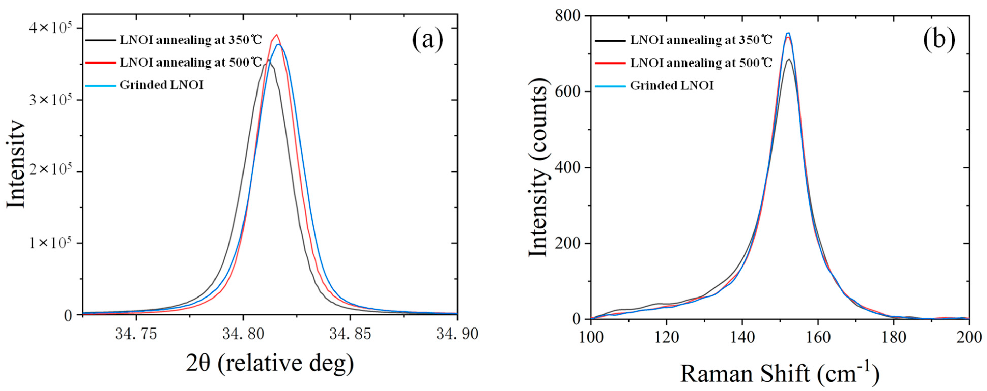
Figure 5a shows the diffraction peaks of the (110) crystal planes of the LNOI as measured by HRXRD. The black line from LNOI annealing at 350 °C had a diffraction peak of 34.809° and a FWHM of 0.026°. The red line from LNOI annealing at 500 °C had a diffraction peak of 34.815° and a FWHM of 0.026°. The blue line from grinded LNOI had a diffraction peak of 34.817° and a FWHM of 0.027°. The FWHMs were small, showing that the LNOI was mono-crystalline with an ordered crystal-lattice arrangement. The FWHM of LNOIs did not show significant differences. To study the lattice structure after undergoing the ion implantation process,
Figure 5b shows the polarized Raman spectra of the LNOI at 153 cm
−1 with an X(YZ)X scattering configuration. The blue line from the grinded LNOI had a FWHM of 9.41 cm
−1. The black line from the LNOI annealing at 350 °C had a FWHM of 10.75 cm
−1, which was broadened, potentially due to the disorder of the crystal lattice. The red line from the LNOI annealing at 500 °C had a FWHM of 9.41 cm
−1. The FWHM of LNOI annealing at 500 °C was consistent with that of grinded LNOI, revealing that the crystal lattice of the LN thin film was well recovered without causing an expansion of the frequency range of the lattice vibration.
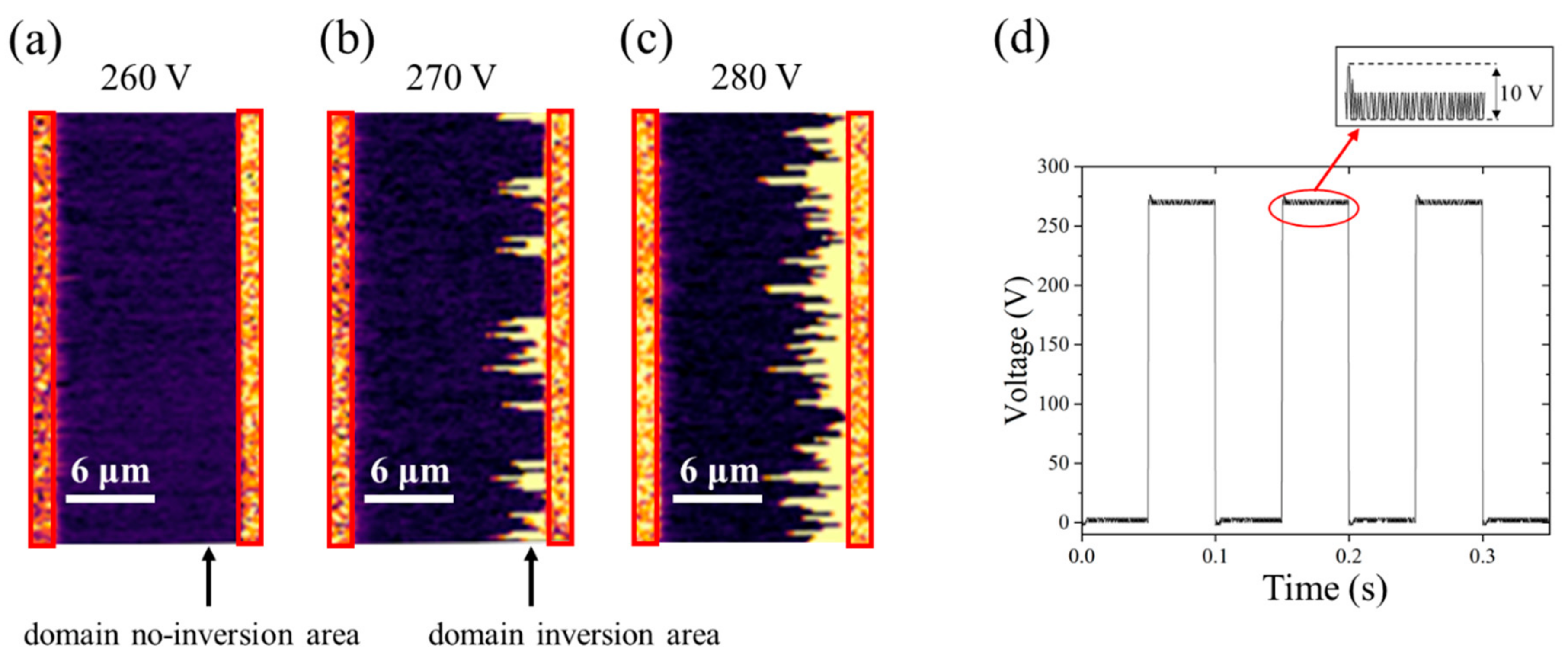
The ion implantation process affects the domain inversion voltage of the LNOI.
Figure 6 shows the PFM images of domain inversion of LNOI annealing at 350 °C. The areas inside the red frame are the electrodes. The gap between the metal electrodes was 11.2 μm. As shown in
Figure 6a–c, when the voltage was 260 V, there was no domain inversion. When the pulse voltage increased to 270 V, domain inversion was found. Upon increasing the voltage to 280 V, the domain inversion area increased.
Figure 6d shows the electrical pulse waveform when the voltage was 270 V. The voltage fluctuation error was 10 V. Therefore, the domain inversion voltage of LNOI annealing at 350 °C was 270 ± 10 V (24.1 ± 0.9 kV/mm). As shown in
Table 1, the same method was used to measure the domain inversion voltages of LNOI annealing at 500 °C and grinded LNOI, which were 20.7 ± 0.9 and 20.4 ± 0.9 kV/mm, respectively, close to that of LN bulk material (~21 kV/mm). The domain inversion voltage of LNOI annealed at 350 °C is higher than that of LNOI annealed at 500 °C. A possible explanation is that the LN crystal-lattice disorder caused by ion implantation increased the domain inversion voltage. With the increase in annealing temperature, the LN crystal lattice damage was repaired, and the domain inversion voltage decreased.
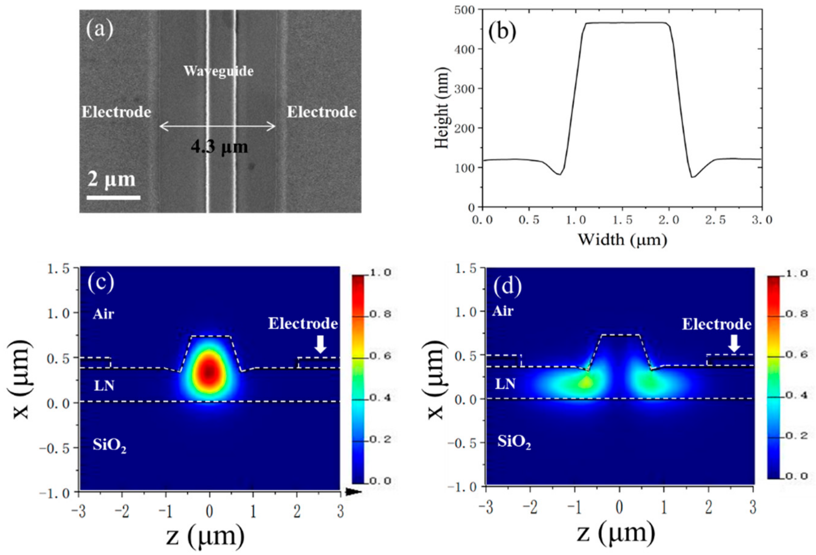
Figure 7a shows a scanning electron microscope (SEM) image of the phase modulator in grinded LNOI. The gap and length of the electrodes were 4.3 μm and 5 mm, respectively.
Figure 7b shows an atomic force microscope (AFM) image of the LNOI waveguide cross-section. The rib had a top width of 0.9 µm and a bottom width of 1.4 µm. The LN etch depth was 350 nm, leaving a 370 nm slab (measured by the white light interferometry method).
Figure 7c,d show the profiles of the TE
00 and TE
10 mode at 1550 nm. When the gap of the electrodes was 4.3 μm, the transmission losses of the TE
00 and TE
10 mode were simulated to be 0.5 and 520 dB/cm, respectively. Owing to the high transmission loss of the TE
10 mode, the waveguide could be considered to be single-mode transmission.
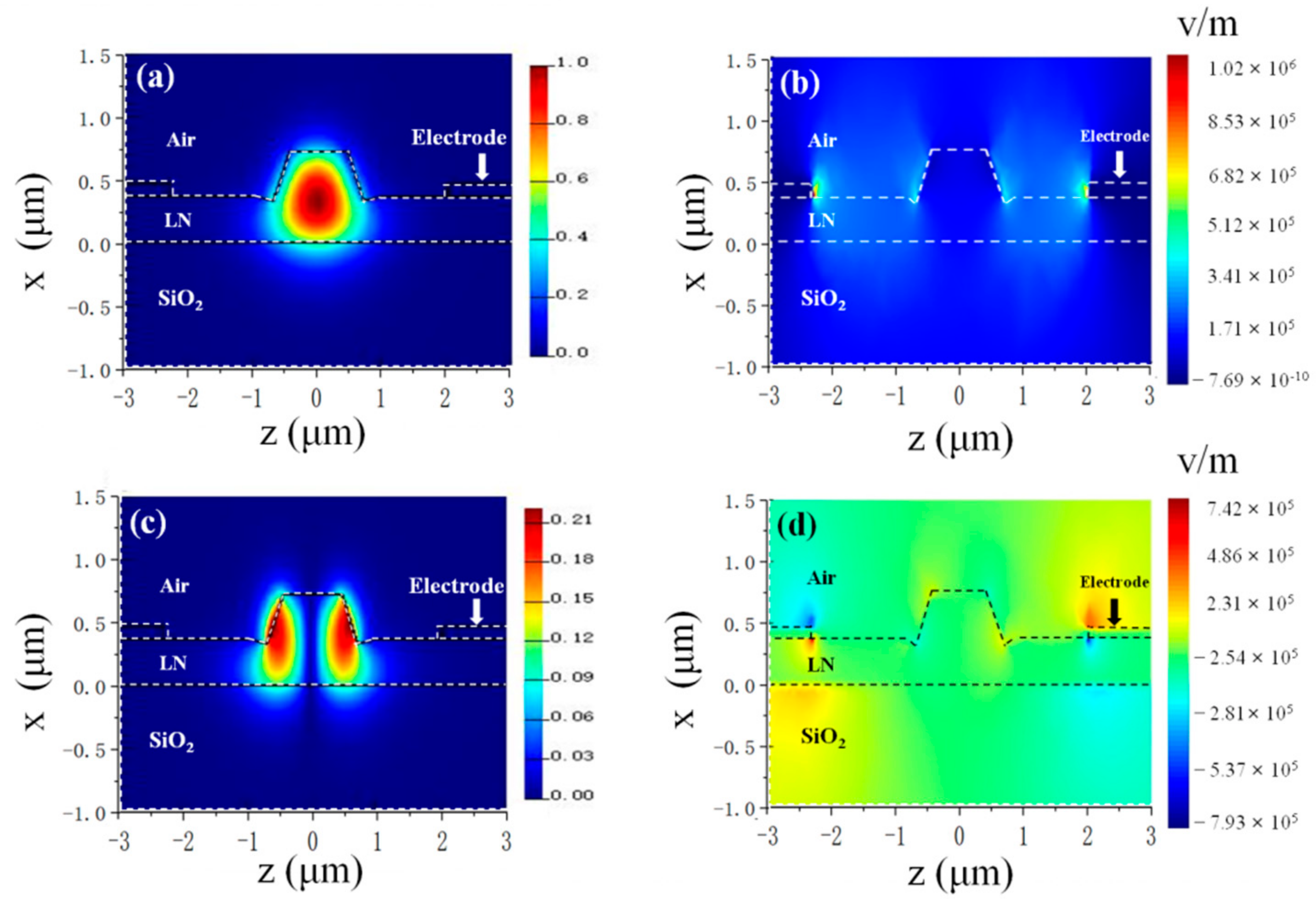
Figure 8a,c show the electric fields E
z and E
x, respectively, of the TE
00 mode.
Figure 8b,d show the electric fields E
z and E
x, respectively, of the electrostatic field after a voltage of 1 V was applied to the electrodes. Because the overlapping factors Γ of the E
x of the TE
00 mode and the E
x of the electrostatic field were almost 0, their contribution to the phase change of the TE
00 mode can be ignored. The overlapping factors Γ of the E
z of the TE
00 mode and the E
z of the electrostatic field were 0.53.
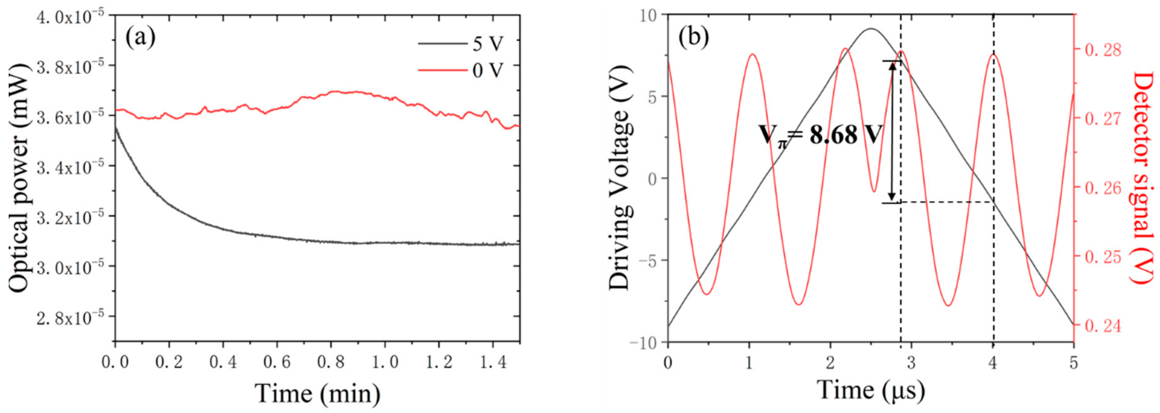
Figure 9a shows the variation of output light power with time after applying volt-ages of 5 and 0 V on the electrodes. When the voltage was 0 V, the output light power was stable with time; when the voltage was 5 V, the output light power varied significantly with time. The light power variation was related to the DC bias drift, which resulted from the flow and redistribution of electrical charge in the LN region under DC voltage [
26]. This phenomenon would cause uncertainties in the measurement of V
π. Triangular waves (200 kHz with an amplitude of 18 V) were used to minimize the influence of the DC bias drift.
Figure 9b shows the measured light transmission at 1550 nm. The red and black lines represent the triangular wave electrical and optical signals, respectively, indicating a V
π of 8.68 V. The uncertainty of the E-O coefficient mainly results from two aspects. One was the overlapping factor calculation error caused by the uneven morphologies of the waveguide and electrodes. The other was Vπ measurement error. The uncertainty of the E-O coefficient was estimated to be within 3%. The E-O coefficient of ground LNOI was 27.3 ± 0.4 pm/V, which was close to that of LN bulk materials (28.6 pm/V [
27]). The stress at the interface between LN thin film and SiO
2 might cause the E-O coefficient of LNOI to be smaller than that of LN bulk material [
28]. As shown in
Table 2, using the same method, the E-O coefficient of LNOI annealing at 350 °C was 26.1 ± 0.4 pm/V, which was lower than grinded LNOI. This might be due to lattice damage caused by ion implantation.
4. Conclusions
In conclusion, the lattice properties, domain inversion voltage, and E-O coefficient of LNOIs were studied. For grinded LNOI, the FWHM of the (110) plane of HRXRD was 0.027°, and the FWHM of Raman spectrum at 153 cm−1 was 9.41 cm−1, revealing a regular lattice arrangement; the domain inversion voltage was 20.4 ± 0.9 kV/mm, which was close to that of bulk material. The E-O coefficient of LNOI was 27.3 ± 0.4 pm/V, which was close to that of bulk material. After annealing at high temperature, the LNOI fabricated by ion implantation and wafer bonding exhibited properties similar to those of LNOI fabricated by wafer bonding and grinding, which indicated that both methods could produce high-quality LNOIs.


