1. Introduction
To the best of our knowledge, the noble metallic element at the nanoscale introduces extraordinary optical characteristics, the localized surface plasmon resonance (LSPR) [
1]. This LSPR happens when electrons in the nanoparticles are stimulated by a particular wavelength of light that falls on the metal nanoparticles. LSPR properties rely on the form, size, and placement of nanostructures [
2]. In particular, the spectral extinction is contingent on the refractive index of the surrounding medium. Some small changes in the local dielectric environment, such as molecular adsorption on the nanostructure surface, affect the spectral extinction characteristics [
3]. The few behavioral changes are demonstrated as changes in the number of scattered, transmitted, and absorbed light at dissimilar wavelengths and can be analyzed with high spectral resolution in an ordinary optical transmission or reflection configuration. Moreover, metallic nanostructures have been developed for plasmonic biosensors. The nanofabrication of novel metallic nanostructures, for instance, nano-ring, suggests its applications for a plasmonic biosensor [
4,
5,
6,
7]. Gold micro-/nano-ring structures are expected to provide basic implemented feasible structures for plasmonic biosensing with excellent detection performance [
8]. Due to the need for biosensing applications, an efficient nanofabrication method to produce the ordered gold micro-rings with tunable LSPR properties is demanded.
Novel metal nanostructures are generally produced via conventional nanofabrication approaches, for instance, extreme UV Lithography [
9,
10], Focus Gallium Ion Beam Milling [
11,
12], and E-Beam Exposure Lithography [
13,
14]. While these techniques can produce nanostructures with a well-controlled size, shape, and alignment, they need costly facilities, stringent processes, and cannot address the problem of low throughput. Nanoimprinting with Thermal/UV Lithography (NIL) is a preferred conventional approach, and it shows the advantage of high resolution. However, the nanopattern mold necessary in the NIL process is usually created via conventional lithography techniques. Hence, NIL cannot overcome the disadvantages of conventional lithography processes [
15,
16,
17,
18,
19,
20]. Another technique for the nanofabrication of metallic nanoarrays is the annealing technique of a metal layer on a glass plate [
21,
22]. An annealing process enables us to produce metal nanopatterns with an easy annealing technique. Nevertheless, it is hard to control the size and alignment of the metal nanoarrays.
To address these problems and supplement the limitations of the current fabrication methods, the authors propose the efficient nanofabrication process to fabricate the gold micro-ring arrays on a glass plate by a combination of soft stamping and the thermal uplifting method. The objective of this study is to verify the solution possible with the combination of fabrication techniques and demonstrate its capability to achieve gold micro-rings with a huge pattern and low nanofabrication costs.
2. Materials and Methodologies
2.1. Plastic Film Mold
A thermoformable biaxially oriented polyethylene terephthalate film (Polyplex Thailand, BOPET, SH140) of 50 µm thickness was utilized to be a soft stamping mold. The hot embossing process is employed for the fabrication of a film mold. The nanohole pattern on the master mold on a silicon wafer was transferred onto a BOPET film via the hot stamping process.
Figure 1 demonstrates the atomic force microscopy figures and a line profile of the height of a BOPET mold.
Figure 1a represents an image of micropillar patterns, and
Figure 1b is the line of height profile of the pillar patterns. The result shows that the mean diameter of the pillars was about 2.1 µm, and the mean peak was 900 nm.
Figure 1c was a 3-dimensional topography of micropillar structures. The BOPET film mold was utilized for the soft stamping process. Subsequently, the word “microdot” was utilized to express a chemical templated by the micropillar patterns of a BOPET stamp.
2.2. Experiment Procedure of Soft Stamping Processes
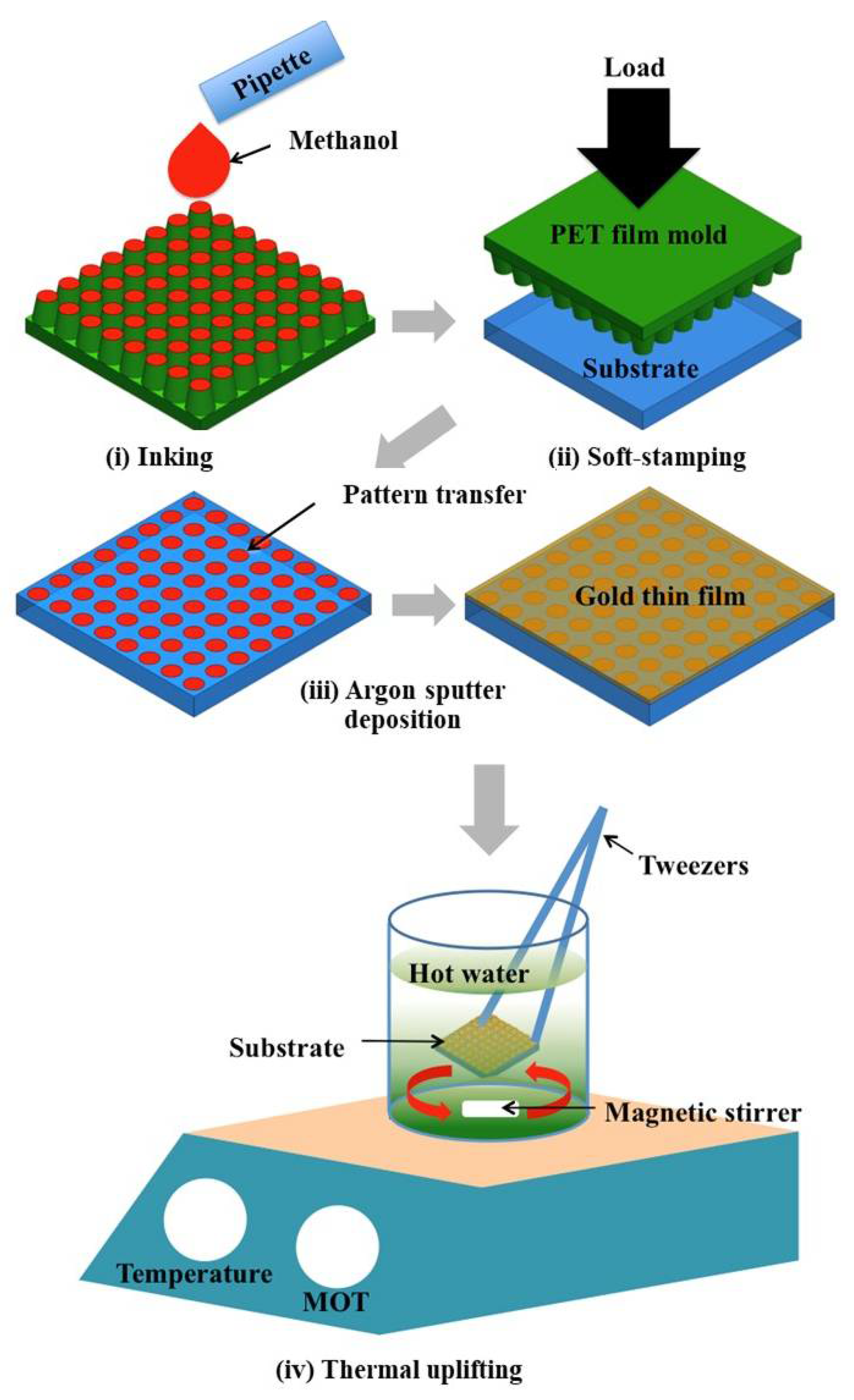
Figure 2 shows the microfabrication processes of gold micro-ring structures on a quart glass plate for this study. A quartz glass plate was 1 mm in thickness, 12 × 12 mm
2, and was washed in an acetone bath with an ultrasonic cleaner machine for 10 min. Then, a glass plate was dried at room temperature. A dried glass plate was etched by etching with Argon for 1 min to reduce the impurities of the glass plate. (i) The methanol was dropped onto a BOPET mold. (ii) The BOPET mold with the methanol was manually impressed onto an etched surface of a glass plate. (iii) Then, a stamped glass plate was coated with a gold layer in the sputtering machine. The spatter gas was Argon, with a pressure of about 15 Pa. The vertical gap between a glass plate and a gold target was about 35 mm. The voltage was provided at 0.8 kV, and the coating current was maintained at 10 mA throughout the coating operation. The thickness of a gold thin film was controlled by adjusting the coating time. (iv) A micro-ring aggregation process uses a thermal uplifting technique inspired by the vibrating hot bath processes. A glass plate was dipped into a hot water bath. The magnetic stirrer with a heating plate was utilized to control the temperature of water to 100 degrees Celsius. The protuberance of the gold micro-ring patterns on a glass plate was analyzed with an Atomic Force Microscope, CoreAFM, Nanosurf.
3. Results
3.1. The Soft Stamping Technique with Gold Thin Film Sputtering Process
Figure 3a demonstrates a topography figure using the atomic force microscope, and
Figure 3b shows the peak profiles of a gold layer coated onto a methanol templated glass plate. The gold layer was about 30 nm in thickness. It was revealed that the microdots had appeared on a gold thin layer.
Figure 3c illustrates a 3D atomic force microscope image topography. It was revealed that a peak of gold layer on the methanol stamped area was raised up. The mean diameter of the microdots was 1000 nm, with a mean peak of 140 nm.
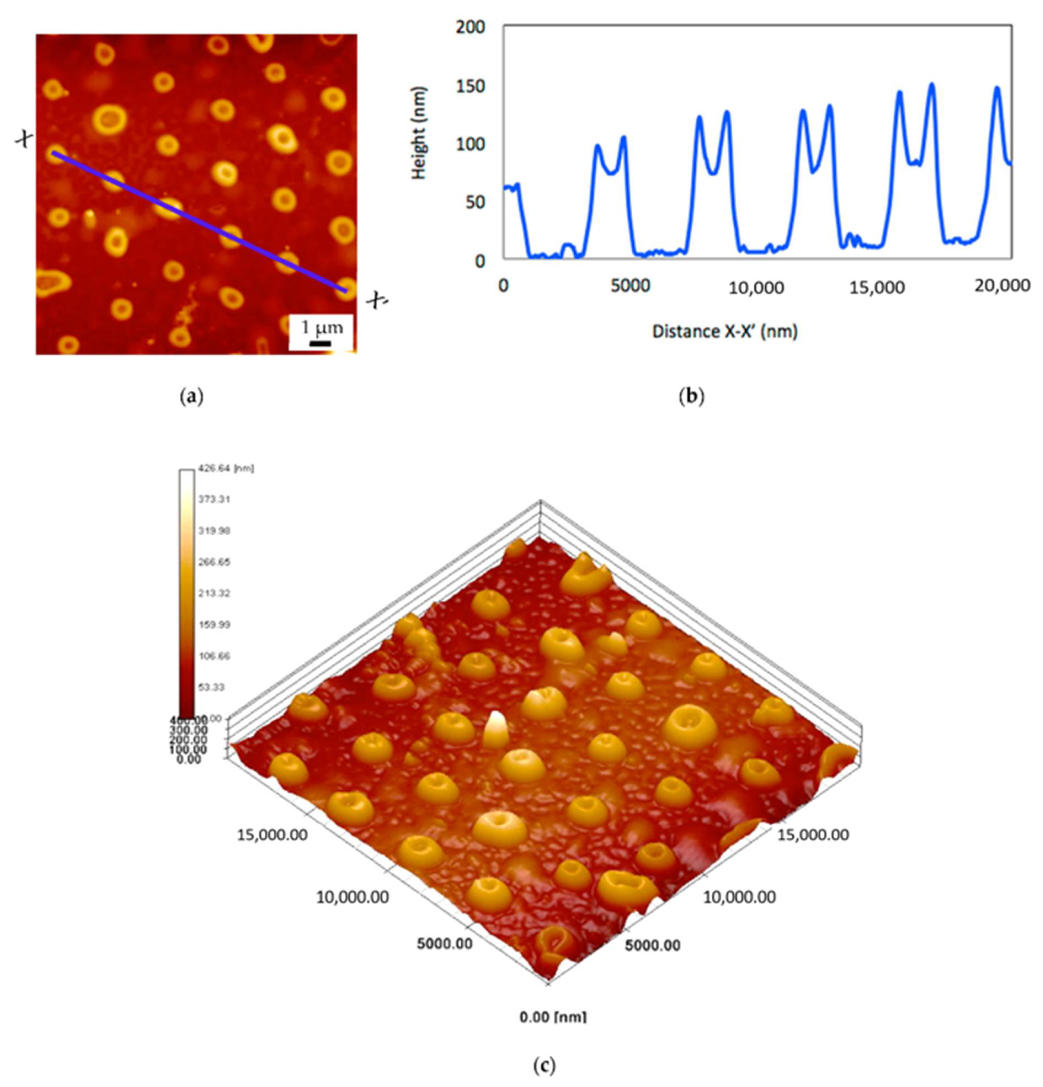
3.2. The Thermal Uplifting Process
Figure 4a demonstrates a topography figure using the atomic force microscope,
Figure 4b shows the peaks, and
Figure 4c demonstrates a 3D atomic force microscopy figure topography of the gold micro-rings aggregated on a glass plate after a thermal uplifting technique in a hot water bath of 100 °C for 10 min. The result showed that the mean diameter of the stamped template was broadened to 1100 nm. The difference between the height of the edge and the center of the gold micro-ring array was 50 nm. It was also revealed that the gold thin films had agglomerated into the micro-ring structures on a methanol stamped glass plate.
3.3. The Spectral Absorbance Properties
The optical characteristics of the gold layer on a glass plate were assessed via extinction spectrum.
Figure 5 demonstrates the spectral absorbance of the gold arrays originating on a glass plate with the different structures. Consecutively, (i) a blue line illustrates the absorbance spectrum of the gold micro-rings on a glass plate. A peak of spectral absorbance was discovered at a wavelength of 500 nm. (ii) A red line shows the absorbance spectra of a gold microdots on a methanol stamped substrate. The peak of spectral absorbance was discovered at a wavelength of 560 nm, and the height of the peak is lower than the absorbance of gold micro-rings. (iii) A black line shows the absorbance spectra of a bare gold layer on a glass plate. The absorbance graph is relatively flat and has no peaks. It was revealed that the agglomeration and alignment of the micro-ring arrays are the important variables for the spectral absorbance properties. It was also revealed that the good uniformity of micro-ring structures led to higher improvement, while an exposed gold layer caused a reduction in the height and an expansion of the spectral absorbance. It is conceivable that the enhanced spectral absorbance can be controlled by the gold micro-ring structures on a quartz glass plate [
23,
24].
4. Discussion
It has been established that an absorption behavior is a surface-based physicochemical process that creates a layer of an adsorbate on the surface of the glass plate. According to this study, a quartz glass plate was etched using an Argon sputtering machine. The ions of argon gas are more efficient in breaking off pieces of a glass plate. An electrical discharge is generated in a vacuum chamber by employing a voltage on a glass plate. The ions of argon are pulled onto a plate and therefore onto a glass plate with electron volts power the same as the setting voltage of 0.8 kV. Then, the argon ions are generated by creating an arc that travels across the surface of the target. The arc strikes lead to the ejection of H
2O and SiO
2 atoms onto a glass plate. Since an adhering between H
2O and a glass plate atom is cracked by the Argon gas etching, glass atoms are stimulated, then the surface energy on a glass plate is raised. It is revealed that a glass plate’s surface energy is increased by the argon ion spatter etching technique.
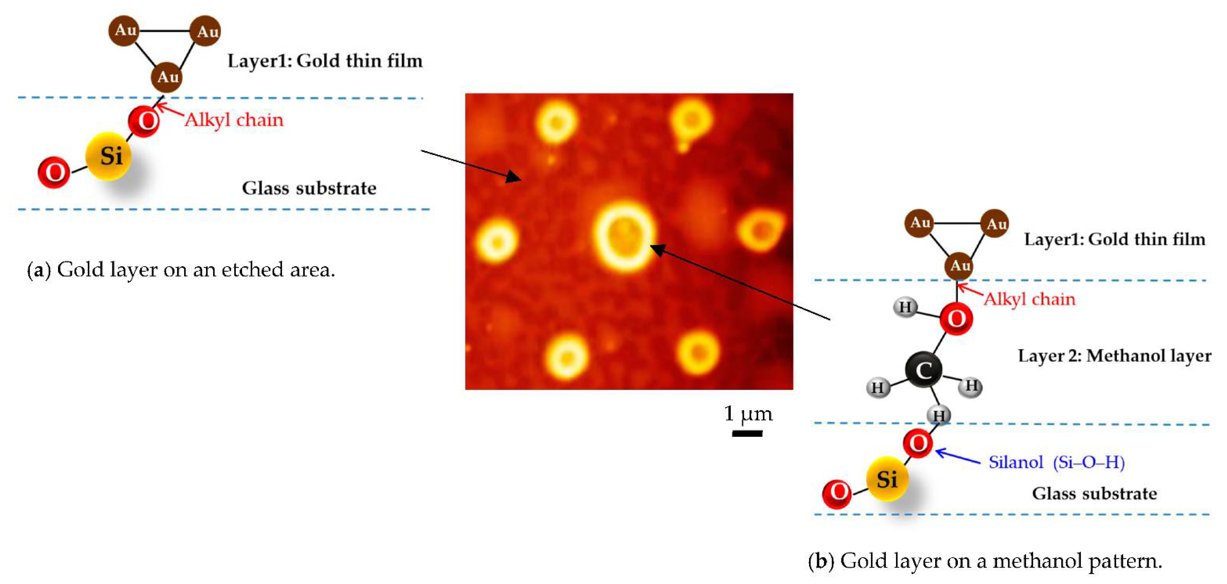
Figure 6a shows the layer of gold directly adhered to an etched area on a substrate. It is confirmed that throughout a thermal uplifting process, the adhering strength between a glass plate and a gold layer is higher than the uplifting force of vibrating hot bath processes. Therefore, a gold thin layer in the etched area perfectly adheres to a glass plate.
However, the surface energy between a gold layer and the etched glass is the most significant parameter for the aggregation of micro-ring structures.
Figure 6b shows a layer of methanol that was attached to a glass substrate. Methanol is absorbed by this mechanism on a porous glass plate [
25]. The adhering of SiO
2 with a methanol carbonyl group on a glass atom affects the glass plate surface energy. It is confirmed that a glass plate’s surface energy is decreased by a methanol layer between a gold layer and a glass plate. The adhesion strength between a gold layer and a glass plate surface is decreased. Then, a gold layer on a methanol-stamped template is uplifted as the micro-ring arrays via the thermal uplifting technique. It was preferable to cause a large difference in the surface energy between an etched area and the methanol templated area to enhance the arrangement of the gold micro-ring aggregation process.
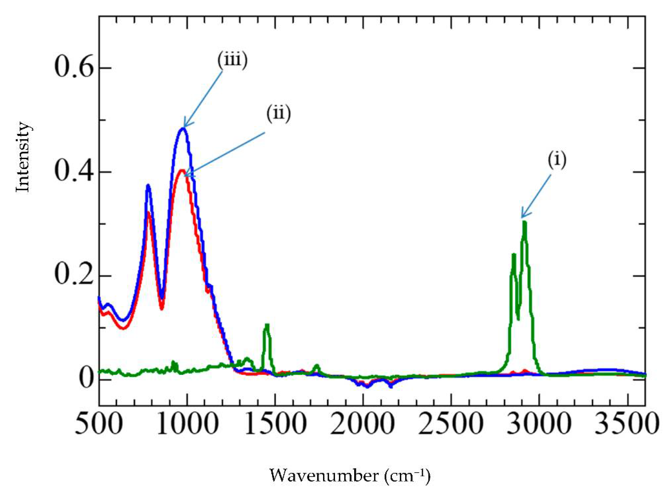
Fourier transform infrared spectroscopy (FTIR Spectroscopy, Thermo Scientific, Thailand, Nicolet iS5) was used to observe the chemical properties of material and tools in the soft stamping process.
Figure 7 illustrates the FTIR spectra. (i) The green curve shows the spectrum of a BOPET film mold. The spectrum of the BOPET film has peaks between 2800 and 3000 cm
−1. (ii) The red curve illustrates the spectra of the dried methanol on a quartz glass plate. It has a sharp peak at 1000 cm
−1. (iii) The blue curve shows the spectrum of a quartz glass specimen that was stamped with a BOPET film mold, which was spotted with methanol. It has a sharp peak at 1000 cm
−1 and is higher than (ii). Results show that the difference between (ii) and (iii) is not very large. However, the absorbance spectra of (i) are very different from those of (ii) and (iii). It was also confirmed that the BOPET molecules were not transferred to the quartz glass via the chemical stamping process. Therefore, the methanol molecule did not dissolve the BOPET film mold and did not affect the pattern transfer on the substrate. Moreover, this study does not utilize stringency in the processes.
To overcome the issues of low productivity associated with the top-down fabrication method, bottom-up fabrication techniques have recently been given attention as an alternative manufacturing strategy. This method involves fabrication techniques via self-organization methods. Nanosphere lithography (NSL) is a widespread bottom-up fabrication technique to pattern solid surfaces with sub-micrometer and nanometer-scale features. NSL is a simple and very high throughput system. However, the limitation is the geometrical constraint of the nanosphere template. Another approach is the porous anodic alumina technique. This technique shows the advantage that it can be used to fabricate large-area nanostructures with a very high aspect ratio. However, the limitation is the geometrical constraint of the template. Another self-organization is the thermal dewetting method. This process offers the advantage of being a simple fabrication process. However, thermal dewetting suffers from the disadvantage of random distribution of the dot dimensions. In conclusion, bottom-up methods are often utilized to fabricate nanostructures with high throughput. However, it is difficult to control the size and distribution of nanostructures by self-assembly methods.
In this study, the advantage of the soft stamping technique of the BOPET mold is that it can be reused as a stamped mold. The micropillar pattern was fabricated onto a BOPET film via the embossing method. The BOPET mold can be very low-cost and easy to utilize. The A4 dimension of the marketable BOPET was produced to form a 10 × 10 mm
2 for about 300 copies. Most significantly, a BOPET mold was used as a soft stamping tool to produce the metallic micro-ring arrays on a glass plate without lithography equipment. The comparison between each micro/nanofabrication method is summarized as shown in
Table 1.
5. Conclusions
In this study, an efficient microfabrication method of gold micro-ring structures using soft stamping with a thermal uplifting technique was proposed. A BOPET mold was utilized as a soft stamping mold to make the chemical templates on a quartz glass plate. The thermal uplifting process of a gold layer on a glass plate was studied experimentally. The proposed technique is effective in producing gold micro-ring arrays on a glass plate. A BOPET mold is used for methanol stamped on an etched glass plate. The round shape templates of methanol can be adhered to and dried on a glass plate. Then, a gold layer was coated onto a stamped glass plate. The thermal uplifting technique of the vibrating hot bath process was used for the aggregation of gold micro-ring structures.
It was confirmed that inhibition of adhering between the gold layer and a glass plate via a methanol soft stamping process affected the thermal uplifting of the gold layer. Due to an Argon etching, the surface energy on a glass plate was raised, and it caused strong adhesion between a gold cluster layer and a glass plate. At the same time, the surface energy of the methanol stamped region was decreased by a methanol atom templated by a BOPET mold, and a gold layer in this region was self-uplifted by the vibrating hot bath processes. It was also revealed that the preference of this proposed method is that it does not require a costly machine other than a sputtering machine.
The spectral absorbance of the micro-ring arrays on a glass plate shows a peak in the visible light region. The spectral absorbance height intensity was raised when the gold micro-rings were arranged along with the templated thermal uplifting. It was revealed that a multiformity in the spectral absorbance characteristic has intimately corresponded to the aggregation of gold micro-ring structures on a quart glass plate.
Author Contributions
Conceptualization, P.P., J.P. and I.N.; methodology, P.P.; investigation, P.P. and I.N.; resources, P.P. and J.P.; writing—original draft preparation, P.P.; writing—review and editing, P.P.; visualization, P.P.; supervision, P.P.; project administration, P.P.; funding acquisition; P.P., J.P. and I.N. All authors have read and agreed to the published version of the manuscript.
Funding
The authors gratefully acknowledge the funding by the Thailand Science Research and Innovation Fund and the University of Phayao, Thailand (Grant No. FF65-RIM086). This work was supported by the National Research Council of Thailand.
Institutional Review Board Statement
Not applicable.
Informed Consent Statement
Not applicable.
Acknowledgments
This research project was supported by the Thailand Science Research and Innovation Fund and the University of Phayao, Thailand (Grant No. FF65-RIM086).
Conflicts of Interest
The authors declare no conflict of interest.
References
- Taerin, C.; Seung, Y.L.; Eui, Y.S.; Honggu, C.; Byoungho, L. Plasmonic nanostructures for nano-scale bio-sensing. Sensors 2011, 11, 10907–10929. [Google Scholar]
- Guo, Y.Y.; Qing, L.L.; Zong, Y.Z. Studied localized surface plasmon resonance effects of Au nanoparticles on TiO2 by FDTD simulations. Catalysts 2018, 8, 236. [Google Scholar]
- Attila, B. Maximizing the surface sensitivity of LSPR biosensors through plasmon coupling—Interparticle gap optimization for dimers using computational simulations. Biosensors 2021, 11, 527. [Google Scholar]
- Hai, L.; Cong, C.; Yanzeng, Z.; Bingbing, B.; Shoufeng, T. A high-sensitivity methane sensor with localized surface plasmon resonance behavior in an improved hexagonal gold nanoring array. Sensors 2019, 19, 4803. [Google Scholar]
- Jen, H.H.; Yulu, H.; Jian, H.Y.; Po, H.T.; Wei, H.H.; Meng, C.L.; Yu, H.T.; Cheng, J.C.; Cheng, C.H.; Yean, W.K.; et al. Enhancements of cancer cell damage efficiencies in photothermal and photodynamic processes through cell perforation and preheating with surface plasmon resonance of gold nanoring. Molecules 2018, 23, 3157. [Google Scholar]
- Zhang, L.; Zhu, T.; Yang, C.; Jang, H.Y.; Jang, H.J.; Liu, L.; Park, S. Synthesis of monolayer gold nanorings sandwich film and its higher surface-enhanced raman scattering intensity. Nanomaterials 2020, 10, 519. [Google Scholar] [CrossRef] [Green Version]
- Chou Chao, C.T.; Chou Chau, Y.F.; Huang, H.J.; Kumara, N.T.; Kooh, M.R.; Lim, C.M.; Chiang, H.P. Highly sensitive and tunable plasmonic sensor based on a nanoring resonator with silver nanorods. Nanomaterials 2020, 10, 1399. [Google Scholar] [CrossRef]
- SS dos Santos, P.; MMM de Almeida, J.; Pastoriza-Santos, I.; CC Coelho, L. Advances in plasmonic sensing at the NIR—A review. Sensors 2021, 21, 2111. [Google Scholar] [CrossRef]
- Anna, L.G.; Andreas, B.; Alexander, N.-M.; Reiner, D. Design strategy for nanostructured arrays of metallodielectric cuboids to systematically tune the optical response and eliminate spurious bulk effects in plasmonic biosensors. Bioengineering 2022, 9, 63. [Google Scholar]
- Theodore, M.; Panagiotis, A. High sensitivity resists for EUV lithography: A review of material design strategies and performance results. Nanomaterials 2020, 10, 1593. [Google Scholar]
- Mariachiara, M.; Marco, E.; Adriana, P.; Massimo, C.; Vittorianna, T. Focused ion beam processing for 3D chiral photonics nanostructures. Micromachines 2021, 12, 6. [Google Scholar]
- Frances, I.A. Branched high aspect ratio nanostructures fabricated by focused helium ion beam induced deposition of an insulator. Micromachines 2021, 12, 232. [Google Scholar]
- Luisa, B.; Jakub, J.; Katarzyna, M.; Iwona, B.S.; Patrik, H.; Ivo, U. Room temperature direct electron beam lithography in a condensed copper carboxylate. Micromachines 2021, 12, 580. [Google Scholar]
- Mikhail, Y.F.; Lyudmila, V.F.; Artem, M.C.; Pavel, N.D.; Valery, P.K. Fabrication of superconducting Nb–AlN–NbN tunnel junctions using electron-beam lithography. Electronics 2021, 10, 2944. [Google Scholar]
- Michael, M.; Stephan, R.; Dieter, N.; Amiya, M.; Maria, R.B.; Philipp, T.; Sonja, K.; Heinz, D.W.; Adrian, P.; Daniel, F. Nanoimprint replication of biomimetic, multilevel undercut nanostructures. Nanomaterials 2021, 11, 1051. [Google Scholar]
- Christine, T.; Martin, E. UV nanoimprint lithography: Geometrical impact on filling properties of nanoscale patterns. Nanomaterials 2021, 11, 822. [Google Scholar]
- Vaclav, P.; Vaclav, C.; Pavel, K.; Milos, N.; Sonja, K.; Michael, M. Optical polymer waveguides fabricated by roll-to-plate nanoimprinting technique. Nanomaterials 2021, 11, 724. [Google Scholar]
- Michael, M. Nanoimprinting of biomimetic nanostructures. Nanomanufacturing 2022, 2, 17–40. [Google Scholar]
- Janek, B.; Danbi, Y.; Markus, K.; Martina, G. Two-dimensional nanograting fabrication by multistep nanoimprint lithography and ion beam etching. Nanomanufacturing 2021, 1, 39–48. [Google Scholar]
- Stefan, S.; Michael, J.H.; Tina, M.; Michael, M.; Astrit, S.; Hubert, B.; Martin, B.; Theodoros, D.; Barbara, S.; Joerg, S. Multifunctional nanostructures and nanopocket particles fabricated by nanoimprint lithography. Nanomaterials 2019, 9, 1790. [Google Scholar]
- Potejana, P.; Sethavut, D. Gold nanoisland agglomeration upon the substrate assisted chemical etching based on thermal annealing process. Crystals 2020, 10, 533. [Google Scholar] [CrossRef]
- Gabriele, B.; Federica, C.; Matteo, C.; Marco, C.; Paola, R.; Paola, T. Effect of the substrate crystallinity on morphological and magnetic properties of Fe70Pd30 nanoparticles obtained by the solid-state dewetting. Sensors 2021, 21, 7420. [Google Scholar]
- Potejana, P. A study on fabrication process of gold microdisk arrays by the direct imprinting method using a PET film mold. Crystals 2021, 11, 1452. [Google Scholar] [CrossRef]
- Victor, I.; Anna, L.; Oxana, R.; Andrei, K.; Denis, K.; Arseniy, A.; Arina, G.; Alexey, E.; Victor, N. Aerosol dry printing for SERS and photoluminescence-active gold nanostructures preparation for detection of traces in dye mixtures. Nanomaterials 2022, 12, 448. [Google Scholar]
- Masashi, M.; Kazue, K. Macrocluster formation of alcohol on silica surface in cyclohexane: Analysis of interfacial energy between adsorption layer and bulk solution. J. Surf. Sci. Nanotech. 2006, 4, 244–248. [Google Scholar]
| Publisher’s Note: MDPI stays neutral with regard to jurisdictional claims in published maps and institutional affiliations. |
© 2022 by the authors. Licensee MDPI, Basel, Switzerland. This article is an open access article distributed under the terms and conditions of the Creative Commons Attribution (CC BY) license (https://creativecommons.org/licenses/by/4.0/).


