Abstract
This paper presents a recent study on the synthesis of AlN nanowires. AlN nanowires were successfully prepared on sapphire substrate by the Al-Sn flux method. The obtained nanowires were hundreds of nanometers in diameter and tens of microns in length. The results of transmission electron microscopy (TEM) show that the growth direction of AlN nanowires was perpendicular to the C axis. The photoluminescence (PL) spectrum of AlN nanowires shows a broad peak, which is ascribed to the defect levels in the AlN bandgap. This work provides a novel method for growing AlN nanowires, which offers a potential material for the application of photoelectron devices.
1. Introduction
As one of the wide-bandgap semiconductor materials, AlN has excellent performance. First of all, it is an important UV luminescent material, with a direct bandgap of 6.2 eV [1]. Secondly, AlN has the characteristics of high thermal conductivity and exceedingly good electronic properties, which makes it an excellent material for high-power electronic devices [2,3]. Moreover, AlN along the C-axis has been used in surface acoustic wave devices due to its good piezoelectric properties [4]. In addition, the lattice constants and thermal expansion coefficient of an AlN crystal are similar to those of a GaN crystal, which makes the AlN crystal suitable as a substrate material for epitaxial growth of the GaN crystal [5].
Compared with AlN crystals, AlN nanowires are potential materials for electronic and photoelectronic applications due to their high specific surface area and unique quantum confinement effects [6]. Therefore, the synthesis and properties of the AlN nanowires have attracted much attention. At present, AlN nanowires have been successfully synthesized by many methods, such as the Al-N direct synthesis method [7], direct sublimation method [8], chemical gas reaction method, and arc discharge method, etc. For example, Zhang et al. [9] successfully synthesized AlN nanowires by a chemical gas reaction method using Al powders as precursors and AlCl3 as an additive. Shen et al. [10] found that abundant AlN nanowires could be obtained by the direct current arc discharge method in five minutes. However, due to the complexity of the arc discharge process itself or the severe impurities from the precursors, the purity of the nanowires obtained is difficult to control.
In this paper, AlN nanowires were successfully obtained using an Al-Sn flux method. N2 was used as the nitrogen source to avoid the possible pollution of NH3. In addition, the vapor pressure of Sn was low, which did not cause great pollution of the product. The synthesized nanowires were characterized and the optical properties were measured. The growth mechanism of AlN nanowires was discussed at length.
2. Materials and Methods
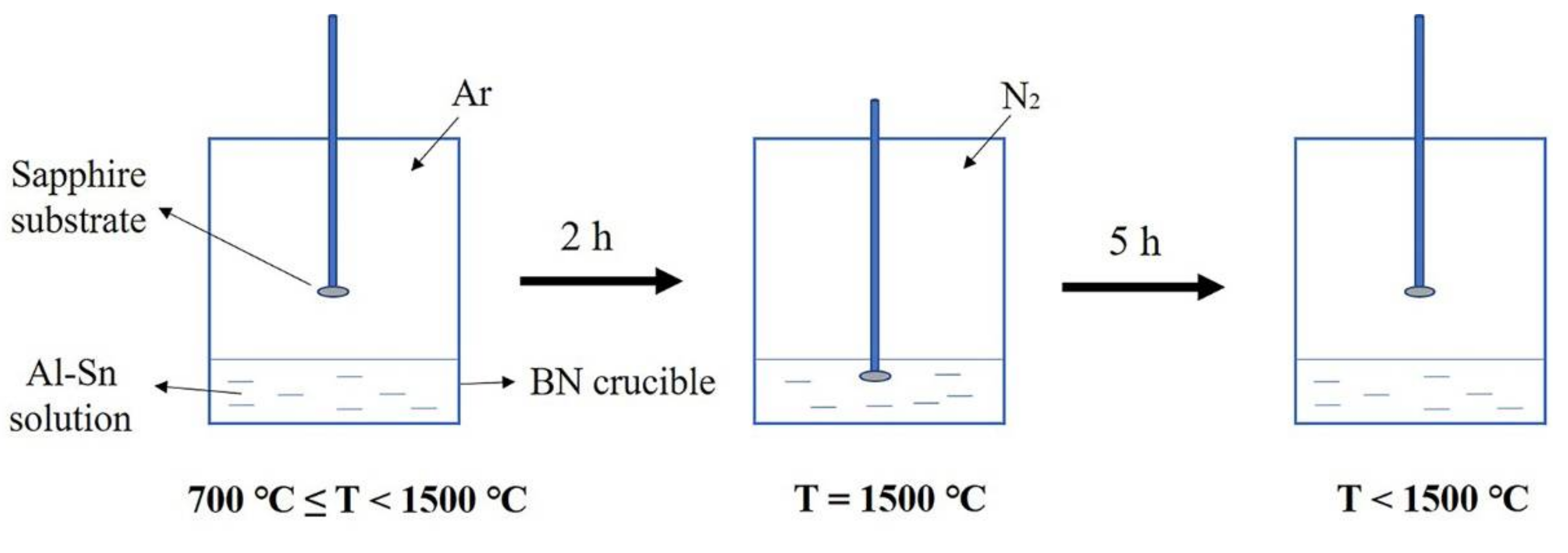
Figure 1 shows the experimental flow chart. First, Al and Sn particles were mixed in a PBN crucible with a molar ratio of 3:7. The PBN crucible was placed in a homemade induction furnace, which was vacuumed to below 10−3 KPa to remove residual oxygen and moisture. Then, the furnace temperature was raised to 700 °C and pure argon with a partial pressure of 34 KPa was introduced. Additionally, the furnace temperature was then further elevated at a rate of 6.7 °C/min. After two hours, the temperature reached 1500 °C. During this process, the sapphire substrate remained above the solution. When the temperature reached 1500 °C, N2 with a partial pressure of 67 KPa was introduced. Subsequently, a sapphire substrate was dipped into the Al-Sn solution and kept for 5 h under 1500 °C. After five hours, the sapphire substrate was lifted and the furnace began to cool at a rate of 4 °C/min until it returned to room temperature. After being grown, the product was corroded with aqua regia to remove the metal covering the surface. After pickling, the product was characterized.
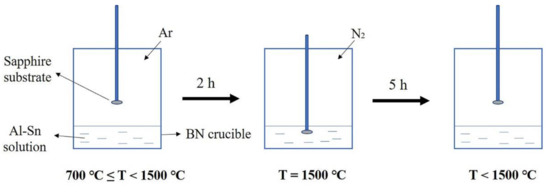
Figure 1.
Experimental flow chart.
3. Results and Discussion
3.1. The Morphological and Crystallization Quality of AlN Nanowires
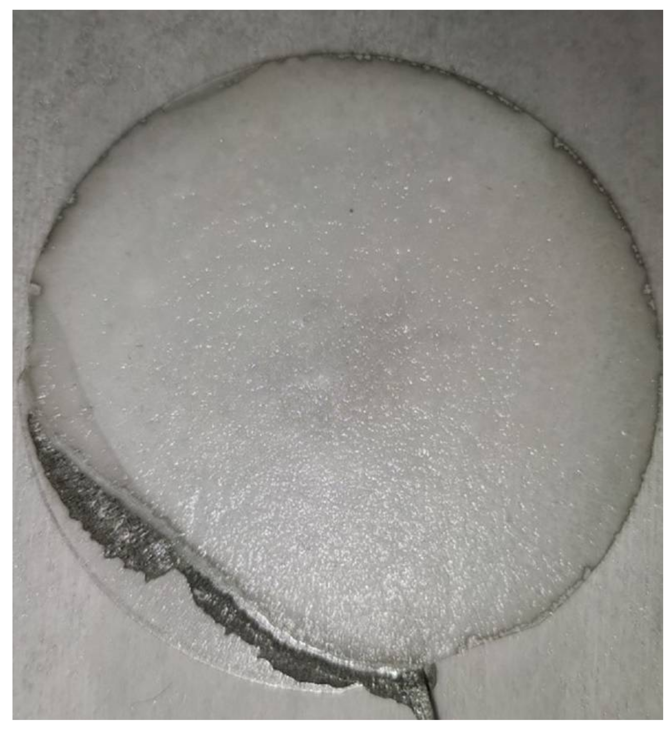
Figure 2 shows a picture of AlN nanowires on the sapphire after corrosion by aqua regia. A large amount of gray-white product was evenly distributed and formed a thin film covering the sapphire substrate. There was some residual metal at the edge of the sapphire. This may have been due to the fact that it was not corroded completely.
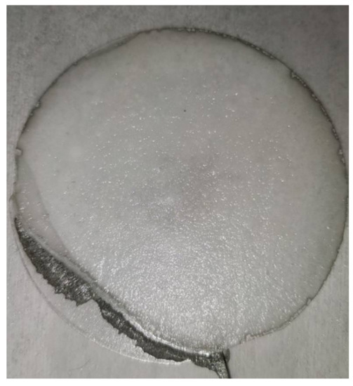
Figure 2.
A picture of AlN nanowires on the sapphire.
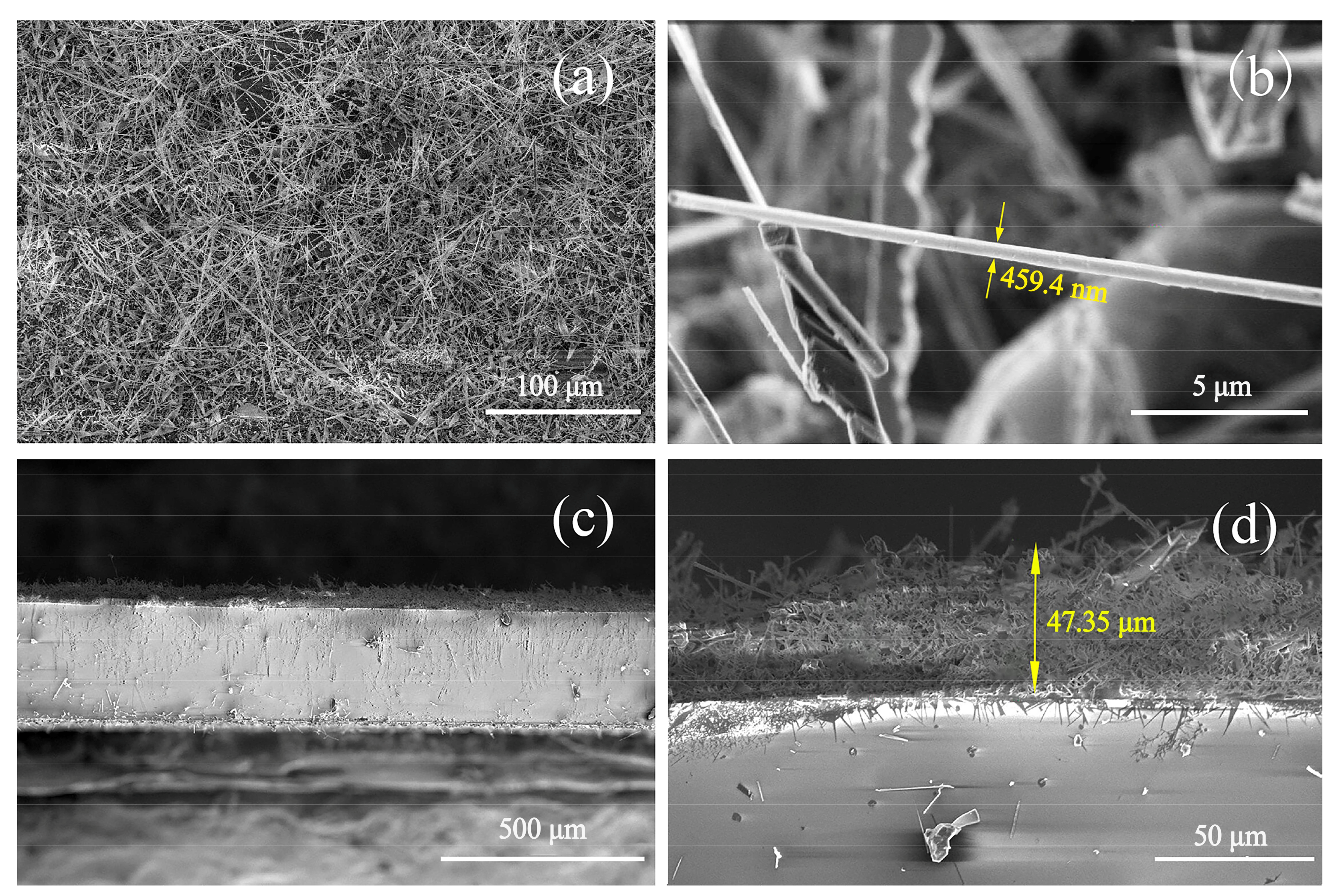
The morphology of AlN nanowires was observed by field emission scanning electron microscopy (FE-SEM), as shown in Figure 3. Obviously, Figure 3a shows a whole view of the AlN nanowires with high density, revealing that these nanowires did not grow along the same direction, but were stacked haphazardly across each other. The SEM image of a single AlN nanowire is shown in Figure 3b, from which it can be seen that the diameter of the nanowire is about 459 nm and the length of the nanowire is up to tens of microns. Figure 3c,d show side-view SEM images of the product. Figure 3d is a zoomed image of the yellow rectangular region of Figure 3c. As shown in Figure 3d, approximately 47.3 µm-thick AlN film was obtained on the sapphire substrate.
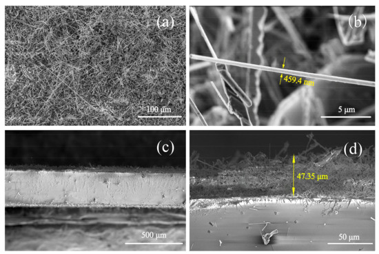
Figure 3.
(a) SEM image of the large-scale AlN nanowires; (b) SEM image of a single AlN nanowire; and (c,d) cross-sectional SEM images of AlN film.
The microstructure and crystal structure of AlN nanowires were further analyzed by transmission electron microscopy (TEM) and high-resolution TEM (HRTEM). From Figure 4a, it can be seen that the synthesized nanowire has a smooth surface and a diameter of around 223 nm. The energy dispersive spectrometer (EDS) spectrum in Figure 4b indicates that the chemical composition of the nanowire mainly contains N and Al elements with a small amount of other elements from the copper mesh. As can be seen from Figure 4c, the selected area electron diffraction (SAED) analysis of the nanowire was carried out with the TEM, which corresponded to a single AlN crystal with hexagonal wurtzite structure (ICDD-PDF No. 25-1133). From the HRTEM image in Figure 4d, it can be seen that the lattice distance of the nanowires is 0.25 nm, which matches well with the (002) plane of AlN, indicating that the growth direction is parallel to the (001) plane. Both the SAED pattern and the lattice spacing confirm the single structure of the nanowire.
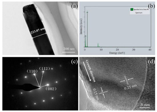
Figure 4.
(a) TEM image of a single AlN nanowire; (b) EDS analysis of the AlN nanowire; (c) SAED pattern of the AlN nanowire; and (d) HRTEM image of the AlN nanowire.
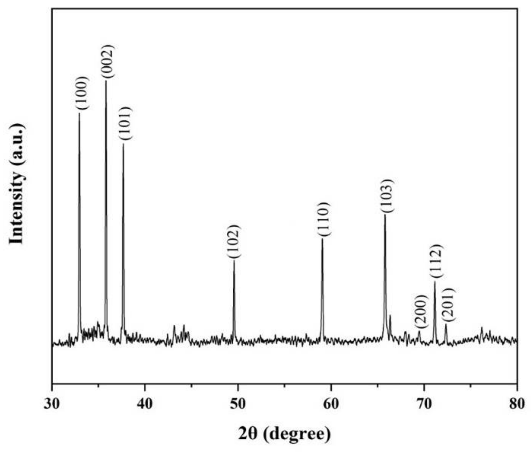
The crystal structure of the nanowires was characterized by the X-ray diffraction (XRD) with Cu Kα radiation in Figure 5. The nine diffraction peaks in Figure 5 are indexed to (100), (002), (101), (102), (110), (103), (200), (112) and (201) reflections of the hexagonal AlN, with lattice parameters of a = 3.111 Å, c = 4.979 Å (JCPDS card No. 25–1133). By gaussian fitting of the XRD spectrum, the full width at half maximum (FWHM) of (100), (002) and (101) were found to be 0.09706°, 0.08801°and 0.09564°, respectively. The narrow FWHM of these peaks certifies that AlN nanowires have good crystalline characteristics [11].

Figure 5.
The XRD pattern of AlN nanowires.
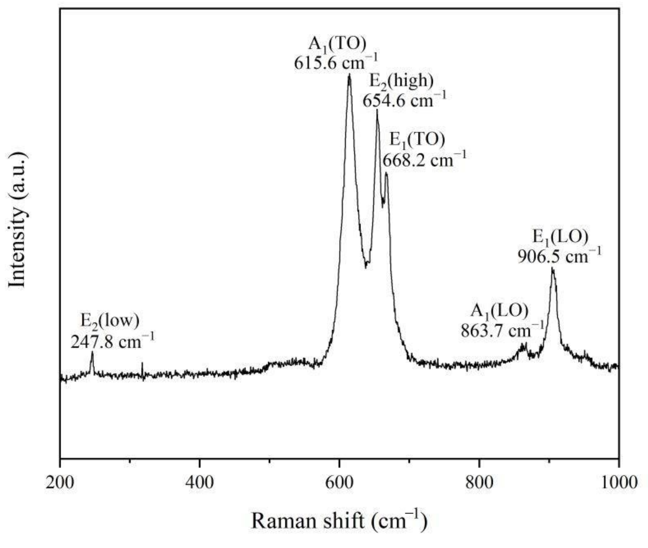
It is well known that Raman spectroscopy can be used to further study the crystalline quality by the phonon modes. AlN is a tetrahedral coordination compound with a hexagonal wurtzite crystal structure, and belongs to the (P63mc) space group. As shown in Figure 6, six signals at 247.8 cm−1, 615.6 cm−1, 654.6 cm−1, 668.2 cm−1, 863.7 cm−1 and 906.5 cm−1 correspond to the E2(low), A1(TO), E2(high), E1(TO), A1(LO) and E1(LO) phonon modes, which matches well with the space group of hexagonal aluminum nitride [12]. Compared with an AlN crystal, the Raman spectrum of AlN nanowires obtained in this experiment shows a slight redshift, which may be related to the size confinement effect, surface effect and internal stress of the nanomaterials [13,14,15]. In addition, it is thought that widened and asymmetrical Raman peaks may also be explained by the quantum size effect and internal stress [16].

Figure 6.
Room-temperature Raman scattering spectrum of AlN nanowires.
3.2. Absorption Spectrum and PL Spectrum of AlN Nanowires
The optical absorption spectrum of AlN nanowires was obtained by ultraviolet–visible (UV) spectroscopy. The absorption spectrum of AlN nanowires, which ranged from 190 nm to 400 nm, is shown in Figure 7. There is a significant absorption peak at 199 nm, matching the AlN bandgap of 6.23 eV. In addition, two wider absorption peaks were observed at 219 nm and 237 nm, which may be attributed to nitrogen vacancies and oxygen-related defects [17]. However, we emphasize here that the two absorption peaks are located in the UV-C spectral region, which is the most relevant to medical applications [18]. For example, UV-C LEDs are used for disinfection and purification.
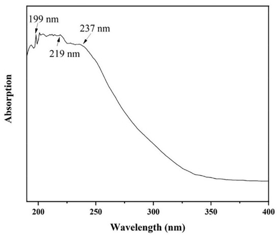
Figure 7.
The absorption spectrum of AlN nanowires.
The luminescence properties of AlN nanowires were investigated by PL spectrogram with a 532 nm laser. As can be seen from Figure 8, there is a very wide absorption peak ranging from 530 nm to 830 nm, and the center of the absorption peak is 657 nm. In addition, there are several weak defect-level emission peaks at about 552, 571, and 610 nm. These luminescence peaks may be generated by a few defect levels inside the AlN bandgap [19]. The emission peak at 657 nm (1.90 eV) is possibly due to the electronic transition from the deep level of VAl-ON to the valence band [20]. The emission peak at 552 nm (2.25 eV) may be due to the transition of the defect level generated by VAl to the top of the valence band [21,22]. The luminescence peak at 571 nm (2.18 eV) may be related to the transition from the ON-ON defect pair to the complex defect level produced by VAl-2ON. Additionally, the emission peak at 610 nm (2.04 eV) can be ascribed to the transition from the conduction band to the impurity level associated with oxygen (IO) [23].
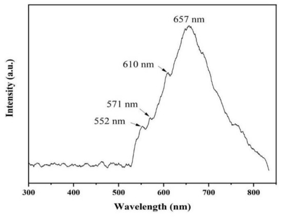
Figure 8.
Room-temperature PL spectrum of AlN nanowires.
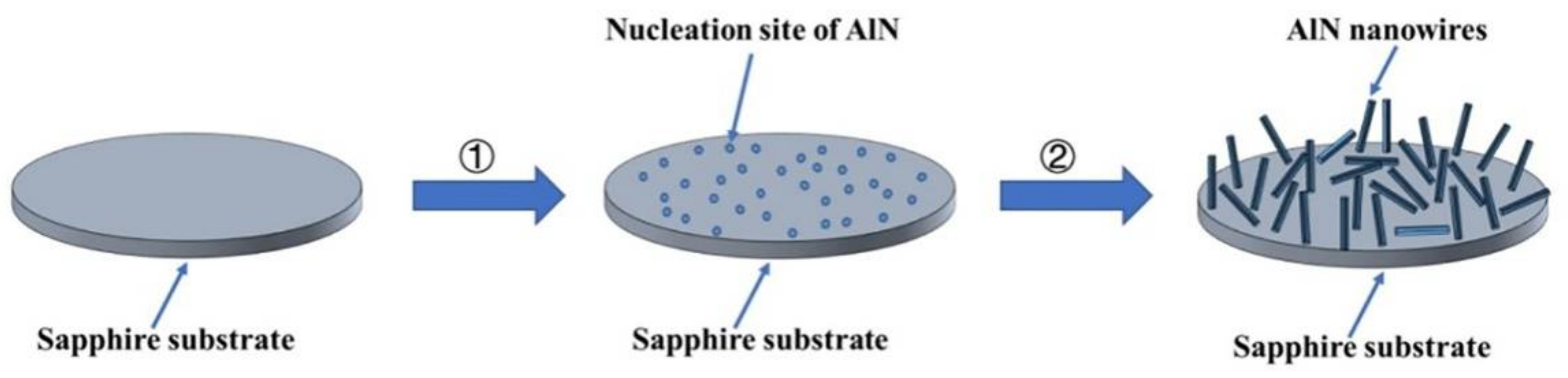
3.3. The Growth Mechanism of AlN Nanowires
As shown in Figure 9, the growth process of AlN nanowires can be divided into two steps: (1) the formation of the nucleation site of AlN, and (2) the growth process of AlN nanowires. Because the heater and insulation blanket are graphite components, carbon reacts with oxygen to form carbon monoxide when oxygen is insufficient (Equation (1)). Carbon monoxide reduces alumina to an Al gas or oxide with low-price Al (Equations (2)–(4)), and then aluminum-containing gas reacts with nitrogen gas to produce AlN (Equations (5)–(7)) [24]. This formed the nucleation site of AlN on the sapphire surface, and then AlN nanowires grew on the nucleation site. The nucleation sites of AlN then constantly absorbed Al and N atoms, and the AlN crystal grew gradually to form nanowires. In the growth process, the nucleation point of AlN is not caused by the direct nitriding of sapphire, so the growth direction of AlN nanowires is independent of substrate orientation.
2C (s) + O2 (g) = 2CO (g)
Al2O3 (s) + 2CO (g) = Al2O (g) + 2CO2 (g)
2Al2O3 (s) + 6CO (g) = 4Al (g) + 6CO2 (g)
Al2O3 (s) + CO (g) = 2AlO (g) + CO2 (g)
Al2O (g) + N2 (g) = 2AlN (s) + 1/2O2 (g)
Al2O (g) + CO (g) + N2 (g) = 2AlN (s) + CO2 (g)
2Al (g) + N2 (g) = 2AlN (s)
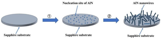
Figure 9.
Schematic illustration of the growth process for AlN nanowires.
4. Conclusions
In summary, AlN nanowires tens of microns in length and hundreds of nanometers in diameter were successfully synthesized by the Al-Sn flux method at 1500 °C for 5 h. The results show that the growth direction of aluminum nitride nanowire is parallel to the (001) planes. The UV studies indicate that AlN nanowires have a promising future in the UV-C devices field. The PL spectrum exhibits a broad emission peak with several weak peaks, which may be ascribed to the electronic transition between defect levels of the AlN bandgap.
Author Contributions
Conceptualization, Y.X.; investigation, H.M. and L.L.; resources, Y.X., L.L. and Y.Y.; data curation, W.M. and X.Q.; writing—original draft preparation, H.M.; writing—review and editing, J.C.; supervision, Z.H.; project administration, Y.X. All authors have read and agreed to the published version of the manuscript.
Funding
This research was funded by the Young Scientist Fund of NSFC, grant number 52002275, and the Scientific Research Foundation of Tianjin University of Technology.
Institutional Review Board Statement
Not applicable.
Informed Consent Statement
Not applicable.
Data Availability Statement
Not applicable.
Conflicts of Interest
The authors declare no conflict of interest.
References
- Taniyasu, Y.; Kasu, M.; Makimoto, T. An aluminium nitride light-emitting diode with a wavelength of 210 nanometer. Nature 2006, 441, 325–328. [Google Scholar] [CrossRef] [PubMed]
- Ambacher, O. Growth and applications of Group III-nitrides. J. Phys. D Appl. Phys. 1998, 31, 2653. [Google Scholar] [CrossRef]
- Slack, G.A.; Tanzilli, R.; Pohl, R.; Vandersande, J. The intrinsic thermal conductivity of AlN. J. Phys. Chem. Solids 1987, 48, 641–647. [Google Scholar] [CrossRef]
- Tavsanoglu, T. Synthesis of c-axis oriented AlN thin films at room temperature. Surf. Eng. 2017, 33, 249–254. [Google Scholar] [CrossRef]
- Isobe, H.; Kawamura, F.; Kawahara, M.; Yoshimura, M.; Mori, Y.; Sasaki, T. Synthesis of AlN Grains and Liquid-Phase-Epitaxy (LPE) Growth of AlN Films Using Sn-Ca Mixed Flux. Jpn. J. Appl. Phys. 2005, 44, L488–L490. [Google Scholar] [CrossRef]
- Li, H.; Wang, W.; Song, B.; Wu, R.; Li, J.; Sun, Y.; Zheng, Y.; Jian, J. Catalyst-free synthesis, morphology evolution and optical property of one-dimensional aluminum nitride nanostructure arrays. J. Alloys Compd. 2010, 503, L34–L39. [Google Scholar] [CrossRef]
- Li, C.L. Strong cathodoluminescence of AlN nanowires synthesized by aluminum and nitrogen. Mater. Lett. 2014, 115, 212–214. [Google Scholar] [CrossRef]
- Lei, M.; Song, B.; Guo, X.; Guo, Y.; Li, P.; Tang, W. Large-scale AlN nanowires synthesized by direct sublimation method. J. Eur. Ceram. Soc. 2008, 29, 195–200. [Google Scholar] [CrossRef]
- Zheng, M.; Jia, Q.; Liu, X.; Jia, G. Synthesis of ultra-long aluminum nitride nanowires with excellent photoluminescent property by aluminum chloride assisted chemical vapor reaction technique. Ceram. Int. 2019, 45, 12387–12392. [Google Scholar] [CrossRef]
- Shen, L.; Cheng, T.; Wu, L.; Li, X.; Cui, Q. Synthesis and optical properties of aluminum nitride nanowires prepared by arc discharge method. J. Alloys Compd. 2007, 465, 562–566. [Google Scholar] [CrossRef]
- Zheng, M.; Jia, Q.; Zhu, S.; Liu, X. Large scale synthesis and photoluminescent property of ultra-long AlN nanowires via a NH 4 Cl assisted chemical vapor reaction method. Ceram. Int. 2018, 44, 7267–7272. [Google Scholar] [CrossRef]
- Wang, G.; Chen, C.; Shao, Y.; Chen, F.; Zhang, L.; Wu, Y.; Hao, X. High-aspect-ratio single-crystalline AlN nanowires: Free-catalytic PVT growth and field-emission studies. J. Alloys Compd. 2019, 794, 171–177. [Google Scholar] [CrossRef]
- Sumathi, R.R.; Barz, R.U.; Gigler, A.M.; Straubinger, T.; Gille, P. Growth of AlN bulk single crystals on 4H-SiC substrates and analyses of their structural quality and growth mode evolution. Phys. Status Solidi A Appl. Mater. Sci. 2012, 209, 415–418. [Google Scholar] [CrossRef]
- Lei, M.; Yang, H.; Guo, Y.; Song, B.; Li, P.; Tang, W. Synthesis and optical property of high purity AlN nanowires. Mater. Sci. Eng. B 2007, 143, 85–89. [Google Scholar] [CrossRef]
- Shen, L.; Li, X.; Zhang, J.; Ma, Y.; Wang, F.; Peng, G.; Cui, Q.; Zou, G. Synthesis of single-crystalline wurtzite aluminum nitride nanowires by direct arc discharge. Appl. Phys. A 2006, 84, 73–75. [Google Scholar] [CrossRef]
- Lyu, S.; Cha, O.; Suh, E.-K.; Ruh, H.; Lee, H.; Lee, C. Catalytic synthesis and photoluminescence of gallium nitride nanowires. Chem. Phys. Lett. 2003, 367, 136–140. [Google Scholar] [CrossRef]
- Irmscher, K.; Hartmann, C.; Guguschev, C.; Pietsch, M.; Wollweber, J.; Bickermann, M. Identification of a tri-carbon defect and its relation to the ultraviolet absorption in aluminum nitride. J. Appl. Phys. 2013, 114, 390–447. [Google Scholar] [CrossRef]
- Tillner, N.; Frankerl, C.; Nippert, F.; Davies, M.J.; Brandl, C.; Lösing, R.; Mandl, M.; Lugauer, H.-J.; Zeisel, R.; Hoffmann, A.; et al. Point Defect-Induced UV-C Absorption in Aluminum Nitride Epitaxial Layers Grown on Sapphire Substrates by Metal-Organic Chemical Vapor Deposition. Phys. Status Solidi (b) 2020, 257, 2000278. [Google Scholar] [CrossRef]
- Yamane, T.; Murakami, H.; Kangawa, Y.; Kumagai, Y.; Koukitu, A. Growth of thick AlN layer on sapphire (0001) substrate using hydride vapor phase epitaxy. Phys. Status Solidi (c) 2005, 2, 2062–2065. [Google Scholar] [CrossRef]
- Cao, Y.; Chen, X.; Lan, Y.; Li, J.; Xu, Y.; Xu, T.; Liu, Q.; Liang, J. Blue emission and Raman scattering spectrum from AlN nanocrystalline powders. J. Cryst. Growth 2000, 213, 198–202. [Google Scholar] [CrossRef]
- Chichibu, S.F.; Hazu, K.; Ishikawa, Y.; Tashiro, M.; Ohtomo, T.; Furusawa, K.; Uedono, A.; Mita, S.; Xie, J.; Collazo, R.; et al. Excitonic emission dynamics in homoepitaxial AlN films studied using polarized and spatio-time-resolved cathodoluminescence measurements. Appl. Phys. Lett. 2013, 103, 142103. [Google Scholar] [CrossRef]
- Sedhain, A.; Lin, J.Y.; Jiang, H.X. Nature of optical transitions involving cation vacancies and complexes in AlN and AlGaN. Appl. Phys. Lett. 2012, 100, 221107. [Google Scholar] [CrossRef] [Green Version]
- Yuwen, M.; Liu, J.; Xia, C.; Liu, Z.; Yu, C.; Li, H. Novel single-host Al1−xSixCxN1−x: Mn2+ white phosphors for field emission displays. J. Mater. Sci. Mater. Electron. 2017, 28, 8405–8413. [Google Scholar] [CrossRef]
- Yu, J.; Ueno, S.; Li, H.; Hiragushi, K. Improvement of graphitization of isotropic carbon by Al2O3 formed from aluminium chelate compound. J. Eur. Ceram. Soc. 1999, 19, 2843–2848. [Google Scholar] [CrossRef]


Publisher’s Note: MDPI stays neutral with regard to jurisdictional claims in published maps and institutional affiliations. |
© 2022 by the authors. Licensee MDPI, Basel, Switzerland. This article is an open access article distributed under the terms and conditions of the Creative Commons Attribution (CC BY) license (https://creativecommons.org/licenses/by/4.0/).