Abstract
The state-of-the-art silicon insulated-gate bipolar transistor (IGBT) features a trench gate, since it enhances the conductivity modulation. The SiC trench IGBT, however, faces the critical challenge of a high electric field in the gate oxide, which is a crucial threat to the device’s reliability. In this work, we explore the possibility of using a SiC planar IGBT structure to approach high performance to the level of a SiC trench IGBT, without suffering the high gate oxide field. The proposed SiC planar IGBT features buried p-layers directly under the p-bodies, and thus can be formed using the same mask set. The region between the buried p-layer and the p-body is heavily doped with n-type dopants so that the conductivity modulation is improved. Comprehensive TCAD simulations have been carried out to verify this concept, and the simulation results show the new SiC planar IGBT exhibits a high performance comparable to the trench IGBT, and also exhibits a low gate oxide field.
Keywords:
SiC; IGBT; trench-gate; planar-gate; buried p-layers; high performance; low gate oxide field 1. Introduction
Due to the excellent material properties (wide bandgap, a high critical electric field, a high temperature endurance, etc.), silicon carbide (SiC) is attractive for power devices such as the Schottky barrier diode, the metal–oxide–semiconductor field effect transistor (MOSFET), and the insulated-gate bipolar transistor (IGBT) [1,2,3,4].
SiC IGBT is welcomed in ultrahigh voltage power applications because the conductivity modulation in IGBTs can effectively reduce conduction loss [5,6,7,8]. For traditional silicon IGBTs, the trench-gate structure is the state-of-the-art technology, which takes advantage of the injection enhancement effect that further improves the conductivity modulation at the top side of the device [9,10]. However, SiC trench-gate devices face the issue of a high gate oxide field in the off-state [11].
In a conventional SiC planar IGBT, the gate oxide field is often low enough. The grounded p-body in the conventional SiC planar IGBT helps to protect the planar-gate. The drawback of the SiC planar IGBT is the compromised conductivity modulation, which is caused by the grounded p-bodies that extract minority carriers [9,12]. This compromised conductivity modulation will cause considerable increase of the on-state voltage (VON) and conduction power loss.
In this paper, we explore the possibility of using a SiC planar IGBT structure to approach a high performance comparable to the SiC trench IGBT, and at the same time, to maintain a low gate oxide field. A new SiC planar IGBT (BP-IGBT) with buried p-layers under the p-body is proposed. The buried p-layers are aligned with p-bodies, and thus they can share the same mask set. Numerical simulation results show the BP-IGBT obtains a low VON close to the SiC trench IGBT. The breakdown voltage (BV) of the BP-IGBT is kept nearly the same as the SiC trench IGBT. The maximum gate oxide field in the BP-IGBT is dramatically lower than that in the SiC trench IGBT.
Sentaurus TCAD tools are used for the simulations [13]. Sentaurus Structure Editor is used for structure and mesh construction. The mesh of the device consists of a coarse mesh definition and several refined mesh definitions. The coarse mesh is placed for the whole device with lateral/vertical mesh sizes of 0.4/0.6 µm. The top 10-µm region of the device is fitted with a refined mesh with lateral/vertical mesh sizes of 0.1/0.2 µm. The PN junctions are further refined with a mesh size of ~0.02 µm along the direction perpendicular to the junction. At the oxide/semiconductor interfaces, the mesh size along the direction perpendicular to the interface is refined to 0.002 µm. The Sentaurus Device is used for device simulations and mixed-mode circuit simulations. In device simulations, the Poisson equation and electron/hole continuity equations are solved self-consistently. In mixed-mode circuit simulations, the circuit equations are also solved in the same manners as traditional SPICE tools. The physics models, including the Auger and Shockley–Reed–Hall combinations; impact ionization (Lackner model); incomplete ionization; the high-field saturation effect; doping dependent transport; band narrowing; and the anisotropic mobility model are all considered.
2. Device Structure and Proposed Process Flow
Figure 1 shows the cross-sectional schematic views of the studied conventional SiC planar IGBT (P-IGBT), SiC trench IGBT (T-IGBT), and the proposed buried p-layer IGBT (BP-IGBT). A heavily doped n-type region is located between the buried p-layer and the p-body in the BP-IGBT. The devices are designed for a 20-kV voltage level. The trench gate in the T-IGBT has a width of 1.5 μm and rounded bottom gate corners with a radius of 0.2 μm. The buried p-layer in the BP-IGBT has a doping density of 1 × 1018 cm−3 to avoid being fully depleted in the off-state. The distance between neighboring p-bodies or neighboring buried p-layers is 2 μm. The channel mobility is set to be 30 cm2/V-s. The channel length is 1 μm. The devices are designed for 20-kV voltage rating. The device parameters are carefully chosen based on the state-of-the-art SiC IGBTs and MOSFETs [5,6,7,8,9,10,14,15]. Table 1 lists the key device parameters used in this work.
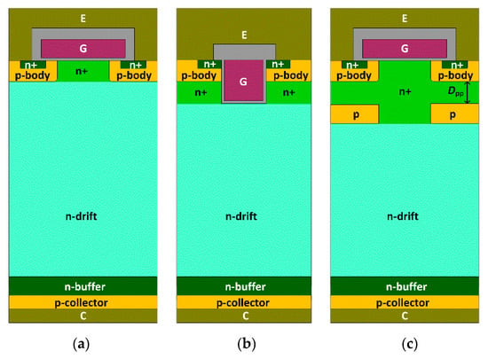
Figure 1.
Schematic cross-sections of (a) SiC planar insulated-gate bipolar transistor (IGBT) (P-IGBT), (b) the SiC trench IGBT (T-IGBT), and (c) the new SiC planar IGBT with buried p-layers (BP-IGBT).

Table 1.
Key structural parameters of the studied SiC IGBTs.
The fabrication method of the proposed BP-IGBT is similar to the P-IGBT, except for the buried p-layers. A proposed fabrication process flow is shown in Figure 2. After growth of the drift layer and n+ layer, the buried p-layers can be formed by ion-implantation. Then, a second n+ layer is regrown. The surface structure can be formed in the same way as a traditional SiC IGBT, which includes implantation for the p-body and n+-emitter region, formation of the MOS-structure, contact holes for the emitter, and metallization. For SiC technology, formation of buried p-layers is a practically viable process, and has been reported in literature [16,17]. Therefore, the proposed structure in this paper is a technically feasible solution for the SiC IGBT.
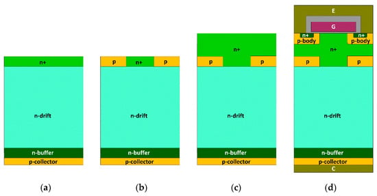
Figure 2.
Proposed fabrication process flow for the BP-IGBT. (a) Formation of epitaxial layers. (b) Formation of the buried p-layer by ion-implantation. (c) Regrowth of the n+ layer. (d) Formation of the surface structure in the same way as a traditional SiC IGBT.
3. Device Characteristics
The vertical distance (Dpp) between the p-body and the buried p-layer in the BP-IGBT is critical to the device’s performances. Figure 3 shows the influence of Dpp on VON and BV for the BP-IGBT. Here, VON is defined as the collector voltage with IC = 50 A/cm2 and VGE = 15 V. BV is defined as the collector voltage with IC = 1 A/cm2 and VGE = 0 V. VON decreases with larger Dpp, because the heavily doped n+-region is beneficial for increasing conductivity modulation in the IGBT. As for the BV, when Dpp is smaller than 6.5 μm, a stably higher BV (>25 kV) is obtained. Then, if the buried p-layer is much deeper, BV degrades quickly as premature breakdown happens at the p-body/n+-region junction. Thus, in the following study, Dpp = 5 μm is adopted to leave enough of a margin for a stably high BV.
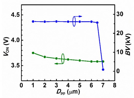
Figure 3.
The influence of distance between the p-body and the buried p-layer (Dpp) on VON and BV for the proposed BP-IGBT.
Figure 4 plots the forward IC–VCE characteristics of the SiC IGBTs. The VON of the proposed BP-IGBT is only 3.6 V, close to the 3.4 V of the T-IGBT. This is because the BP-IGBT obtains an enhanced conductivity modulation induced by the heavily doped n+-region at the top side. The P-IGBT suffers a much higher VON of 5.2 V as the grounded p-body extracts holes around it.
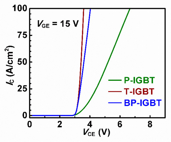
Figure 4.
IC–VCE characteristics of the studied SiC IGBTs.
The enhanced conductivity modulation in the BP-IGBT and T-IGBT can be evidenced by the hole density, as is displayed in Figure 5. At the lower side of the IGBTs, all of them exhibit a similar hole density distribution. At the topside, the BP-IGBT obtains a high hole density to the same level of the T-IGB, while the P-IGBT shows an obviously decreased hole density. The grounded p-body in the P-IGBT presents a low barrier for holes, and thus quickly extracts holes and causes a low hole density. For the T-IGBT, the protruded trench gate creates an energy barrier for the holes and screens the p-body from extracting holes, which leads to a high density of holes at the topside of the device. For this purpose, a small cell size of the T-IGBT is preferable since the p-body is better screened by the gate [9,18,19]. For the proposed BP-IGBT, the n+-region under the p-body creates an energy barrier for holes, and also results in a high hole density.
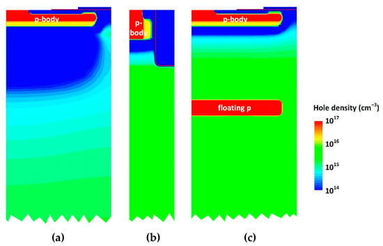
Figure 5.
Hole density distribution of (a) P-IGBT, (b) T-IGBT, and (c) the new BP-IGBT under IC = 50 A/cm2.
The BV capabilities under VGE = 0 V are plotted in Figure 6a. All the studied SiC IGBTs exhibit a nearly same BV of ~26.5 kV. The BV is mainly determined by the thickness and doping of the n-drift region. The difference in the top structure just slightly changes the BV. In the P-IGBT and T-IGBT, the BV is supported by the PN junction below the p-body. While in the proposed BP-IGBT, the BV is mainly sustained by the p-shield/n-drift junction, as the n+-layer below the p-body is depleted under a small voltage. For the SiC planar IGBT with only the n+-region but no buried p-layer, the BV is less than 2 kV as the n+-region tends to increase the electric field at the p-body/n junction. The buried p-layer can overcome the problem caused by the n+-region, so a low VON and a high BV can be simultaneously obtained in the BP-IGBT.
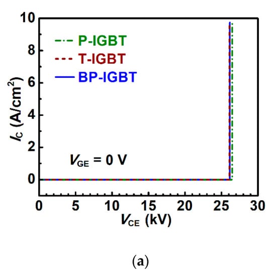
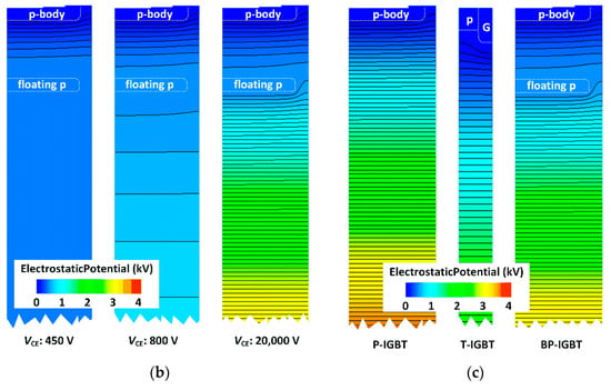
Figure 6.
(a) BV characteristics of the P-IGBT, T-IGBT, and BP-IGBT under VGE = 0 V. (b) Equipotential lines (step = 50 V) of the BP-IGBT under different VCE in the off-state: VCE = 450 V, VCE = 800 V, and VCE = 20,000 V. (c) Equipotential lines (step = 50 V) of the studied IGBTs under VCE = 20,000 V.
Figure 6b further depicts the process in the BP-IGBT using potential contour. With the rise of VCE, in the beginning, the voltage is first supported by the PN junction below the p-body, as shown in Figure 6b (VCE = 450 V). When the n+-region is depleted, the potential of the buried p-layer is clamped, and the rest of the voltage is supported by the PN junction below buried p-layers, as shown in Figure 6b (VCE = 800 V and VCE = 20,000 V). This analysis also explains the dependence of BV on Dpp in Figure 3. Therefore, the blocking mechanism of the BP-IGBT is different to the conventional P-IGBT and T-IGBT. As shown in Figure 6c, in the conventional IGBTs without buried p-layers, the p-body/n junction and/or MOS junction support the whole off-state voltage. The electric field is highest near the p-body/n junction, and/or MOS junction, where the equipotential lines are most crowded.
The gate oxide field distribution in the off-state of the SiC IGBTs are displayed in Figure 7. As the gate protrudes downward, the T-IGBT suffers an extremely large oxide field (Eox-m) of ~8 MV/cm, which presents a serious threat on the device’s long-term reliability [20]. In this study, the radius of the gate trench corner is 0.2 µm. The maximum oxide field (Eox-m) of the T-IGBT is dependent on the shape of the trench corner. With the radius of the trench corner changing from 0.1 µm to 0.5 µm, the Eox-m reduces from 9.76 MV/cm to 7.58 MV/cm. Therefore, a rounded trench corner helps to relieve the electric field stress in the gate oxide, but cannot overcome this problem. While in the P-IGBT and the proposed BP-IGBT, the planar-gate structures help to decrease the Eox-m to a safe level of below 3 MV/cm.
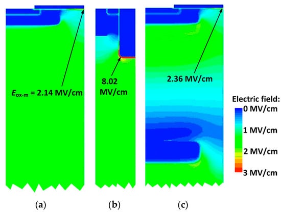
Figure 7.
Electric field distribution in (a) P-IGBT, (b) T-IGBT, and (c) BP-IGBT at VCE = 20 kV and VGE = −5 V.
Introducing floating p-layers in the unipolar SiC MOSFETs is found to cause a storage of negative charges and a degradation of dynamic VON [21,22]. But for IGBTs with bipolar conduction, the stored negative charges in the off-state can be neutralized in the following on-state, by the holes injected from p-collector. The dynamic VON characteristics of the BP-IGBT are also studied in this paper and are shown in Figure 8. Mixed-mode TCAD simulations are utilized. The schematic circuit used for switching characteristics is shown in Figure 8a. The supply voltage is 13 kV. The stray inductance is assumed to be 10 nH in the power loop. The chip area of the device under test (DUT) is set to be 1 cm2. To turn the device on and off, the gate to emitter voltage is switched between +15 V and −5 V.
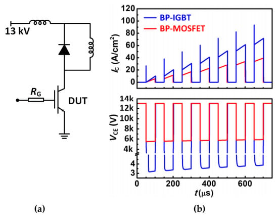
Figure 8.
(a) Schematic circuit used for the switching characteristics. (b) The switching waveforms of the BP-IGBT and BP-MOSFET experiencing multiple switching cycles.
The multi-cycle switching waveforms are plotted in Figure 8b. For comparison, the dynamic VON characteristics of the corresponding SiC MOSFET (BP-MOSFET) are also studied. The BP-MOSFET is designed for the same voltage rating as the BP-IGBT by replacing the p-collector with the n-drain. For the BP-MOSFET, when the device experiences a high voltage in the off-state, the buried p-layers support a large portion of the voltage, and the p-layers become negatively charged. When the device returns to the on-state, the negative charged p-layers possess a negative potential, and the negative charges cannot be released through the negatively biased PN junctions. Therefore, the negative charges lead to an expansion of depletion regions, which significantly impedes the current flow and results in a VCE as high as 5.5 kV [21,22]. The BP-IGBT is a bipolar device. For the BP-IGBT, when it returns to the on-state, the large amount of positively charged holes can quickly eliminate the negative charges in the buried p-layers. Therefore, the BP-IGBT does not suffer degraded dynamic VON. The VON at IC = 50 A/cm2 in this Figure 8b is the same as the static condition in Figure 4.
With the schematic circuit in Figure 8a, the turn-off characteristics of the studied SiC IGBTs are studied and shown in Figure 9. The load current is 50 A/cm2. The turn-off loss (EOFF) of the devices can be obtained by integrating the power generation (VCE × IC) from 0 to 6 μs from Figure 9. The EOFF is normalized to the device area. EOFF is 0.65 J/cm2 for the P-IGBT, 0.65 J/cm2 for the T-IGBT, and 0.62 J/cm2 for the BP-IGBT. Although in the on-state, the T-IGBT and BP-IGBT feature a much higher hole density at the top side of the device compared to the P-IGBT, the EOFF values of all the devices are nearly same. This is because at the initial stage of the turn-off transient, the holes at the topside of the IGBT are first removed. For this period, the VCE is still very small, so it does not appreciably influence the EOFF. The hole density at the bottom side of the device has a much higher influence on EOFF, since when these holes are removed, VCE is also very large. In the figure, VCE of the P-IGBT and the proposed BP-IGBT start to rise before the T-IGBT, because the gate to collector capacitance of the P-IGBT and the BP-IGBT is smaller. However, this feature does not affect the EOFF of the devices.
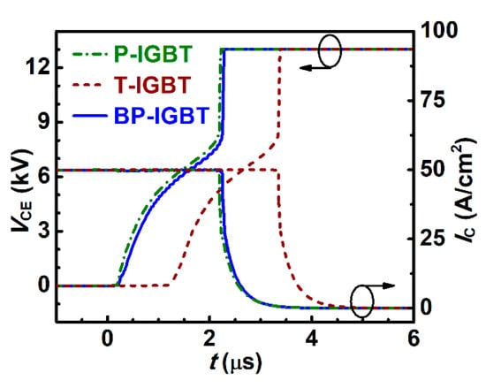
Figure 9.
Turn-off waveforms of the P-IGBT, the T-IGBT, and the proposed BP-IGBT.
The main device characteristics of the three devices are listed in Table 2 for comparison. The proposed BP-IGBT obtains high performance, to the level of the SiC trench IGBT, and is a promising candidate of power switches in ultrahigh voltage power applications.

Table 2.
Comparison of the device characteristics.
4. Conclusions
In this paper, we use a new SiC planar IGBT (BP-IGBT) to approach the high performance level of a SiC trench IGBT (T-IGBT). The proposed BP-IGBT features buried p-layers and obtains a low on-state voltage (VON) of 3.6 V, close to the 3.4 V of the T-IGBT. The buried p-layer is aligned with the p-body, and thus they can share the same mask set. The breakdown voltage of the BP-IGBT is nearly the same as the T-IGBT. The proposed BP-IGBT avoids a high off-state gate oxide field, which often is an issue in the T-IGBT. The dynamic VON characteristics of the BP-IGBT are not degraded.
Author Contributions
Conceptualization, M.Z. and J.W.; software, M.Z. and J.W.; investigation, M.Z.; writing—original draft preparation, M.Z.; writing—review and editing, B.L. and J.W.; supervision, B.L.; project administration, B.L. All authors have read and agreed to the published version of the manuscript.
Funding
This research was supported by the National Natural Science Foundation of China under Grant 51907127 and Grant 61604098, by the Shenzhen Science and Technology Innovation Commission under Grant JCYJ20170412110137562, and also by the Shenzhen University Scientific Research Start-up Foundation under Grant 860-000002110207.
Conflicts of Interest
The authors declare no conflict of interest.
References
- Kimoto, T.; Cooper, J.A. Fundamentals of Silicon Carbide Technology: Growth, Characterization, Devices and Applications; Wiley: Singapore, 2014. [Google Scholar]
- Capan, I.; Yamazaki, Y.; Oki, Y.; Brodar, T.; Makino, T.; Ohshima, T. Minority carrier trap in n-type 4H–SiC Schottky barrier diodes. Crystals 2019, 9, 328. [Google Scholar] [CrossRef]
- Lebedev, A.A.; Ber, B.Y.; Seredova, N.V.; Kazantsev, D.Y.; Kozlovski, V.V. Radiation-stimulated photoluminescence in electron irradiated 4H-SiC. J. Phys. D Appl. Phys. 2015, 48, 485106. [Google Scholar] [CrossRef]
- Daviau, K.; Lee, K.K.M. High-performance, high-temperature behavior of silicon carbide: A review. Crystals 2018, 8, 217. [Google Scholar] [CrossRef]
- Tiwari, A.K.; Antoniou, M.; Lophitis, N.; Perkins, S.; Udrea, F. Retrograde p-well for 10-kV class SiC IGBTs. IEEE Trans. Electron Devices 2019, 66, 3066–3072. [Google Scholar] [CrossRef]
- Brunt, E.V.; Cheng, L.; O’Loughlin, M.; Capell, C.; Jonas, C.; Lam, K.; Richmond, J.; Pala, V.; Ryu, S.; Allen, S.T.; et al. 22 kV 1 cm2 4H-SiC n-IGBTs with improved conductivity modulation. In Proceedings of the ISPSD, Waikoloa, HI, USA, 15–19 June 2014; pp. 358–361. [Google Scholar]
- Ryu, S.; Capell, C.; Jonas, C.; Cheng, L.; O’Loughlin, M.; Burk, A.; Agarwal, A.; Palmour, J.; Hefner, A. Ultra high voltage (>12 kV), high performance 4H-SiC IGBTs. In Proceedings of the ISPSD, Bruges, Belgium, 3–7 June 2012; pp. 257–260. [Google Scholar]
- Vechalapu, K.; Bhattacharya, S.; Van Brunt, E.; Ryu, S.; Grider, D.; Palmour, J.W. Comparative evaluation of 15-kV SiC MOSFET and 15-kV SiC IGBT for medium-voltage converter under the same dv/dt conditions. IEEE J. Emerg. Sel. Top. Power Electron 2017, 5, 469–489. [Google Scholar] [CrossRef]
- Kitagawa, M.; Omura, I.; Hasegawa, S.; Inoue, T.; Nakagawa, A. A 4500 V injection enhanced insulated gate bipolar transistor (IEGT) operating in a mode similar to a thyristor. In Proceedings of the IEEE International Electron Devices Meeting, Washington, DC, USA, 5–8 December 1993; pp. 679–682. [Google Scholar]
- Zhang, Q.; Chang, H.; Gomez, M.; Bui, C.; Hanna, E. 10 kV trench gate IGBTs on 4H-SiC. In Proceedings of the ISPSD, Santa Barbara, CA, USA, 23–26 May 2005; pp. 303–306. [Google Scholar]
- Zhang, M.; Wei, J.; Jiang, H.; Chen, K.J.; Cheng, C. SiC trench MOSFET with self-biased p-shield for low RON-SP and low OFF-state oxide field. IET Power Electron 2017, 10, 1208–1213. [Google Scholar] [CrossRef]
- Matsunaga, S.; Mizushima, T. Low Von 17kV SiC IGBT assisted n-MOS thyristor. In Proceedings of the IEEE International Electron Devices Meeting (IEDM), San Francisco, CA, USA, 7–11 December 2019; pp. 474–477. [Google Scholar]
- Synopsys. TCAD Sentaurus Device Manual; Synopsys Inc.: Mountain View, CA, USA, 2013. [Google Scholar]
- An, J.; Namai, M.; Tanabe, M.; Okamoto, D.; Yano, H.; Iwamuro, N. Experimental demonstration of −730V vertical SiC p-MOSFET with high short circuit withstand capability for complementary inverter applications. In Proceedings of the IEEE International Electron Devices Meeting (IEDM), San Francisco, CA, USA, 3–7 December 2016; pp. 272–275. [Google Scholar]
- Usman, M.; Nawaz, M. Device design assessment of 4H–SiC n-IGBT—A simulation study. Solid-State Electron. 2014, 92, 5–11. [Google Scholar] [CrossRef]
- Uchida, K.; Saitoh, Y.; Hiyoshi, T.; Masuda, T.; Wada, K.; Tamaso, H.; Hatayama, T.; Hiratsuka, K.; Tsuno, T.; Furumai, M.; et al. The optimised design and characterization of 1200 V/2.0 mΩ cm2 4H-SiC V-groove trench MOSFETs. In Proceedings of the ISPSD, Hong Kong, China, 10–14 May 2015; pp. 85–88. [Google Scholar]
- Nishio, J.; Ota, C.; Hatakeyama, T.; Shinohe, T.; Kojima, K.; Nishizawa, S.; Ohashi, H. Ultralow-loss SiC floating junction Schottky barrier diodes (super-SBDs). IEEE Trans. Electron Devices 2008, 55, 1954–1960. [Google Scholar] [CrossRef]
- Sumitomo, M.; Sakane, H.; Arakawa, K.; Higuchi, Y.; Matsui, M. Injection control technique for high speed switching with a double gate PNM-IGBT. In Proceedings of the ISPSD, Kanazawa, Japan, 26–30 May 2013; pp. 33–36. [Google Scholar]
- Zerarka, M.; Austin, P.; Bafleur, M. Comparative study of sensitive volume and triggering criteria of SEB in 600 V planar and trench IGBTs. Microelectron. Reliab. 2011, 51, 1990–1994. [Google Scholar] [CrossRef]
- Matocha, K.; Dunne, G.; Soloviev, S.; Beaupre, R. Time-dependent dielectric breakdown of 4H-SiC MOS capacitors and DMOSFETs. IEEE Trans. Electron Devices 2008, 55, 1830–1834. [Google Scholar] [CrossRef]
- Wei, J.; Zhang, M.; Jiang, H.; Wang, H.; Chen, K.J. Dynamic degradation in SiC trench MOSFET with a floating p-shield revealed with numerical simulations. IEEE Trans. Electron Devices 2017, 64, 2592–2598. [Google Scholar] [CrossRef]
- Takaya, H.; Miyagi, K.; Hamada, K. Floating islands and thick bottom oxide trench gate MOSFET (FITMOS) with passive hole gate. In Proceedings of the International Electron Devices Meeting, San Francisco, CA, USA, 11–13 December 2006; pp. 1–4. [Google Scholar]
© 2020 by the authors. Licensee MDPI, Basel, Switzerland. This article is an open access article distributed under the terms and conditions of the Creative Commons Attribution (CC BY) license (http://creativecommons.org/licenses/by/4.0/).