Article

Abrupt Change Effect of Bandgap Energy on Quantum System of Silicon Nanowire

1
College of materials and metallurgy, Institute of Nanophotonic Physics, Guizhou University, Guiyang 550025, China
2
State Key Laboratory of Environment Geochemistry, Institute of Geochemistry, Chinese Academy of Sciences, Guiyang 550003, China
3
Department of Physics, Hainan Normal University, Haikou 571158, China
*
Author to whom correspondence should be addressed.
Crystals 2020, 10(5), 340; https://doi.org/10.3390/cryst10050340
Submission received: 7 April 2020 / Revised: 23 April 2020 / Accepted: 24 April 2020 / Published: 26 April 2020
(This article belongs to the Special Issue Growth and Evaluation of Crystalline Silicon (Volume II))

Abstract

:
In the quantum system of Si nanowire (NW), the energy bandgap obviously increases with decreasing radius size of NW, in which the quantum confinement (QC) effect plays a main role. Furthermore, the simulation result demonstrated that the direct bandgap can be obtained as the NW diameter is smaller than 3 nm in Si NW with (001) direction. However, it is discovered in the simulating calculation that the QC effect disappears as the NW diameter arrives at size of monoatomic line, in which its bandgap sharply deceases where the abrupt change effect in bandgap energy occurs near the idea quantum wire. In the experiment, we fabricated the Si NW structure by using annealing and pulsed laser deposition methods, in which a novel way was used to control the radius size of Si NW by confining cylinder space of NW in nanolayer. It should have a good application on optic-electronic waveguide of silicon chip.

1. Introduction

Nanostructures, mainly involving nanoparticle, nanolayer and nanowire, have been studied intensively over the past decade [1,2,3,4,5]. Especially, scientists have made an attention to the nanowire (NW) structure because of its unique properties and a wide range of device applications in solid-state lighting, field effect transistor, integrated nanophotonics and nanoelectronics, and energy conversion [6,7,8,9,10,11,12,13]. Recently, in the quantum system of Si NW, some interesting phenomena and new effects have been discovered. For example, the quantum ballistic effect has been explored by Noboru Okamoto et al. (2019) in which the ballistic thermal transport in SiGe polycrystalline NW was investigate by measuring the length dependence of thermal conductivity in different alloy compositions and temperatures [14]. The core-multishell structure of NW was exploited by Marcus Meuller et al. (2019), in which advanced high-mobility NW transport channel was applied in optoelectronics and photonics integrations [15]. Furthermore, the effect of NW networks on the electrical and optical properties of conductive films was investigated by Fei Han et al. (2018), which provided insights that help optimizing random NW networks in transparent conductive films for achieving better efficiencies [16]. In this year, the NW nanocables were designed by Yong Sun et al. (2020) to be exploited for diverse applications in flexible electronics and complex wiring configurations [17].
It should be noted that the interesting phenomena and new effects occur in the quantum system of NW structure. In the article, we have investigated the quantum confinement (QC) effect in Si NW by using simulation method. It is interesting that the QC effect disappears as the NW diameter reaches to size of monoatomic line, where its bandgap sharply deceases. This abrupt change effect in bandgap energy may be originated from transforming between different dimensions at the symmetry broken point, in which the quasi-1D shape of NW is transformed to the one dimensional quantum wire. Here, the abrupt change effect in bandgap energy was observed and studied at first.

2. Fabrication of Silicon Nanowire

The popular methods in fabrication of silicon nanostructures were self-assembly ways from silicon-rich silicon oxide matrices [18,19,20] and plasma synthesis [21,22,23,24], in which the interesting method for fabricating silicon nanocrystal was growth under laser photons interaction [25,26,27]. In our experiment, the most interesting and simplest method discovered for fabricating silicon nanostructures was self-assembly growth in annealing process on the silicon amorphous nanofilm produced by using pulsed laser deposition (PLD) method [28].
The preparing process of silicon NW involves two steps, at first a Si amorphous nanofilm was produced by using PLD method, subsequent high-temperature annealing of the substoichimetric film (typically 900~1100 °C) generated crystallizing of nanoclusters in the nanofilm and produced a phase separation between Si crystal and amorphous with the formation of Si nanoparticles, in which silicon NW was gradually generated with connecting nanoparticles by controlling temperature and time of annealing, as shown in Figure 1.
In the experiment, a novel method was used to fabricate Si NW, in which the growth process of silicon NW was confined in the nanolayer of silicon. Here, a third harmonic of pulsed Nd:YAG laser at 355nm was used to deposit the silicon amorphous nanolayer in PLD process. Then, the Si amorphous nanofilm was sent into annealing cavity with Ar gas at 1050 °C, the silicon quantum dots (QDs) began to grow and embed in the silicon amorphous nanolayer after annealing for 15min, and the Si QDs were connected to build the NW structure confined in the nanolayer after annealing for 30min, in which the Si NW is embedded in the nanolayer of silicon, so the radius size of NW can be manipulated by controlling thickness of amorphous nanofilm.
The TEM image with cross-cut section in Figure 2 exhibits the Si NW structure confined in the nanolayer, in which the inset shows the electronic diffraction pattern of Si NW crystal. It is interesting that in the novel method, the radius size of Si NW can be controlled by confining cylinder space of NW in nanolayer.

3. Investigation on Si NW in Simulation

According the experimental result, the simulation atomic model of Si NW has been built. In order to simulate Si NW structures with various diameters, we have chosen some physical models based on supercells, which have advantages that are simple and emphasize the QC effect. Their electronic behavior was investigated by an ab initio nonrelativistic quantum mechanical analysis. The density functional theory (DFT) was used to calculate the density of states (DOS) on Si NW, which was carried out with the local density approximation (LDA) and the generalized gradient approximation (GGA) for the self-consistent total energy methods in the DMol3 and the CASTEP modes [29]. In order to reveal the QC effect, the detail simulating calculation was carried out with different diameters of Si NW.
In Figure 3, the Si NW structure with a passivation of Si-H bonds could almost be kept in the symmetry of the cylinder system, in which the angle and length of bonds were changed for reaching to the lowest combining energy after optimum process in simulating calculation. In the simulation model of Figure 3, the top picture shows cross-section structure and the bottom picture shows the lateral view of the Si NW structure.
In the simulating calculation, the DMol3 mode was used to make optimum atomic structure for obtaining the lowest combining energy, and the CASTEP mode was used to simulate for obtaining the energy band structure after optimum process. As shown in Figure 4, the Si NW structures with various radius and their energy bands can be observed in the calculation results, in which the graph (a) exhibits the NW structure with diameter of 2 nm and its energy band calculated, and the graph (b) exhibits the NW structure with diameter of 1 nm and its energy band calculated. It was discovered that the direct bandgap structure can be obtained when the diameter of Si NW is smaller 3 nm, where the quasi-1D crystallizing occurs due to suitable transferring energy and Kx relaxation: ⊿x↓∼⊿Kx↑, so the valley point of K moves to Γ point, originating from the Heisenberg principle related to ⊿hKx∼h/⊿x. We have investigated the dynamic stability of the quasi-1D silicon NW by using first-principle calculations, which has a real direct bandgap of 1~3 eV at Γ point.
In the calculation results, the QC effect on Si NW was demonstrated, as shown in Figure 5, in which the bandgap energy increases with decreasing diameter of Si NW relaying on the formula (along with fit curve in the graph): E = d−s, where E describes bandgap energy, d is diameter of Si NW, and s is an interface parameter with 1.5~2.0.

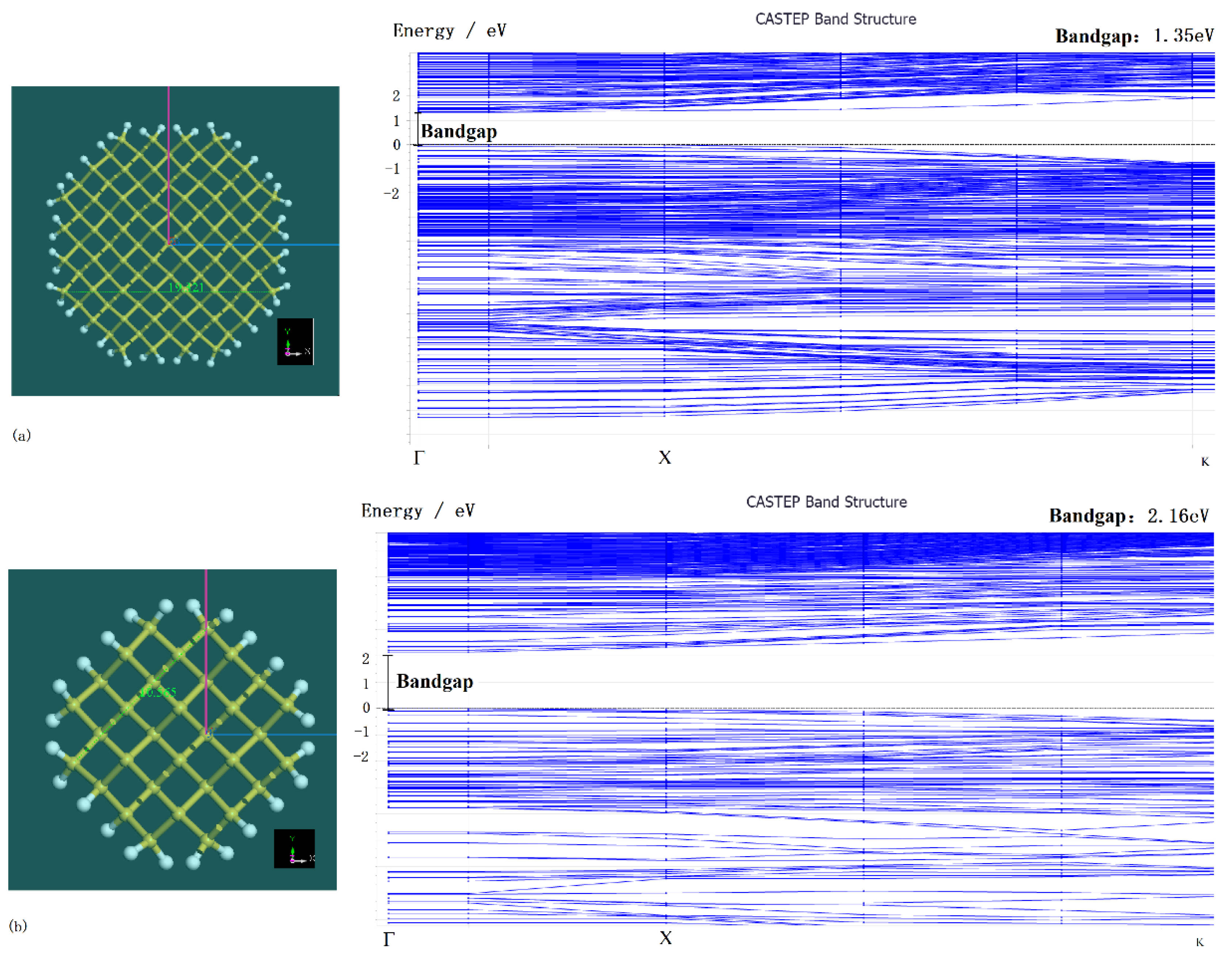
4. The Abrupt Change Effect in Bandgap Energy

In the quantum system of Si NW, we have investigated the situation near monoatomic line whose structures are shown in Figure 6, in which the radius decrease from the top picture to the bottom picture arriving monoatomic line structure. After optimum process, the convex bonding angle with 86° occurs in the monoatomic line structure for obtaining the lowest combining energy, as shown in the bottom picture and the bottom inset. Here, the symmetry of Si NW is broken from cylinder shape to monoatomic line shape.
The several structures near monoatomic line were simulated by using the CASTEP mode. Furthermore, the calculation results are exhibited in Figure 7, in which the energy band structure (a), (b) and (c) is respectively related to the top (radius: 0.55 nm), mid (radius: 0.25 nm) and bottom (radius: 0.18 nm) structure in Figure 6. Here, it is interesting that a new effect appears with disappearing of the QC effect, where the bandgap energy abruptly decreases with decreasing radius of Si NW near the monoatomic line structure, as shown in Figure 8.
The abrupt change effect in bandgap energy may be originated from transforming between two dimensions at the symmetry broken point. In the bottom picture of Figure 6, the structure near monoatomic line belongs to the fractional dimension of 1.1~1.5 in quasi-1D situation, and the bandgap will disappear to become a semi-metal as the structure transforms to the idea line shape, where new quantum phenomena and effects will appear in the process from the quasi-1D shape to the idea quantum wire.

5. Methods

5.1. Preparation of Silicon Amorphous Nanofilm

A silicon wafer (100) oriented substrate was taken on the sample stage in the combination fabrication system with pulsed laser etching (PLE) and pulsed laser deposition (PLD) devices. A pulsed Nd:YAG laser (wavelength: 1064 nm, pulse length: 60 ns FWHM, repetition rate: 1200) was used to etch lines on Si substrate in PLE process. Furthermore, then, a third harmonic of pulsed Nd:YAG laser at 355 nm was used to deposit the silicon amorphous nanofilm in PLD process.

5.2. Fabrication of Silicon NW Structure by Annealing

The silicon amorphous nanofilm was sent into the annealing furnace filled with Ar atmosphere to make annealing at 1050 ℃ for 10 min, 15 min, 20 min, 25 min and 30 min. It was discovered by using TEM analysis that the silicon quantum dots (Si QDs) began to grow and embed in the silicon amorphous nanofilm after annealing for 15 min, and then the Si QDs were connected to built the NW structure after annealing for 30 min. Here, the Si NW is embedded in the nanolayer of silicon, so the radius size of NW can be manipulated by controlling thickness of amorphous nanofilm.

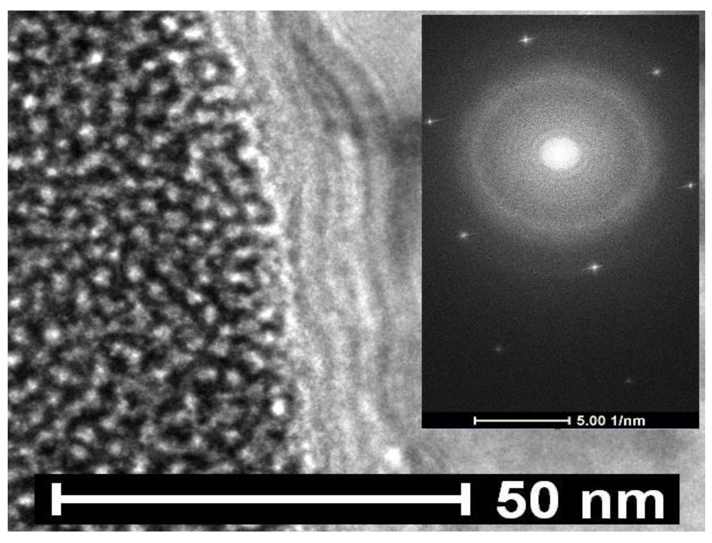
5.3. Transmission Electron Microscope (TEM) Analysis

In the TEM (JEM-2000FX) image, the Si QDs and the Si NW structures were observed in the silicon amorphous nanofilms, and the compositions were measured on the samples by using analysis in X-ray energy spectra.

6. Conclusions

In conclusion, we have explored the abrupt change effect in bandgap energy with decreasing diameter of Si NW near monoatomic line by using simulating calculation, where the QC effect disappears. In the quantum system of Si NW near monoatomic line, it has been discovered that the quantum line with special fractional structure occurs and its bandgap sharply decreases. Here, some advanced concepts with the abrupt change effect in bandgap energy have occurred and a new exploring road on nanosilicon will be opened. In the experiment, we have found the novel method with the annealing and the PLD process to fabricate the Si NW structure and to control the radius size of NW by confining cylinder space in nanolayer. These results are important for application on optic-electronic waveguide of silicon chip.

Author Contributions

Z.-M.H. is a main researcher in investigation work, who is the main researchers in experimental work, took part in the preparing process of the samples, took part in preparing Figure 4, Figure 5 and Figure 6 and made spectra measurement on the samples; S.-R.L. is a main researcher in experimental work, who took part in preparing Figure 1 and Figure 2 and took part in measurement of TEM on the samples; H.-Y.P. is a main researcher in experimental work, taking part in preparing Figure 3 and Figure 4; X.L. is a main researcher in experimental work, taking part in preparing Figure 6, Figure 7 and Figure 8; W.-Q.H. is the main writers and researchers, who wrote the main manuscript text and prepared Figure 1, Figure 2, Figure 3, Figure 4, Figure 5, Figure 6, Figure 7 and Figure 8, provided new ideas and designed investigation plan in research. All authors discussedthe results and commented on the paper. All authors have read and agreed to the published version of the manuscript.

Funding

This work was supported by the National Natural Science Foundation of China (Grant Nos. 11847084). This work was supported by Science Foundation of Guizhou (No. 20185781) and Science Foundation of Guizhou university (Nos. 2017(03), 20185781-17).

Conflicts of Interest

The authors declare no competing interests and financial interests.

References

  1. Godefroo, S.; Hayne, M.; Jivanescu, M.; Stesmans, A.; Zacharias, M.; Lebedev, O.I.; Van Tendeloo, G.; Moshchalkov, V.V. Classification and control of the origin of photoluminescence from Si nanocrystals. Nat.Nanotechnol. 2008, 3, 174–178. [Google Scholar] [CrossRef] [PubMed] [Green Version]
  2. Daldosso, N.; Luppi, M.; Ossicini, S.; Degoli, E.; Magri, R.; Dalba, G.; Fornasini, P.; Grisenti, R.; Rocca, F.; Pavesi, L.; et al. Role of the interface region on the optoelectronic properties of silicon nanocrystals embedded in SiO2. Phys.Rev. B 2003, 68, 085327. [Google Scholar] [CrossRef] [Green Version]
  3. Wolkin, M.; Jorne, J.; Fauchet, P.; Allan, G.; Delerue, C. Electronic states and luminescence in porous silicon quantum dots: The role of oxygen. Phys. Rev. Lett. 1999, 82, 197–200. [Google Scholar] [CrossRef]
  4. Pavesi, L.; Turan, R. (Eds.) Silicon Nanocrystals; Fundamentals, Synthesis, and Applications; Wiley-VCH: Roma, Italia, 2010. [Google Scholar]
  5. Koshida, N. (Ed.) Nanostructure Science and Technology: Device Applications of Silicon Nanocrystals and Nanostructures; Springer: Berlin, Germany, 2008. [Google Scholar]
  6. Qian, F.; Gradecak, S.; Li, Y.; Wen, C.Y.; Lieber, C.M. Core/Multishell Nanowire Heterostructures as Multicolor, High-Efficiency Light-Emitting Diodes. Nano Lett. 2005, 5, 2287–2291. [Google Scholar] [CrossRef] [PubMed]
  7. Abadi, R.M.I.; Saremi, M. A Resonant Tunneling Nanowire Field Effect Transistor with Physical Contractions: A Negative Differential Resistance Device for Low Power Very Large Scale Integration Applications. J. Electron. Mater. 2018, 47, 1091–1098. [Google Scholar] [CrossRef]
  8. Tomioka, K.; Motohisa, J.; Hara, S.; Hiruma, K.; Fukui, T. GaAs/AlGaAs Core Multishell Nanowire-Based Light-Emitting Diodes on Si. Nano Lett. 2010, 10, 1639–1644. [Google Scholar] [CrossRef] [PubMed]
  9. Mayer, B.; Rudolph, D.; Schnell, J.; Mork€otter, S.; Winner, J.; Treu, J.; M€uller, K.; Bracher, G.; Abstreiter, G.; Koblm€uller, G.; et al. Lasing from individual GaAs-AlGaAs core-shell nanowires up to room temperature. Nat. Commun. 2013, 4, 2931. [Google Scholar] [CrossRef] [Green Version]
  10. Saxena, D.; Mokkapati, S.; Parkinson, P.; Jiang, N.; Gao, Q.; Tan, H.H.; Jagadish, C. Optically pumped room-temperature GaAs nanowire lasers. Nat. Photonics 2013, 7, 963–968. [Google Scholar] [CrossRef]
  11. Bryllert, T.; Wernersson, L.-E.; Froberg, L.E.; Samuelson, L. Vertical High-Mobility Wrap-Gated InAs Nanowire Transistor. IEEE Electron. Device Lett. 2006, 27, 323. [Google Scholar] [CrossRef]
  12. Tomioka, K.; Yoshimura, M.; Fukui, T. A III–V nanowire channel on silicon for high-performance vertical transistors. Nature 2012, 488, 189–192. [Google Scholar] [CrossRef]
  13. Wallentin, J.; Anttu, N.; Asoli, D.; Huffman, M.; Aberg, I.; Magnusson, M.H.; Siefer, G.; Fuss-Kailuweit, P.; Dimroth, F.; Witzigmann, B.; et al. InP Nanowire Array Solar Cells Achieving 13.8% Efficiency by Exceeding the Ray Optics Limit. Science 2013, 339, 1057–1060. [Google Scholar] [CrossRef] [Green Version]
  14. Okamoto, N.; Yanagisawa, R.; Anufriev, R.; MahfuzAlam, M.; Sawano, K.; Kurosawa, M.; Nomura, M. Semiballistic thermal conduction in polycrystalline SiGe nanowires. Appl. Phys. Lett. 2019, 115, 253101. [Google Scholar] [CrossRef]
  15. M€uller, M.; Bertram, F.; Veit, P.; Loitsch, B.; Winnerl, J.; Matich, S.; Finley, J.J.; Koblm€uller, G.; Christen, J. Nanoscale mapping of carrier recombination in GaAs/AlGaAs core-multishell nanowires by cathodoluminescence imaging in a scanning transmission electron microscope. Appl. Phys. Lett. 2019, 115, 243102. [Google Scholar] [CrossRef]
  16. Han, F.; Maloth, T.; Lubineau, G.; Yaldiz, R.; Tevtia, A. Computational Investigation of the morphology, efficiency, and properties of silver nano wires networks in transparent conductive film. Sci. Rep. 2018, 8, 17494. [Google Scholar] [CrossRef]
  17. Sun, Y.; Sun, B.; He, J.; Yang, G.; Wang, C. Millimeters long super flexible Mn5Si3@SiO2 electrical nanocables applicable in harsh environments. Nat.Commun. 2020, 11, 647. [Google Scholar] [CrossRef] [PubMed]
  18. Kanzawa, Y.; Kageyama, T.; Takeoka, S.; Fujii, M.; Hayashi, S.; Yamamoto, K. Size-dependent near-infrared photoluminescence spectra of Si nanocrystals embedded in SiO2 matrix. Solid State Commun. 1997, 7, 533–537. [Google Scholar] [CrossRef]
  19. Iacona, F.; Bongiorno, C.; Spinella, C.; Boninelli, S.; Priolo, F. Formation and evolution of luminescent Si nanoclusters produced by thermal annealing of SiOx films. J. Appl. Phys. 2004, 95, 3723. [Google Scholar] [CrossRef]
  20. Zacharias, M.; Heitmann, J.; Scholz, R.; Kahler, U.; Schmidt, M.; Bläsing, J. Size-controlled highly luminescent silicon nanocrystals: A SiO/SiO2 superlattice approach. Appl. Phys. Lett. 2002, 80, 661–663. [Google Scholar] [CrossRef]
  21. Liu, C.-Y.; Holman, Z.C.; Kortshagen, U.R.L. Optimization of Si NC/P3HT hybrid solar cells. Adv. Funct. Mater. 2010, 20, 2157–2164. [Google Scholar] [CrossRef]
  22. Mangolini, L.; Thimsen, E.; Kortshagen, U. High-yield plasma synthesis of luminescent silicon nanocrystals. Nano Lett. 2005, 5, 655–659. [Google Scholar] [CrossRef]
  23. Jurbergs, D.; Rogojina, E.; Mangolini, L.; Kortshagen, U. Silicon nanocrystals with ensemble quantum yields exceeding 60%. Appl. Phys. Lett. 2006, 88, 233116. [Google Scholar] [CrossRef]
  24. Gupta, A.; Swihart, M.T.; Wiggers, H. Luminescent colloidal dispersion of silicon quantum dots from microwave plasma synthesis: Exploring the photoluminescence behavior across the visible spectrum. Adv. Funct. Mater. 2009, 19, 696–703. [Google Scholar] [CrossRef]
  25. Niesar, S.; Pereira, R.N.; Stegner, A.R.; Erhard, N.; Hoeb, M.; Baumer, A.; Wiggers, H.; Brandt, M.H.; Stutzmann, M. Low-cost post-growth treatments of crystalline silicon nanoparticles improving surface and electronic properties. Adv. Funct. Mater. 2012, 22, 1190–1198. [Google Scholar] [CrossRef]
  26. Alima, D.; Estrin, Y.; Rich, D.H.; Bar, I. The structural and optical properties of supercontinuum emitting Si nanocrystals prepared by laser ablation in water. J. Appl. Phys. 2012, 112, 114312. [Google Scholar] [CrossRef] [Green Version]
  27. Crouch, C.H.; Carey, J.E.; Warrender, J.M.; Aziz, M.J.; Mazur, E.; Génin, F.Y. Comparision of structure and properties of femtosecond and nanosecond laser-structured silicon. Appl. Phys. Lett. 2004, 84, 1850–1852. [Google Scholar] [CrossRef]
  28. Huang, W.Q.; Liu, S.R.; Huang, Z.M.; Dong, T.G.; Wang, G.; Qin, C.J. Magic electron affection in preparation process of silicon nanocrystal. Sci. Rep. 2015, 4, 9932. [Google Scholar] [CrossRef] [PubMed] [Green Version]
  29. Huang, W.Q.; Wu, X.K.; Liu, S.R.; Qin, C.J. Curved surface effect and manipulation of electronic states in nanosilicon. Sci. Rep. 2017, 7, 17974. [Google Scholar] [CrossRef]
Figure 1. TEM Image of Si NW conformed in the growth process with connecting nanoparticles on silicon amorphous nanofilm.
Crystals 10 00340 g001
Figure 2. TEM Image of Si NW confined in the nanolayer on amorphous film, where the inset shows the electronic diffraction pattern of the Si NW structure.
Crystals 10 00340 g002
Figure 3. Structure model of Si NW in simulation, in which the top picture shows cross-section structure and the bottom picture shows the lateral view of Si NW structure.
Crystals 10 00340 g003
Figure 4. Energy change of bandgap with various radius of Si NW in simulation. (a)Si NW model with diameter of 2 nm and its energy band structure calculated (b) Si NW model with diameter of 1nm and its energy band structure calculated.
Crystals 10 00340 g004
Figure 5. Change curve of bandgap energy with various diameter of Si NW, in which the black curve describes the simulating result and the red curve is fit one.
Crystals 10 00340 g005
Figure 6. Structure change near monoatomic line, in which the top picture shows Si NW structure with radius of 0.55nm, the mid picture shows Si NW structure with radius of 0.25 nm, and the bottom picture exhibits monoatomic line structure of silicon in which the convex bonding angle with 86° occurs at lowest combining energy as shown in the bottom inset.
Crystals 10 00340 g006
Figure 7. The energy band constructions respectively related to the top picture structure (a), the mid picture structure (b), and the bottom picture structure (c) in Figure 6.
Crystals 10 00340 g007
Figure 8. Energy change of bandgap with decreasing diameter of Si NW near monoatomic line.
Crystals 10 00340 g008

