Abstract
A technique for direct study of the distribution of the applied voltage within a quantum cascade laser (QCL) has been developed. The detailed profile of the potential in the laser claddings and laser core region has been obtained by gradient scanning Kelvin probe force microscopy (KPFM) across the cleaved facets for two mid-infrared quantum cascade laser structures. An InGaAs/InAlAs quantum cascade device with InP claddings demonstrates a linear potential distribution across the laser core region with constant voltage drop across the doped claddings. By contrast, a GaAs/AlGaAs device with AlInP claddings has very uneven potential distribution with more than half of the voltage falling across the claddings and interfaces around the laser core, greatly increasing the overall voltage value necessary to achieve the lasing threshold. Thus, KPFM can be used to highlight design and fabrication flaws of QCLs.
1. Introduction
Metalorganic vapour phase epitaxy (MOVPE) of quantum cascade lasers (QCLs) [1,2] is a very demanding process. The interface abruptness, intentional and unintentional doping, layer thicknesses, and material compositions may critically affect the performance of any conventional laser diodes. Taking into account that thicknesses of individual layers in a QCL active region can be just a few atomic monolayers and the total number of individual layers is typically many hundreds, the control of the above parameters in QCLs is even more difficult. Various experimental techniques are used to assess the structural, electrical, optical and thermal properties of the as-grown material and fabricated devices, e.g., [3,4,5,6,7,8,9,10,11,12,13,14,15,16,17,18,19] in order to help to optimize the QCL design and related epitaxial growth technologies. In this paper, we present a technique for direct, high-spatial-resolution measurements of the voltage distribution across all the parts of QCL structures. The technique is based on Kelvin probe force microscopy (KPFM), which is widely used to study other electrically driven semiconductor devices [20,21,22,23].
It is usually assumed that the whole voltage that is applied to a QCL device is dropped only across the laser core, with negligible contribution from other parts such as top and bottom claddings or contact and spacer layers. Despite some agreement between the operating and predicted voltage values for working QCLs, there is high degree of uncertainty on how exactly the electric field is distributed across different layers of QCLs. In this study, QCL devices based on InP and GaAs substrates have been tested, revealing examples of both almost ideal voltage distribution and the existence of the areas of excessive parasitic voltage drop.
2. Materials and Methods
GaAs/AlGaAs on GaAs and InGaAs/InAlAs on InP QCL structures were grown by MOVPE in a horizontal flow reactor. Trimethylaluminium, trimethylgallium, trimethylindium, arsine and phosphine were used as the precursors of the group III and V atoms. Disilane was used for n-type doping. Hydrogen was used as a carrier gas. The total reactor pressure was 150 Torr. The orientation of the epitaxial surface of the InP substrates was (100) on-axis. The orientation of the GaAs substrates was (100), with a miscut angle of 10o towards <111> A in order to suppress the CuPt-type ordering in Al(Ga)InP [24,25]. All substrates were n-type doped with n > 1018 cm−3.
λ ≈ 9.7 µm GaAs/AlGaAs QCL wafer (sample MR2790) was grown with a 1 µm thick GaAs (n = 6 × 1018 cm−3) buffer layer. A 3.04 µm thick GaAs/Al0.45Ga0.55As laser core with 55 cascade periods and average doping of n = 7 × 1016 cm−3 is surrounded by a 0.2 µm thick top and bottom GaAs (n = 5 × 1016 cm−3) spacer layers and 3 µm thick top and bottom In0.47Al0.53P (n = 5 × 1016 cm−3) claddings. Finally, the structure was capped with a 1 µm thick GaAs (n = 6 × 1018 cm−3) top contact layer. The details of the laser core of this structure can be found in [26].
The design of the active region of the λ ≈ 5.7 µm InGaAs/InAlAs strain-compensated QCL wafer (sample MR2449) is very similar to that presented in [27]. The structure has a 2.125 µm thick In0.6Ga0.4As/In0.42Al0.58As laser core with 35 cascade periods and average doping of n = 2 × 1016 cm−3 surrounded by 0.3 µm thick In0.53Ga0.47As (n = 6 × 1016 cm−3) top and bottom spacer layers and 2.3 µm thick InP (n = 1 × 1017 cm−3) top and bottom claddings. This structure has a 0.8 µm thick highly doped (n = 7 × 1018 cm−3) InP top contact layer.
Fully processed 3 mm long lasers from both wafers operate above room temperature with a pulsed (50 ns pulse width at 5 kHz repetition rate) threshold current density of 4.4 kA/cm2 and 2.5 kA/cm2 at 300 K for the GaAs- and InP-based QCLs, correspondingly. The current–voltage (IV) characteristics for both QCL devices are presented in Figure 1. The theoretical operating voltage (in Volts) at the threshold, assuming that the total voltage drops only across the laser core, can be estimated as Uth = N(Eem + Einj)/e, where N is the number of cascade periods, Eem is the laser emission energy in eV, e is the electron charge and Einj is the energy “width” of the miniband in the injector part of the cascade period at the alignment—often called the voltage defect. The theoretical values for the voltage at the laser threshold are 14.8 V and 10.6 V for MR2790 and MR2449, correspondingly. For the MR2449 device, the observed voltage is very similar to the predicted one, while the MR2790 laser requires a much higher voltage (27 V) to achieve lasing. It was suggested [26] that the high potential barrier in the conduction band offset (up to 0.3 eV) on the GaAs/InAlP interfaces can lead to an increased resistance and operating voltage. In an attempt to minimise this effect, a transitional layer between GaAs and InAlP materials is incorporated into the MR2790 QCL structure. The layer provides a step-wise, less abrupt change in the conduction band profile and consists of 25 nm of In0.49Ga0.51P followed by 15 nm of In0.49(Ga0.5Al0.5)0.51P in the direction from GaAs to InAlP, while the layer sequence is reversed for the direction from InAlP to GaAs. However, despite the introduction of this transitional layer, the operating voltage appears to still be higher than the predicted one.
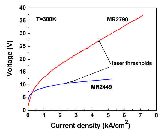
Figure 1.
Current–voltage characteristics for 3 mm long λ ≈ 9.7 µm GaAs/AlGaAs QCL (MR2790) and λ ≈ 5.7 µm InGaAs/InAlAs QCL (MR2449) with a pulsed threshold current density of 4.4 kA/cm2 and 2.5 kA/cm2 at 300 K, respectively.
The measurements of voltage distribution across the cleaved QCL facets were carried out using an NT-MDT NTegra Aura atomic force microscopy (AFM) setup in the regime of amplitude modulated gradient scanning Kelvin probe force microscopy (AM-GKPFM) [28,29,30]. The microscopy head has a track system based on a λ = 1.3 µm infrared laser. The typical spatial resolution for the measured potential distributions and topography maps is better than 100 nm. Measurements were carried out using uncoated highly n-doped silicon NSG11 cantilevers, AM-GKPFM operated in two-pass lift mode; the amplitude of cantilever mechanical oscillations was 40 nm; lift 30 nm; cantilever bias voltage amplitude was 0.5 V, see [29] for detailed description of measurement method. The QCL chips were cleaved at atmospheric pressure outside the vacuum chamber, soldered epi-side up on copper submounts and then put under vacuum. The negative cw bias, relative to the earthed submount, was applied to the top of the laser ridge. The measurements were performed at room temperature and at reduced pressure (~0.1 mBar). The size of the cleaved ridge devices used in the KPFM experiments is 0.27 mm long and 20 µm wide for wafer MR2790, and 2 mm long and 20 µm wide for wafer MR2449.
3. Results and Discussion
The topography map of the cleaved facet measured in the tapping mode of AFM [31] is obtained along with the voltage dependence. This helps to eliminate the possible features on voltage distribution graphs associated with unevenness or foreign particles that have appeared on the cleaved surface. The typical topography map of the part of the cleaved facet for the device from MR2790 is presented in Figure 2. The highest roughness in the cleaved surface flatness does not exceed a few nm. The GaAs/AlGaAs laser core is clearly visible—positioned approximately between the 3 and 6 µm marks on the horizontal scale. On both sides around the laser core there are darker layers, which are about 200 to 250 nm wide, corresponding to the GaAs spacer layers. The white spots are probably related to contaminating foreign particles on the facet surface. The larger spots appear along the interface between the core region and the spacers, while the smaller ones are distributed across the bottom and top AlInP claddings. The surface of the core region part is clear from such particles. Such a distribution is not yet fully understood; however, this can also be of a chemical nature, for example, selective oxidation of clusters formed in AllnP material.
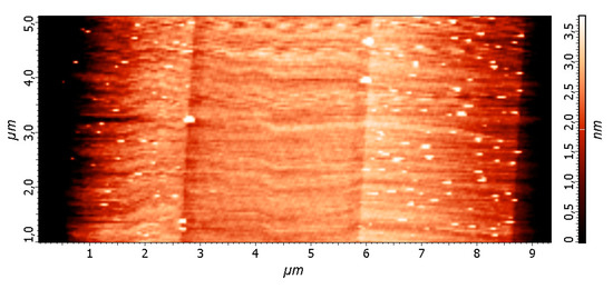
Figure 2.
Topographic map for the cleaved facet of the GaAs/AlGaAs quantum cascade laser obtained in the tapping regime of AFM. The laser core is between ~3 and ~6 µm on the horizontal scale with 0.2 µm thick GaAs spacers and 3 µm wide AlInP claddings surrounding it on both sides. The GaAs substrate is on the right.
The scanning time for one line in the KPFM regime is just above 3 minutes, where half of this is spent for the actual measurement and another half for the back sweep. The contact potential difference profile under zero bias (CPD(0)) is recorded first. This CPD(0) value is then subtracted from the CPD(V) values measured at non-zero applied bias. The subtraction of CPD(0) values recorded at zero bias from all CPD(V) curves measured subsequently is used to partly eliminate the contribution from the static surface effects. However, if the charging/discharging of surface states have a relatively long-term dependence, then these effects should be studied separately and in much more detail. For each given applied voltage, just one CPD(V) scan was used. The voltage and the current values in these experiments are controlled with precision greater than 1 mV and 0.1 mA, correspondingly.
The ΔCPD = CPD(V) − CPD(0) profiles for the device from wafer MR2790 are presented in Figure 3 for the bias values up to 7 V (compare with IV curve for this laser in Figure 1). These ΔCPD scans have been taken at the position on the facet close to the top of the topographic image in Figure 2. The relative layout of the AlInP claddings, GaAs layers and the laser core in this figure is given as a reference. It should be noted that for the maximum applied bias used in these experiments, the detected shift of the sample mounted on the copper holder due to thermal expansion was around 6 µm (the temperature increased up to 30 K). Because of this temperature shift, all ΔCPD scans have been adjusted (with accuracy better than 0.1 µm) to be at the same position on the sample facet.
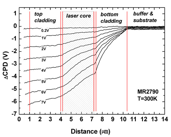
Figure 3.
Contact potential difference profiles for the GaAs-based QCL with AlInP claddings measured on the cleaved laser facet by KPFM technique for various applied bias.
The applied voltage for the MR2790 device does not drop only across epitaxial layers. Up to 5% of the total bias has been found to fall outside of them, probably on the electrical contacts or the GaAs substrate. Almost half of the total voltage drops on the bottom AlInP cladding, while the drop on the top AlInP cladding is less; however, it is still excessive. Note, that top and bottom claddings were designed and specified during the growth process to have the same composition and doping level; however, KPFM measurements show that the voltage drop across the top and bottom claddings is different. This can be caused by the different concentration of localized defects and provides a new topic for future investigation. The voltage distribution across the laser core is not precisely linear, resulting in the cascade periods having different levels of alignment at any given bias. We note that some unevenness in the surface topography might contribute to the appearance of a slightly non-linear voltage distribution in the laser core. However, it is unlikely as the position of the “inflection” point on this dependence is shifting with bias increase from being closer to the top cladding towards the bottom cladding.
After the ΔCPD scan was completed under the applied bias of 7 V, the voltage was decreased back to 4 V. Surprisingly, the re-measured potential profile does not exactly follow the one obtained for the same 4 V bias but from when the bias value had increased from zero volts (see Figure 4). Such a hysteresis might indicate that the charge accumulated near the GaAs/AlInP interface at higher voltage and was still not dissipated when the voltage had dropped. Another indication of a slow discharge process in the area of the bottom cladding is the ΔCPD dependences (see Figure 4) taken at zero bias straightaway after the main series of ΔCPD measurements had been finished. The ΔCPD graphs have been obtained in 3, 6 and 9 minutes after the bias was switched-off. Such extremely long relaxation time is very unlikely to be defined only by the processes happening in the volume of the semiconductor structure but also by kinetics of the surface states. On the other hand, deep traps for the electrons which might be formed in the energy gap of the Al-rich AlInP claddings and high conduction band discontinuity on GaAs/AlInP interfaces might contribute to such slow-discharging surface states. The charge accumulation is observed mainly in the bottom cladding and closer to the interface with the core. This behaviour can be explained partly by the different conditions on the interfaces between GaAs and AlInP in different parts of the epitaxial structure. It should not be an obstacle for the electrons to fall from the higher conduction band of AlInP when they move through AlInP/GaAs interfaces. To move through GaAs/AlInP interfaces is much harder even with the incorporated transitional layer. The higher doping level on the interface between the top contact GaAs layer and the top AlInP cladding should help to reduce the band offset by “levelling” the bottoms of their conduction bands. However, the conduction band profile on the GaAs/AlInP interface between the laser core and the bottom cladding may not be smooth enough because the doping level in this area is intentionally kept low to reduce possible free-carrier absorption, which can result in higher waveguide losses. The actual doping level in the AlInP claddings, which might end up being lower than intended due to possible formation of the deep traps, may also be the reason for an excessive voltage drop across the claddings. We believe that more growth runs and further optimization of the structural design are needed to reduce the voltage drop in the GaAs-based QCLs with AlInP claddings.
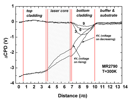
Figure 4.
Contact potential difference profiles for the GaAs-based QCL with AlInP claddings measured on the cleaved laser facet by the KPFM technique. The observed hysteresis (the voltage was increased from 0 to 4 V for the first measurement and the voltage was decreased from 7 to 4 V for the second one) and a very slow time dependence (measured in 3, 6 and 9 minutes) after switch-off might indicate the existence of charge that has accumulated around the bottom AlInP cladding.
The observed voltage distribution across the MR2449 device is much more predictable (see Figure 5) compared with the MR2790 device. Almost all the applied voltage is dropped linearly across the laser core, demonstrating equal level alignment for all cascade periods. There is negligible voltage drop across the cladding and spacer layers. The difference between the predicted (10.6 V) and the observed (10.8 V) voltage at the threshold is minimal and depends on the slight variation in the level alignment and band bending due to charge redistribution in the active and injector regions, which was not included in the voltage calculations. Neither hysteresis nor slow time evolution of ΔCPD dependences have been observed for the MR2449 device.
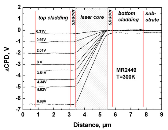
Figure 5.
Contact potential difference profiles for the InP-based QCL measured on the cleaved laser facet by KPFM technique for various applied bias.
4. Conclusions
We have presented a technique for the detailed study of the spatial distribution of the applied voltage across the epitaxial structure of mid-infrared QCLs. The GaAs-based QCL with AlInP waveguides demonstrates an uneven potential drop across its laser core and very high parasitic voltage drops across the cladding layers. The developed method can be very valuable for the optimization of the QCL design as well as the epitaxial growth technology of QCLs. The detailed knowledge of the voltage distribution might be particularly important for the broadband QCLs, where all sections in the laser core designed for different wavelengths should achieve optimum alignment at the same applied bias values.
Author Contributions
All authors contributed to conceiving the experiment. K.L. and V.E. performed the Kelvin probe measurements. A.K. contributed to the design of QCLs, engineered the epitaxial process and grew the QCL wafers. D.R. designed the QCL structures and measured the laser performance. All authors contributed to the data analysis and discussion. K.L. and D.R. drafted the manuscript. All authors have read and agreed to the published version of the manuscript.
Funding
This work was supported by the EPSRC UK, by the European Union Marie Curie IAPP project “QUANTATEC”, K.L. was supported by Russian Science Foundation (Project 19-19-00683, development of KPFM measurement methodology). A considerable amount of the research presented in this paper was carried out outside of the normal working hours.
Acknowledgments
A.K. would like to thank David Morris, Chief Research Technician, for his assistance in the MOVPE lab.
Conflicts of Interest
The authors declare no conflict of interest. The funders had no role in the design of the study; in the collection, analyses, or interpretation of data; in the writing of the manuscript, or in the decision to publish the results.
References
- Green, R.P.; Krysa, A.B.; Roberts, J.S.; Wilson, L.R.; Cockburn, J.W.; Revin, D.G.; Zibik, E.; Ng, W.H. Room-temperature operation of InGaAs/AlInAs quantum cascade lasers grown by metalorganic vapor phase epitaxy. Appl. Phys. Lett. 2003, 83, 1921. [Google Scholar] [CrossRef]
- Krysa, A.B.; Roberts, J.; Green, R.; Wilson, L.; Page, H.; García, M.; Cockburn, J. MOVPE-grown quantum cascade lasers operating at ∼9 μm wavelength. J. Cryst. Growth 2004, 272, 682–685. [Google Scholar] [CrossRef]
- Spagnolo, V.; Troccoli, M.; Scamarcio, G.; Gmachl, C.; Capasso, F.; Tredicucci, A.; Sergent, A.M.; Hutchinson, A.L.; Sivco, D.L.; Cho, A.Y. Temperature profile of GaInAs/AlInAs/InP quantum cascade-laser facets measured by microprobe photoluminescence. Appl. Phys. Lett. 2001, 78, 2095–2097. [Google Scholar] [CrossRef]
- Offermans, P.; Koenraad, P.M.; Wolter, J.H.; Beck, M.; Aellen, T.; Faist, J. Digital alloy interface grading of an InAlAs/InGaAs quantum cascade laser structure studied by cross-sectional scanning tunneling microscopy. Appl. Phys. Lett. 2003, 83, 4131–4133. [Google Scholar] [CrossRef]
- Revin, D.G.; Wilson, L.R.; Cockburn, J.W.; Krysa, A.B.; Roberts, J.S.; Airey, R.J. Intersubband spectroscopy of quantum cascade lasers under operating conditions. Appl. Phys. Lett. 2006, 88, 131105. [Google Scholar] [CrossRef]
- Yu, N.; Diehl, L.; Cubukcu, E.; Pflügl, C.; Bour, D.; Corzine, S.; Zhu, J.; Höfler, G.; Crozier, K.; Capasso, F. Near-field imaging of quantum cascade laser transverse modes. Opt. Express 2007, 15, 13227–13235. [Google Scholar] [CrossRef]
- Kuehn, W.; Parz, W.; Gaal, P.; Reimann, K.; Woerner, M.; Elsaesser, T.; Muüller, T.; Darmo, J.; Unterrainer, K.; Austerer, M.; et al. Ultrafast phase-resolved pump-probe measurements on a quantum cascade laser. Appl. Phys. Lett. 2008, 93, 151106. [Google Scholar] [CrossRef]
- Wang, C.; Goyal, A.; Huang, R.; Donnelly, J.; Calawa, D.; Turner, G.; Sanchez-Rubio, A.; Hsu, A.; Hu, Q.; Williams, B. Strain-compensated GaInAs/AlInAs/InP quantum cascade laser materials. J. Cryst. Growth 2010, 312, 1157–1164. [Google Scholar] [CrossRef]
- Grasse, C.; Katz, S.; Böhm, G.; Vizbaras, A.; Meyer, R.; Amann, M.-C. Evaluation of injectorless quantum cascade lasers by combining XRD- and laser-characterisation. J. Cryst. Growth 2011, 323, 480–483. [Google Scholar] [CrossRef][Green Version]
- Pierściński, K.; Pierścińska, D.; Iwinska, M.; Kosiel, K.; Szerling, A.; Karbownik, P.; Bugajski, M. Investigation of thermal properties of mid-infrared AlGaAs/GaAs quantum cascade lasers. J. Appl. Phys. 2012, 112, 043112. [Google Scholar] [CrossRef]
- Friedli, P.; Sigg, H.; Wittmann, A.; Terazzi, R.; Beck, M.; Kolek, A.; Faist, J. Synchrotron infrared transmission spectroscopy of a quantum cascade laser correlated to gain models. Appl. Phys. Lett. 2013, 102, 12112. [Google Scholar] [CrossRef]
- Enobio, E.C.I.; Ohtani, K.; Ohno, Y.; Ohno, H. Detection and measurement of electroreflectance on quantum cascade laser device using Fourier transform infrared microscope. Appl. Phys. Lett. 2013, 103, 231106. [Google Scholar] [CrossRef]
- Kubacka-Traczyk, J.; Sankowska, I.; Seeck, O.; Kosiel, K.; Bugajski, M. High-resolution X-ray characterization of mid-IR Al0.45Ga0.55As/GaAs Quantum Cascade Laser structures. Thin Solid Films 2014, 564, 339–344. [Google Scholar] [CrossRef]
- Michalowski, P.; Gutowski, P.; Pierścińska, D.; Pierściński, K.; Bugajski, M.; Strupiński, W. Characterization of the superlattice region of a quantum cascade laser by secondary ion mass spectrometry. Nanoscale 2017, 9, 17571–17575. [Google Scholar] [CrossRef] [PubMed]
- Walther, T.; Krysa, A.B. Transmission electron microscopy of AlGaAs/GaAs quantum cascade laser structures. J. Microsc. 2017, 268, 298–304. [Google Scholar] [CrossRef]
- Rajeev, A.; Chen, W.; Kirch, J.; Babcock, S.E.; Kuech, T.F.; Earles, T.; Mawst, L. Interfacial Mixing Analysis for Strained Layer Superlattices by Atom Probe Tomography. Crystals 2018, 8, 437. [Google Scholar] [CrossRef]
- Lü, X.; Luna, E.; Schrottke, L.; Biermann, K.; Grahn, H. Determination of the interface parameter in terahertz quantum-cascade laser structures based on transmission electron microscopy. Appl. Phys. Lett. 2018, 113, 172101. [Google Scholar] [CrossRef]
- Becher, N.; Farzaneh, M.; Knipfer, B.; Sigler, C.A.; Kirch, J.; Boyle, C.; Botez, D.; Mawst, L.; Lindberg, D.F.; Earles, T. Thermal imaging of buried heterostructure quantum cascade lasers (QCLs) and QCL arrays using CCD-based thermoreflectance microscopy. J. Appl. Phys. 2019, 125, 033102. [Google Scholar] [CrossRef]
- Khabibullin, R.; Shchavruk, N.; Ponomarev, D.; Ushakov, D.; Afonenko, A.; Maremyanin, K.; Volkov, O.; Pavlovskiy, V.; Dubinov, A. The operation of THz quantum cascade laser in the region of negative differential resistance. Opto-Electron. Rev. 2019, 27, 329–333. [Google Scholar] [CrossRef]
- Weber, S.; Hermes, I.; Turren-Cruz, S.-H.; Gort, C.; Bergmann, V.W.; Gilson, L.; Hagfeldt, A.; Graetzel, M.; Tress, W.; Berger, R.; et al. How the formation of interfacial charge causes hysteresis in perovskite solar cells. Energy Environ. Sci. 2018, 11, 2404–2413. [Google Scholar] [CrossRef]
- Chen, C.; Song, Z.; Xiao, C.; Zhao, D.; Shrestha, N.; Li, C.; Yang, G.; Yao, F.; Zheng, X.; Ellingson, R.J.; et al. Achieving a high open-circuit voltage in inverted wide-bandgap perovskite solar cells with a graded perovskite homojunction. Nano Energy 2019, 61, 141–147. [Google Scholar] [CrossRef]
- Utama, M.I.B.; Kleemann, H.; Zhao, W.; Ong, C.S.; Da Jornada, F.H.; Qiu, D.Y.; Cai, H.; Li, H.; Kou, R.; Zhao, S.; et al. A dielectric-defined lateral heterojunction in a monolayer semiconductor. Nat. Electron. 2019, 2, 60–65. [Google Scholar] [CrossRef]
- Ranjan, R.; Prakash, A.; Singh, A.; Singh, A.; Garg, A.; Gupta, R. Effect of tantalum doping in a TiO2 compact layer on the performance of planar spiro-OMeTAD free perovskite solar cells. J. Mater. Chem. A 2018, 6, 1037–1047. [Google Scholar] [CrossRef]
- Suzuki, T.; Gomyo, A.; Iijima, S. Strong ordering in GaInP alloy semiconductors; Formation mechanism for the ordered phase. J. Cryst. Growth 1988, 93, 396–405. [Google Scholar] [CrossRef]
- Minagawa, S.; Kondow, M. Dependence of photoluminescence peak energy of MOVPE-grown AlGaInP on substrate orientation. Electron. Lett. 1989, 25, 758. [Google Scholar] [CrossRef]
- Atkins, C.; Krysa, A.B.; Revin, D.; Kennedy, K.; Commin, J.; Cockburn, J. Low threshold room temperature GaAs/AlGaAs quantum cascade laser with InAlP waveguide. Electron. Lett. 2011, 47, 1193. [Google Scholar] [CrossRef]
- Zasavitskii, I.I.; Kovbasa, N.Y.; Raspopov, N.A.; Lobintsov, A.V.; Kurnyavko, Y.V.; Gorlachuk, P.V.; Krysa, A.B.; Revin, D.G. A GaInAs/AlInAs quantum cascade laser with an emission wavelength of 5.6 μm. Quantum Electron. 2018, 48, 472–475. [Google Scholar] [CrossRef]
- Melitz, W.; Shen, J.; Kummel, A.C.; Lee, S. Kelvin probe force microscopy and its application. Surf. Sci. Rep. 2011, 66, 1–27. [Google Scholar] [CrossRef]
- Ladutenko, K.S.; Ankudinov, A.V.; Evtikhiev, V.P. On the accuracy of quantitative measurements of the local surface potential. Tech. Phys. Lett. 2010, 36, 228–231. [Google Scholar] [CrossRef]
- Girard, P.; Ramonda, M.; Saluel, D. Electrical contrast observations and voltage measurements by Kelvin probe force gradient microscopy. J. Vac. Sci. Technol. B Microelectron. Nanometer Struct. 2002, 20, 1348. [Google Scholar] [CrossRef]
- Zhong, Q.; Inniss, D.; Kjoller, K.; Elings, V. Fractured polymer/silica fiber surface studied by tapping mode atomic force microscopy. Surf. Sci. Lett. 1993, 290, L688–L692. [Google Scholar]
© 2020 by the authors. Licensee MDPI, Basel, Switzerland. This article is an open access article distributed under the terms and conditions of the Creative Commons Attribution (CC BY) license (http://creativecommons.org/licenses/by/4.0/).