Abstract
As a core component of photovoltaic power generation systems, insulated gate bipolar transistor (IGBT) modules continually suffer from severe temperature swings due to complex operation conditions and various environmental conditions, resulting in fatigue failure. The junction temperature prediction guarantees that the IGBT module operates within the safety threshold. The thermal equivalent circuit model is a common approach to predicting junction temperature. However, the model parameters are easily affected by the solder aging. An accurate temperature prediction by the model is impossible during service. This paper proposes an improved thermal equivalent circuit model that can remove the effect of solder aging. Firstly, the solder aging process is monitored in real-time based on the case temperatures. Secondly, the model parameters are corrected by the thermal impedance from chip to baseplate based on the linear thermal characteristic. The simulation and experimental results show that the proposed model can reduce the temperature prediction error by more than 90% under the same aging condition. The proposed method only depends on the case temperatures to correct the model parameters, which is more economical. In addition, the experimental and simulation analysis in this work can help students of power electronics courses have an in-depth knowledge of power devices’ mechanical structure, heat dissipation principles, temperature distribution, junction temperature monitoring, and so on.
1. Introduction
Photovoltaic power generation technology has taken a significant leap in the past several decades, due to advances in materials, power converters, and energy storage. Photovoltaic power generation systems usually exist in arid natural environments such as deserts. Various components easily break due to the complex operation environments. The photovoltaic power generation industry is cost-sensitive to the market, and frequent failures may make photovoltaic power generation lose competitiveness [1]. Therefore, new technologies are necessary to improve the performance and reliability of the system during operation. Power converters consist of IGBT modules, which are one of the most vulnerable components in the system. Due to harsh environments and unpredictable mission profiles, IGBT modules are often subjected to enormous and uncertain temperature fluctuations, leading to degradation of electrical performance and even device damage. Studies show that temperature caused more than 60% of device failures [2]. In addition, the probability of device failure doubles for every 10 °C increase in temperature [3]. Therefore, accurately predicting the temperature of the IGBT modules and making the modules run below the safety threshold is a vital means to improve the reliable performance of the device, and it is also a guarantee for the development of the photovoltaic power generation industry.
Real-time junction temperature prediction is the key to extending the reliability of the IGBT modules. The thermal equivalent circuit model is a frequently used temperature prediction approach for long-term load scenarios because of its simplicity and high efficiency. In the past few years, many researchers have improved the performance of thermal equivalent circuit models in many aspects, such as thermal coupling between different layers or adjacent chips, thermal boundary states, temperature-dependent materials, and computational efficiency [4,5,6,7,8,9]. For instance, a lot of research in the literature uses the finite-element analysis method for detailed three-dimensional temperature information to solve the issue of thermal coupling and thermal boundary conditions. In addition, much work has been carried out on computationally efficient thermal behavior modeling for power semiconductor devices when the devices are healthy [10,11,12,13]. A temperature characteristics-based dynamic model is able to remove the effect of temperature on material properties [14,15,16,17]. Scognamillo et al. proposed an innovative technique that allows the experimental extraction of the junction-to-ambient thermal impedance () of power devices operating in their application environment [18]. The above-proposed methods improve the performance of thermal equivalent circuit models in different applications.
Unfortunately, the aforementioned means ignore the effect of solder aging on the model parameters. The solder aging changes the thermal path inside the IGBT modules, resulting in a mismatch between the model parameters and the device’s mechanical structure [19,20,21]. The junction temperature prediction based on the model may be much lower than the real chip temperature, resulting in an optimistic evaluation of the module’s operation conditions. Finally, the aging process of the IGBT module is accelerated. Based on the above analysis, a thermal equivalent circuit model that has the ability to remove the effect of solder aging is more necessary. In [22,23], model parameters were revised by the variations of thermal impedance due to solder aging. However, these methods still have some limitations: (a) Only the thermal resistance is corrected, and the heat capacity is neglected, due to the lack of research on the influence mechanism of solder aging on model parameters, resulting in the prediction accuracy of junction temperature cannot be completely restored. (b) The calculation of thermal impedance depends on the measurement of chip junction temperature. However, the temperature-sensitive electrical parameters (TSEP) including collector–emitter on-state voltage and gate-source voltage are susceptible to the bond wires and gate oxide degradation [24,25,26]. These limitations make it impossible to apply the model to high-precision situations. Therefore, there are still some challenges in correcting the model parameters completely and estimating the thermal impedance economically.
Motivated by the above analysis, this paper proposes an improved thermal equivalent circuit model that can remove the influence of solder aging on temperature prediction. This work includes two aspects: (a) the solder aging process is real-time monitored based on case temperatures and the thermal impedance variations are estimated according to the case temperatures; (b) model parameters consisting of thermal resistance and thermal capacitance are corrected based on linear thermal characteristics. The model parameters are corrected timely to obtain the device’s accurate junction temperature through the above two stages. Finally, the reliability of power converters under various operational states is improved.
Power electronics is a theoretical course that introduces the basic principles, analytical methods, and typical applications of power electronics technology, which is the basis of professional knowledge in electrical disciplines. Power electronics contains the characteristics and use methods of semiconductor power devices, and the working principles and analysis methods of three-phase rectifier, chopper, inverter, and frequency conversion circuits. Structural characteristics and thermal reliability monitoring of semiconductor power devices are hardly involved. As the core component of a photovoltaic power generation system, the thermal reliability of the semiconductor power device affects the reliability of the whole power generation system. The thermal failure principle of semiconductor power devices and how to carry out thermal management are significant methods to improve students’ understanding of power devices. This paper introduces the temperature monitoring method and the thermal failure principle of the power device. At the same time, the finite element analysis method and accelerated aging test method are introduced in the simulation and experiment section. Students can have a more comprehensive understanding of the mechanical structure, failure principle, heat dissipation mechanism, temperature monitoring, and so on.
The remainder of this article is as follows. In Section 2, the monitoring algorithm of solder aging in real-time and the correction theory of model parameters are introduced. In Section 3 and Section 4, the finite-element analysis and experimental analysis are employed to validate the effectiveness of the proposed method, respectively.
2. Method
2.1. Monitoring of Solder Aging in Real-Time
The chip is considered the heat source of the IGBT module. The heat is generally generated on the upper surface of the chip and transferred from the chip to the baseplate through various layers with different materials. A great amount of heat flow spreads down with an angle of 45°, resulting in the baseplate containing a higher temperature distribution than the chip, as shown in Figure 1.
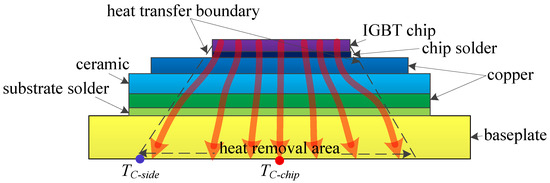
Figure 1.
The thermal path of a healthy IGBT module (the arrows represent the heat flow).
The thermal impedance from chip to baseplate is a commonly used parameter to characterize the property of the thermal path. The formula of is as follows.
where P denotes the device’s power loss, is the junction temperature of the chip, and is the case temperature at the center of the baseplate.
A smaller value of results in faster heat diffusion. Solder aging originates from the layer’s side region and extends to the central region, as shown in Figure 2. Solder aging indicates that cracks or voids are generated in the solder layer. The heat transfer channel becomes narrower due to the cracks and voids. Most heat can only be transferred to the baseplate by the central non-crack area, resulting in heat accumulating inside the module. The final expression is the increase of value. Because of this, is able to monitor solder aging timely. However, the estimation depends on the junction temperature . The thermal equivalent circuit model cannot acquire the accurate junction temperature as the solder aging exists. As a result, it cannot accurately calculate by the model. The temperature-sensitive electrical parameters (TSEPs) method is another way to measure the junction temperature. However, the TSEPs method requires a high-precision circuit that is expensive. In addition, the TSEPs are susceptible to bond wires and gate oxide degradation. Therefore, a cost-effective and reliable monitoring method for solder aging is urgently needed.

Figure 2.
The thermal path of an aged IGBT module (the arrows represent the heat flow).
The baseplate’s thermal diffusion property can be characterized by which is the thermal impedance from the baseplate to the ambient. The formula of is as follows.
where P is the device’s power loss, is the case temperature of the baseplate, and is the ambient temperature.
Since the temperature distribution of the baseplate is nonuniform, the thermal diffusion properties of different regions are distinct. That is to say, the value of is various. Most heat generated in the chip transfers to the baseplate along the optimal path, i.e., the vertical direction. Therefore, the central temperature of the baseplate is higher than the rest. Solder aging generally originates from the side area and extends to the central area. As a result, the heat accumulates in the central area of the baseplate when the solder aging occurs. The temperature non-uniformity of the baseplate is intensified. Finally, in the central area increases, and in the rest decreases.
There are two case temperatures that are susceptible to the solder fatigue. One is , i.e., the central point of the baseplate. The other is , i.e., the origin point of solder aging. of the above two points is estimated by (2), respectively.
where denotes the thermal impedance of the central point in the baseplate, and is the thermal impedance of the side point in the baseplate. With the solder aging process, continues to increase, while decreases. As a result, grows, and becomes smaller. Therefore, or is also able to monitor solder aging process timely. Compared with , and independent of junction temperature are acquired at a lower cost. Considering that and also depend on the module’s power loss, this paper proposes a new parameter to monitor the solder aging. The formula of is as follows.
From (4), the value continues to increase with the degradation of solder layer. The value of only depends on the case temperatures, and is independent of the device’s power loss and the junction temperature. Therefore, it has a better economy and stability with the parameter to monitor the solder aging. An offline accelerated aging test of power devices can set up a database consisting of and . In practice, is acquired from the value for quantitative evaluation of solder aging. In addition, the change in is used to correct the parameters of the thermal equivalent circuit model.
2.2. Online Correction of the Model Parameters
The thermal equivalent circuit model parameters contain thermal resistance and thermal capacitance . parameter relates to the model’s steady-state characteristics, and parameter relates to the model’s dynamic characteristics. The definitions of and are as follows.
and
where and are the thickness and heat surface area of the ith layer, respectively; , and are the thermal conductivity, specific heat capacity, and density of the material for the ith layer, respectively.
From (5) and (6), both and are related to the heat surface area of each layer. Solder aging reduces the heat surface area of the solder layer. Therefore, and parameter based on the initial heat surface area are no longer suitable for junction temperature prediction. is a significant parameter to characterize the module’s thermal path. Solder aging changes the thermal path of the module, as shown in Figure 2. The final result of the thermal path change is a variation in . In other words, the change in reflects the change in the heat surface area of the solder layer, i.e., the thermal path. The change in heat surface area cannot be measured online due to the enclosed package. Considering the module’s linear thermal characteristics, the proportion of change in heat surface area is consistent with the proportion of change in .
According to the module’s linear thermal behavior, the changes in heat surface area can be mapped proportionally to the model parameters. can be corrected based on the following formula.
where denotes the aged thermal resistance, is the change of , representing the change in heat surface area. The change in heat surface area due to solder aging is proportionally assigned to each thermal resistance parameter through (7). As a result, the influence of solder fatigue on thermal resistance parameters is removed. Besides, there is a time-constant parameter to characterize the model’s thermal behavior. is composed of thermal resistance and thermal capacitance . The formula of is as follows.
From (8), the value is independent of the heat surface area. That is, remains constant when the solder aging occurs. Therefore, is corrected by substituting into (8).
where is the aged thermal capacitance. From (7) and (9), the key to correct the model parameters is the change of due to the solder aging. In Section 2.1, we proposed a parameter to monitor the solder fatigue in real-time and to obtain the value. Therefore, compared with other methods, the proposed method in this paper only depends on the case temperatures to complete the correction of the model parameters.
2.3. Method Implementation
The implementation of the method includes two stages. One is the real-time monitoring of solder aging, and the other is the online correction of model parameters. In the first stage, the case temperatures are measured in real time by thermal sensors placed between the baseplate and the heat sink. The layout of the sensors is in Figure 3.
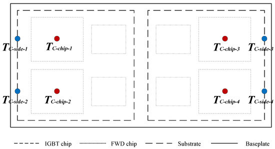
Figure 3.
Placement of thermal sensors for measuring case temperatures.
The measured case temperatures are adopted to estimate the value through (4). The solder aging is decided by observing whether the value changes. When the solder aging occurs, the value is acquired through the updated value. In the second stage, substituting the change of into (7) and (9) to correct the model parameters. Then the junction temperature is predicted by the updated thermal equivalent circuit model. With the above two stages, the thermal equivalent circuit model is corrected timely during the solder aging. The flowchart of the method implementation is in Figure 4.
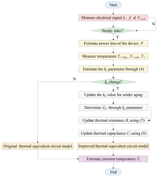
Figure 4.
The flowchart of the method.
3. Simulation Validation
In this section, a finite element analysis (FEA) example is demonstrated to validate the effectiveness of the proposed method. A commercial IGBT module produced by SEMIKRON (Shanghai, China) is modeled through Pro/Engineer software (Version 5.1), as shown in Figure 5. The IGBT model shown in Figure 5 is introduced in ANSYS, a commercial FEA software platform (Version 17.2). Transient thermal analysis of the IGBT model is carried out in ANSYS software (Version 17.2). The operation conditions of the IGBT module are as follows: the DC-link voltage is 300 V, the collector current is 60 A, the switching frequency is 10 kHz, the modulation index is 1, and the line frequency is 50 Hz.
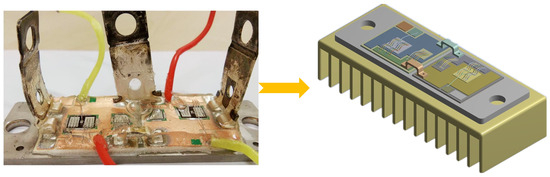
Figure 5.
The three-dimensional IGBT model.
The solder fatigue is simulated by changing the thermal conductivity of the partial region in the solder layer. We set up the following aging scenarios to explore the effect of solder fatigue on the module’s thermal behavior. (1) healthy condition without solder aging; (2) slightly aging, i.e., 10% aging region in the solder layer; (3) minor aging, i.e., 20% aging region in the solder layer; (4) intermediate aging, i.e., 30% aging region in the solder layer; (5) extensive aging, i.e., 40% aging region in the solder layer; (6) dangerous aging, i.e., 50% aging region in the solder layer. In addition, it should be noted that the solder aging gradually expanded from the side to the center.
The power loss of the chip is estimated according to the operation conditions of the IGBT module. The transient thermal analysis is processed by applying the power loss on the IGBT models with various aging conditions. The heat flow results under different aging scenarios are in Figure 6. From Figure 6, the thermal channel of the heat flow spreading down to the baseplate gradually narrowed from scenarios 1 to 6. The heat flow accumulates in the central area of the solder layer, resulting in a continuous increase in heat flux density in the central area with the degradation of the solder. In scenario 6, the heat flow can only be transferred down to the baseplate through the non-cracked area in the solder layer. Therefore, the heat flow is concentrated in the baseplate’s central area, while reduced in the remaining area. Finally, the case temperatures in the central region of the baseplate increase, while the case temperatures in other regions continue to decrease.
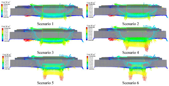
Figure 6.
The heat flow under various solder fatigue states (the arrows in different colors represent various heat fluxes).
The evolution of and during the degradation of solder layer is in Figure 7. gradually increases about 5 °C from scenario 1 to 6. Meanwhile, continues to decrease by about 2.5 °C. and are substituted into (4) to estimate the values under different solder aging conditions. In addition, values are estimated by substituting and into (1). The results of and are in Figure 8.
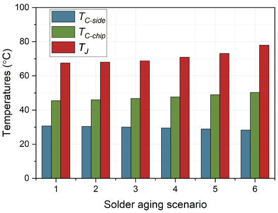
Figure 7.
Evolution of temperatures during solder fatigue.
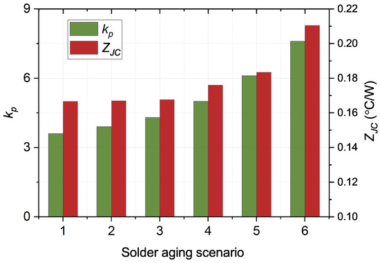
Figure 8.
Evolution of and during solder fatigue.
With the deterioration of solder aging, the values of and increase monotonically, indicating that and are only related to the solder aging. Therefore, a database including and is built based on an offline accelerated aging test. In practice, the solder fatigue is monitored in real time by the parameter. The value is acquired through in the database. Compared with other methods, the parameter only relies on the case temperatures, with an advantage in economy and stability.
Then, the effectiveness of the correction algorithm for the model parameters is verified. The parameters of the thermal equivalent circuit model for a healthy IGBT module are extracted based on the work in [27,28]. The extracted model parameters are in Table 1. Firstly, the performance of the original thermal equivalent circuit model during solder aging is tested. The operation condition and case temperature in scenario 5 are given to the original thermal equivalent circuit model to predict junction temperature. The junction temperature results from the original model and FEA are compared in Figure 9.

Table 1.
Parameters of the original thermal equivalent circuit model.
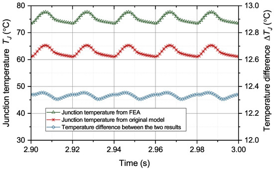
Figure 9.
Temperatures from FEA and the original model.
The difference between the two temperature results is greater than 12 °C most of the time, which greatly exceeds the tolerable error of the temperature prediction. Continued use of this model may cause the module to operate outside the safety threshold. Therefore, it is necessary to correct the model parameters to remove the influence of solder aging. The model parameters are corrected through (7) and (9) based on the information of . The modified model parameters are in Table 2.
Table 2.
Modified parameters of the improved model for the six simulated aging scenarios.
The results in Table 2 show that the value of increases gradually with the deterioration of solder aging, while the value of continues to decrease. Different material properties of the crack and the solder caused this phenomenon. Compared with solder, the thermal conductivity of the crack is lower, and the specific heat capacity is greater. A low thermal conductivity increases , and a high specific heat capacity decreases .
The same operation conditions are applied to the improved thermal equivalent circuit model to predict the junction temperature. The comparison of the junction temperature results from the model and FEA is in Figure 10.
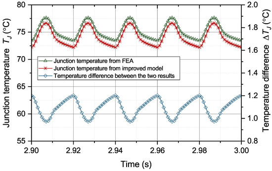
Figure 10.
Temperatures from FEA and the improved model.
From Figure 10, the temperature results from the improved thermal equivalent circuit model can accurately track the temperature results from FEA. The difference between the two temperature results was generally less than 1.2 °C. The correlation between the two signals is more than 0.96. Under the six solder aging scenarios, the mean absolute error (MAE) of junction temperature from the original and improved thermal equivalent circuit models is in Table 3. From Table 3, the temperature prediction error from the original model continues to increase with the deterioration of the solder. Under scenario 6, the prediction error of the original model reaches 32 °C, which is far beyond the tolerance of temperature prediction. Compared with the original model, the improved model can significantly reduce the prediction error by about 90%. As a result, the performance of temperature prediction greatly improved.
Table 3.
Error Statistics of .
4. Experimental Validation
In this section, the effectiveness of the improved thermal equivalent circuit model is validated by an experimental case. The test equipment is in Figure 11, including a commercial IGBT module produced by SEMIKRON (the upper package is removed), an IR camera to measure the chip junction temperature, a recorder for obtaining various electrical signals of the module, a signal generator for offering a driving signal, a DC power supply for the test current, air-cooled equipment to cool the module, and a National Instruments (NI) data acquisition instrument for measuring the case temperatures. Shallow grooves are carved into the upper surface of the heat sink for placing thermal sensors to measure the case temperatures.
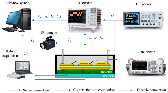
Figure 11.
Experimental setup.
To obtain the evolution of various signals that characterize the IGBT module’s aging conditions, we built an accelerated aging test platform for power devices based on the experimental equipment shown in Figure 11. Applying a 10% overload current to the IGBT module to heat the junction temperature to 180 °C quickly, and then bring down the junction temperature to 60 °C through the air-cooled equipment. In this way, the IGBT module is subject to a 120 °C temperature swing in one thermal cycle.
The starting point of the thermal cycle in Figure 12 is 0, meaning that the IGBT module is a healthy device without thermal damage. Thermal damage occurs to the solder and bond wires when the IGBT module goes through a thermal cycle. The IGBT fails when the thermal damage accumulates to the threshold value. The and are the indicators of solder aging. The values of and rely on temperature information such as , and . The case temperatures containing and are collected in real time by the NI data acquisition instrument during the test, and is measured with the IR camera. The collector–emitter on-voltage indicates the degradation of bond wires, and is collected in real time by the recorder. , and are substituted into (1) and (4) to estimate the values of and , respectively. The results of , and are in Figure 12.
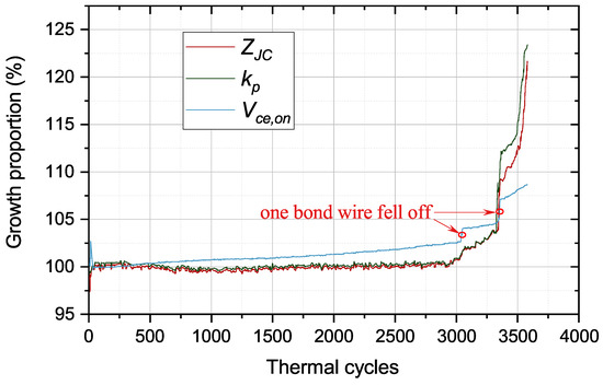
Figure 12.
Evolution of , and during the solder fatigue.
is a core parameter to describe the bond wires’ degradation. The thermal damage to the module containing solder and bond wires has a very slow growth before 3000 thermal cycles. Therefore, the values of , and have a little change. According to the theory of cumulative damage in fatigue, the module’s thermal damage reaches the threshold after 3000 cycles. Accordingly, , and have a rapid growth after 3000 cycles. When one bond wire falls off, increases exponentially, resulting in a big rise in the module’s power loss. As a result, the thermal pressure of the solder layer increases, leading to accelerated solder aging. The growth trend of and is consistent, indicating that and are only related to solder aging. Therefore, the parameter is suited to monitor solder fatigue timely. According to the information of , is acquired during the normal operation of power converter.
A DC pulse current is applied to the IGBT module to examine the performance of the original thermal equivalent circuit model during solder fatigue. The module’s power loss is estimated according to the electrical signal collected by the recorder. The power loss is given to the original thermal equivalent model to predict the junction temperature. The temperature results from the model were compared with that measured by the IR camera, as shown in Figure 13. The IR camera used in this paper is the FOTRIC series, which can continuously collect temperature at a point and obtain a temperature map. Figure 14 shows the temperature distribution of the module’s upper surface. From Figure 14, the temperature at the chip is the highest. The farther away it is from the chip, the cooler it becomes. That is because the chip is the heat source of the IGBT module.
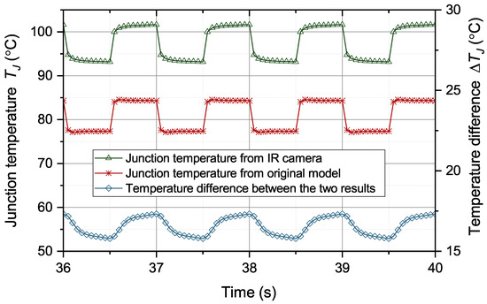
Figure 13.
Temperatures from IR camera and the original model.
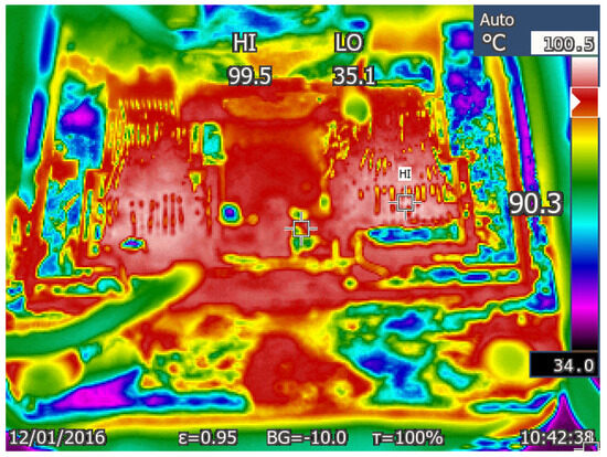
Figure 14.
Temperature results from IR camera.
From Figure 13, the difference between the two temperature results is greater than 15 °C most of the time, with a maximum difference of 17 °C. Continued use of this model may cause the module to operate outside the safety threshold. Therefore, it is necessary to correct the model parameters to remove the effect of solder fatigue. The model parameters are corrected through (7) and (9) based on the information of . The modified model parameters are in Table 4. From Table 4, it can be seen that the experimental results are consistent with the simulation results. The different material properties of the solder and crack lead to the variation in and . The crack has lower thermal conductivity and higher specific heat capacity, resulting in an increase in and a decrease in with the deterioration of the solder.
Table 4.
Modified parameters of the improved model under the specific test aging conditions.
The same operation conditions are applied to the improved thermal equivalent circuit model to predict the junction temperature. The comparison of the junction temperature results from the model and IR camera is in Figure 15. From Figure 15, the temperature results from the improved thermal equivalent circuit model can be seen to accurately track the temperature results from the IR camera. The difference between the two temperature results was generally less than 2 °C. The correlation between the two signals is more than 0.96. The mean absolute error (MAE) of junction temperature from the original and improved thermal equivalent circuit models under the specified solder aging conditions is in Table 5. The simulation and experimental results are consistent. The junction temperature error of the original model increases with the solder aging. The junction temperature error of the original model reaches 16.2 °C when rises by 20%. It is no longer helpful for the thermal management of power devices. Compared with the original model, the junction temperature error from the improved thermal equivalent circuit model is reduced by about 90% under the specified aging conditions. As a result, the performance of temperature prediction greatly improved.
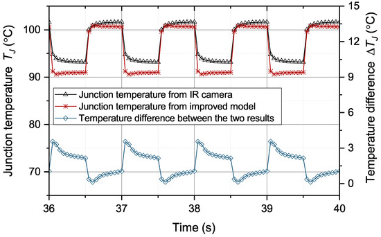
Figure 15.
Temperatures from IR camera and the improved model.
Table 5.
Error Statistics of .
In addition, this work can help students of power electronics courses to understand the thermal failure mechanism of semiconductor power devices and how to improve the reliability of power device operation through temperature monitoring. The semiconductor power device is the core component of energy conversion. In power electronics courses, students only learn the principles of energy conversion through power devices. Most experimental courses are arranged around DC-AC conversion. Students cannot understand the internal structure of the power device, the heat generation mechanism, and the heat dissipation process of the power device. This experimental and simulation analysis can help students have an in-depth knowledge of power devices’ mechanical structure, heat dissipation principles, temperature distribution, junction temperature monitoring, and so on. We suggest that this work can be included in the experimental courses of power electronics to give students a more comprehensive understanding of power devices.
5. Conclusions
This paper proposes an improved thermal equivalent model to predict the junction temperature of the IGBT module. The temperature accuracy from the model still satisfies the precision requirements when the solder aging occurs. Firstly, we propose a parameter to monitor solder aging in real-time. The parameter is only related to the case temperatures, and the parameter continues to increase with the solder aging. The database of and is established according to the accelerated aging test of power devices. During the normal operation of the IGBT module, the value is determined by the parameter. Secondly, we explore the mechanism of solder aging on the thermal equivalent circuit model parameters. An algorithm for modifying model parameters is proposed based on the module’s linear thermal behavior. The changes in are mapped proportionally to the model parameters. Simulation and experimental results validate the effectiveness of the improved model. During the solder aging, the junction temperature prediction errors from the improved model are reduced by about 90% from the original model. The research of this paper plays a significant role in improving the reliability of photovoltaic power generation systems.
Author Contributions
Conceptualization, Z.H. and X.W.; methodology, Z.H.; software, Z.H.; validation, X.W.; formal analysis, M.C.; investigation, Z.H.; resources, Z.H.; data curation, M.C.; writing—original draft preparation, Z.H.; writing—review and editing, Z.H.; visualization, Z.H.; supervision, M.C.; project administration, Z.H.; funding acquisition, Z.H. All authors have read and agreed to the published version of the manuscript.
Funding
This work was funded by a grant from the National Natural Science Foundation (622030527) and Natural Science Research Project of higher education institutions in Jiangsu Province (22KJB470007).
Data Availability Statement
The data presented in this study are available on request from the corresponding author.
Conflicts of Interest
The authors declare no conflicts of interest.
References
- Ji, B.; Song, X.; Cao, W.; Pickert, V.; Hu, Y.; Mackersie, J.W.; Pierce, S.G. In situ diagnostics and prognostics of solder fatigue in IGBT modules for electric vehicle drives. IEEE Trans. Power Electron. 2015, 30, 1535–1543. [Google Scholar] [CrossRef]
- Wolfgang, E. Examples for failures in power electronics systems. Presented at the ECPE Tutorial on Reliability of Power Electronic Systems, Nuremberg, Germany, 19–20 April 2007; pp. 19–20. [Google Scholar]
- Luo, H.; Chen, Y.; Sun, P.; Li, W.; He, X. Junction temperature extraction approach with turn-off delay time for high-voltage high-power IGBT modules. IEEE Trans. Power Electron. 2016, 31, 5122–5132. [Google Scholar] [CrossRef]
- Codecasa, L.; Catalano, A.P.; d’Alessandro, V. A priori error bound for moment matching approximants of thermal models. IEEE Trans. Compon. Packag. Manuf. Technol. 2019, 9, 2383–2392. [Google Scholar] [CrossRef]
- Scognamillo, C.; Catalano, A.P.; Riccio, M.; d’Alessandro, V.; Codecasa, L.; Borghese, A.; Tripathi, R.N.; Castellazzi, A.; Breglio, G.; Irace, A. Compact modeling of a 3.3 kv sic mosfet power module for detailed circuit-level electrothermal simulations including parasitics. Energies 2021, 14, 4683. [Google Scholar] [CrossRef]
- Bahman, A.S.; Ma, K.; Ghimire, P.; Iannuzzo, F.; Blaabjerg, F. A 3-D-lumped thermal network model for long-term load profiles analysis in high-power IGBT modules. IEEE J. Emerg. Sel. Top. Power Electron. 2016, 4, 1050–1063. [Google Scholar] [CrossRef]
- Bahman, A.S.; Ma, K.; Blaabjerg, F. A lumped thermal model including thermal coupling and thermal boundary conditions for high-power IGBT modules. IEEE Trans. Power Electron. 2018, 33, 2518–2530. [Google Scholar] [CrossRef]
- Reichl, J.; Ortizrodriguez, J.M.; Hefner, A.R.; Lai, J. 3-D thermal component model for electrothermal analysis of multichip power modules with experimental validation. IEEE Trans. Power Electron. 2015, 30, 3300–3308. [Google Scholar] [CrossRef]
- Gerstenmaier, Y.C.; Castellazzi, A.; Wachutka, G. Electrothermal simulation of multichip-modules with novel transient thermal model and time-dependent boundary conditions. IEEE Trans. Power Electron. 2006, 21, 45–55. [Google Scholar] [CrossRef]
- Catalano, A.P.; Scognamillo, C.; d’Alessandro, V.; Castellazzi, A. Numerical simulation and analytical modeling of the thermal behavior of single-and double-sided cooled power modules. IEEE Trans. Compon. Packag. Manuf. Technol. 2020, 10, 1446–1453. [Google Scholar] [CrossRef]
- Du, B.; Hudgins, J.L.; Santi, E.; Bryant, A.T.; Palmer, P.R.; Mantooth, H.A. Transient electrothermal simulation of power semiconductor devices. IEEE Trans. Power Electron. 2009, 25, 237–248. [Google Scholar]
- Ouhab, M.; Khatir, Z.; Ibrahim, A.; Ousten, J.-P.; Mitova, R.; Wang, M.-X. New analytical model for real-time junction temperature estimation of multichip power module used in a motor drive. IEEE Trans. Power Electron. 2018, 33, 5292–5301. [Google Scholar] [CrossRef]
- Kostandyan, E.E.; Sørensen, J.D. Reliability of wind turbine components—solder elements fatigue failure. In Proceedings of the 2012 Proceedings Annual Reliability and Maintainability Symposium, Reno, NV, USA, 23–26 January 2012; pp. 1–7. [Google Scholar]
- Evans, P.; Castellazzi, A.; Johnson, C.M. Automated fast extraction of compact thermal models for power electronic modules. IEEE Trans. Power Electron. 2013, 28, 4791–4802. [Google Scholar] [CrossRef]
- Bryant, A.T.; Parkerallotey, N.; Hamilton, D.P.; Swan, I.R.; Mawby, P.A.; Ueta, T.; Nishijima, T.; Hamada, K. A fast loss and temperature simulation method for power converters, part I: Electrothermal modeling and validation. IEEE Trans. Power Electron. 2012, 27, 248–257. [Google Scholar] [CrossRef]
- Swan, I.R.; Bryant, A.T.; Mawby, P.A.; Ueta, T.; Nishijima, T.; Hamada, K. A fast loss and temperature simulation method for power converters, part II: 3-D thermal model of power module. IEEE Trans. Power Electron. 2012, 27, 258–268. [Google Scholar] [CrossRef]
- Gachovska, T.K.; Tian, B.; Hudgins, J.L.; Qiao, W.; Donlon, J.F. A real-time thermal model for monitoring of power semiconductor devices. IEEE Trans. Ind. Appl. 2015, 51, 3361–3367. [Google Scholar] [CrossRef]
- Scognamillo, C.; Fregonese, S.; Zimmer, T.; d’Alessandro, V.; Catalano, A.P. A technique for the in-situ experimental extraction of the thermal impedance of power devices. IEEE Trans. Power Electron. 2022, 37, 11511–11515. [Google Scholar] [CrossRef]
- Nishimura, Y.; Oonishi, K.; Morozumi, A.; Mochizuki, E.; Takahashi, Y. All lead free igbt module with excellent reliability. In Proceedings of the ISPSD’05, The 17th International Symposium on Power Semiconductor Devices and ICs, Santa Barbara, CA, USA, 23–26 May 2005; pp. 79–82. [Google Scholar]
- Sommer, J.-P.; Licht, T.; Berg, H.; Appelhoff, K.; Michel, B. Solder fatigue at high-power igbt modules. In Proceedings of the 4th International Conference on Integrated Power Systems, Naples, Italy, 7–9 June 2006; pp. 1–6. [Google Scholar]
- Arya, A.; Chanekar, A.; Deshmukh, P.; Verma, A.; Anand, S. Accurate online junction temperature estimation of igbt using inflection point based updated i–v characteristics. IEEE Trans. Power Electron. 2021, 36, 9826–9836. [Google Scholar] [CrossRef]
- Hu, Z.; Du, M.; Wei, K.; Hurley, W.G. An adaptive thermal equivalent circuit model for estimating the junction temperature of IGBTs. IEEE J. Emerg. Sel. Top. Power Electron. 2019, 7, 392–403. [Google Scholar] [CrossRef]
- Chen, H.; Ji, B.; Pickert, V.; Cao, W. Real-time temperature estimation for power MOSFETs considering thermal aging effects. IEEE Trans. Device Mater. Reliab. 2014, 14, 220–228. [Google Scholar] [CrossRef]
- Hanif, A.; Roy, S.; Khan, F. Detection of gate oxide and channel degradation in sic power mosfets using reflectometry. In Proceedings of the 2017 IEEE 5th Workshop on Wide Bandgap Power Devices and Applications (WiPDA), Albuquerque, NM, USA, 30 October–1 November 2017; pp. 383–387. [Google Scholar]
- Ji, B.; Pickert, V.; Cao, W.; Zahawi, B. In situ diagnostics and prognostics of wire bonding faults in igbt modules for electric vehicle drives. IEEE Trans. Power Electron. 2013, 28, 5568–5577. [Google Scholar] [CrossRef]
- Wang, X.; Sun, P.; Sun, L.; Luo, Q.; Du, X. Online condition monitoring for bond wire degradation of igbt modules in three-level neutral-point-clamped converters. IEEE Trans. Ind. Electron. 2020, 68, 7474–7484. [Google Scholar] [CrossRef]
- Eleffendi, M.A.; Johnson, C.M. Application of kalman filter to estimate junction temperature in IGBT power modules. IEEE Trans. Power Electron. 2016, 31, 1576–1587. [Google Scholar] [CrossRef]
- Tang, Y.; Ma, H. Dynamic electrothermal model of paralleled IGBT modules with unbalanced stray parameters. IEEE Trans. Power Electron. 2017, 32, 1385–1399. [Google Scholar] [CrossRef]
Disclaimer/Publisher’s Note: The statements, opinions and data contained in all publications are solely those of the individual author(s) and contributor(s) and not of MDPI and/or the editor(s). MDPI and/or the editor(s) disclaim responsibility for any injury to people or property resulting from any ideas, methods, instructions or products referred to in the content. |
© 2023 by the authors. Licensee MDPI, Basel, Switzerland. This article is an open access article distributed under the terms and conditions of the Creative Commons Attribution (CC BY) license (https://creativecommons.org/licenses/by/4.0/).