
Optical Simulation Design of a Short Lens Length with a Curved Image Plane and Relative Illumination Analysis


 ,
,
Abstract
:1. Introduction
2. Methodology
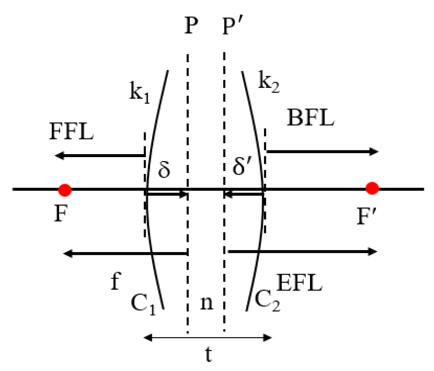
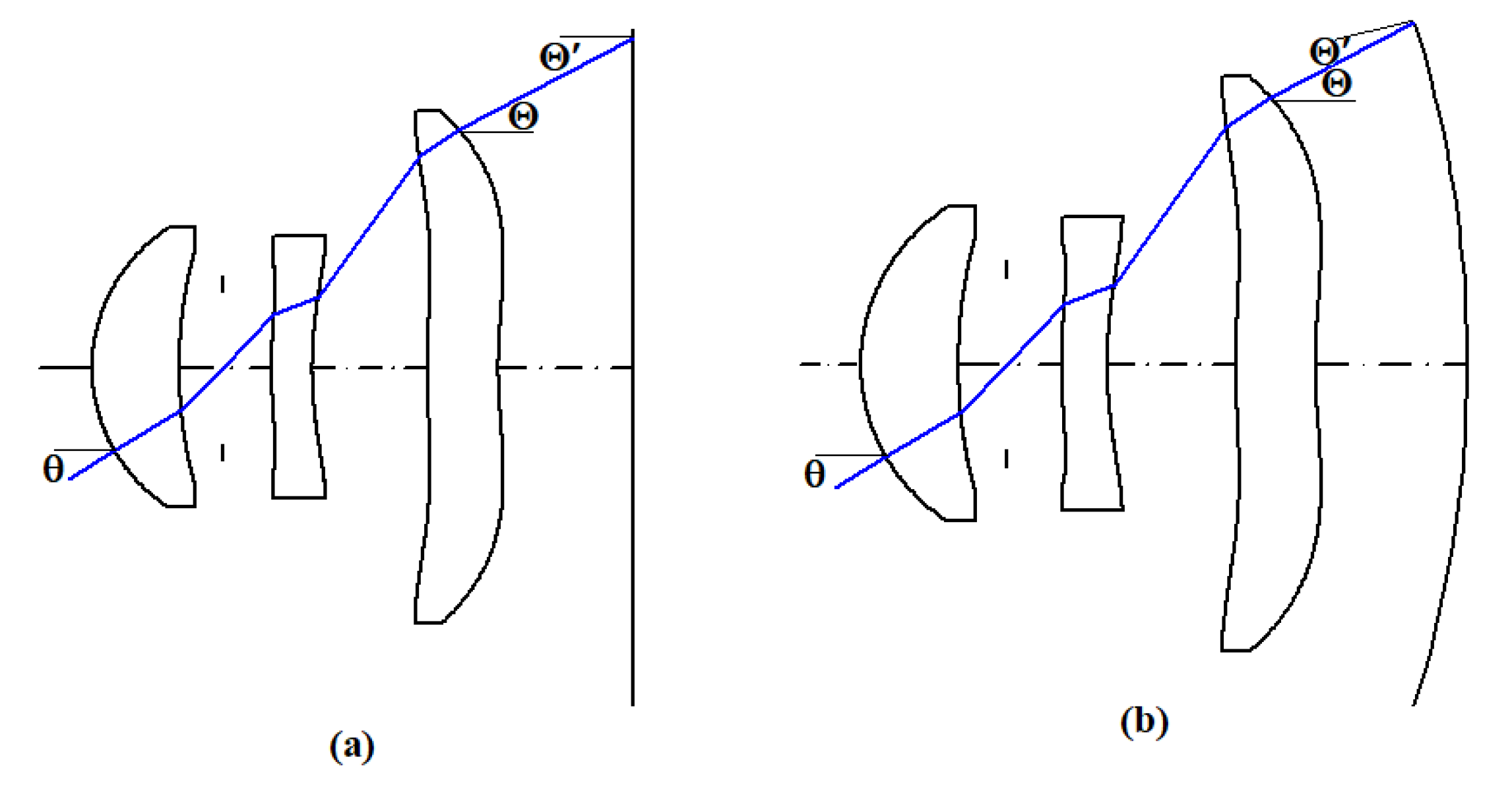
2.1. Lens Length Definition
2.2. First-Order Lens Design
2.2.1. First-Order Design of a Single Lens
2.2.2. First-Order Design of the Three Lenses
2.3. Relative Illumination
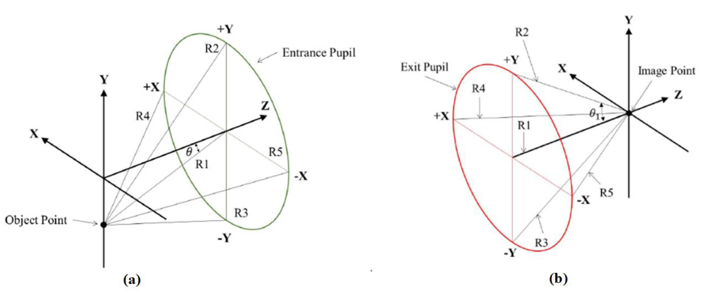
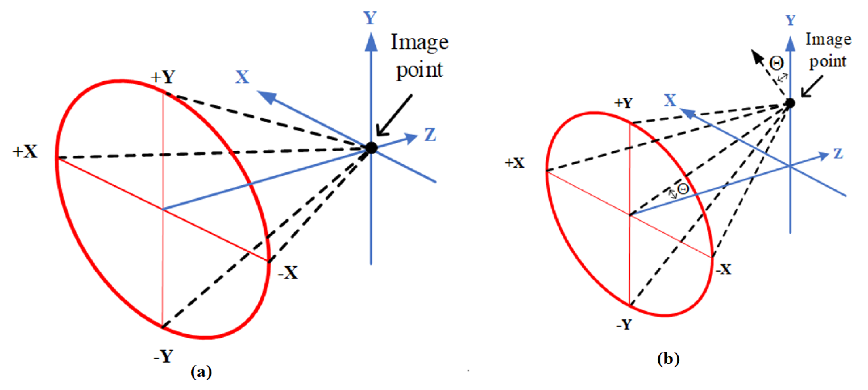
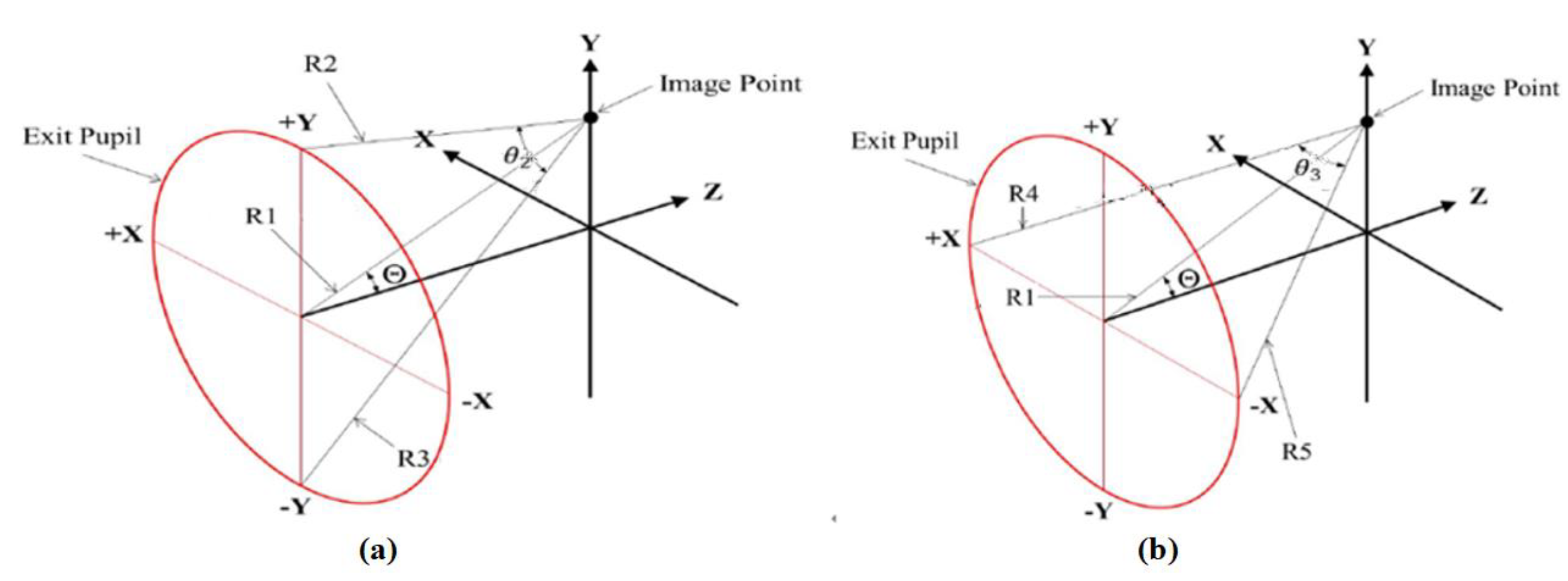
2.3.1. Definition of Solid Angle
2.3.2. Surface Transmittance
2.3.3. Internal Transmittance
2.3.4. Relative Illumination Equation
3. Design Results
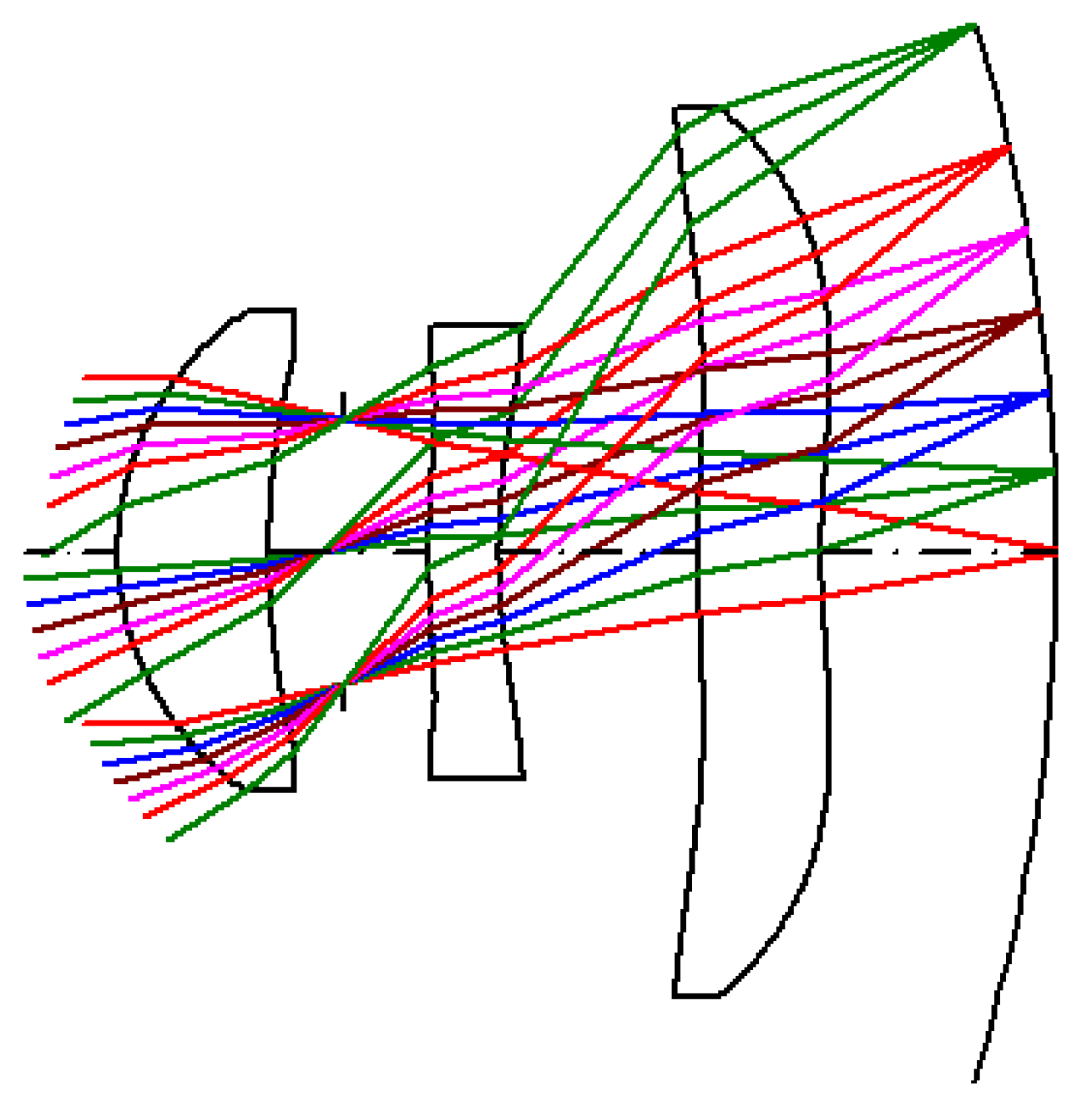
3.1. Lens Length
3.2. Relation Illumination
3.2.1. Projected Solid Angle
3.2.2. Surface Transmittance
3.2.3. Internal Transmittance
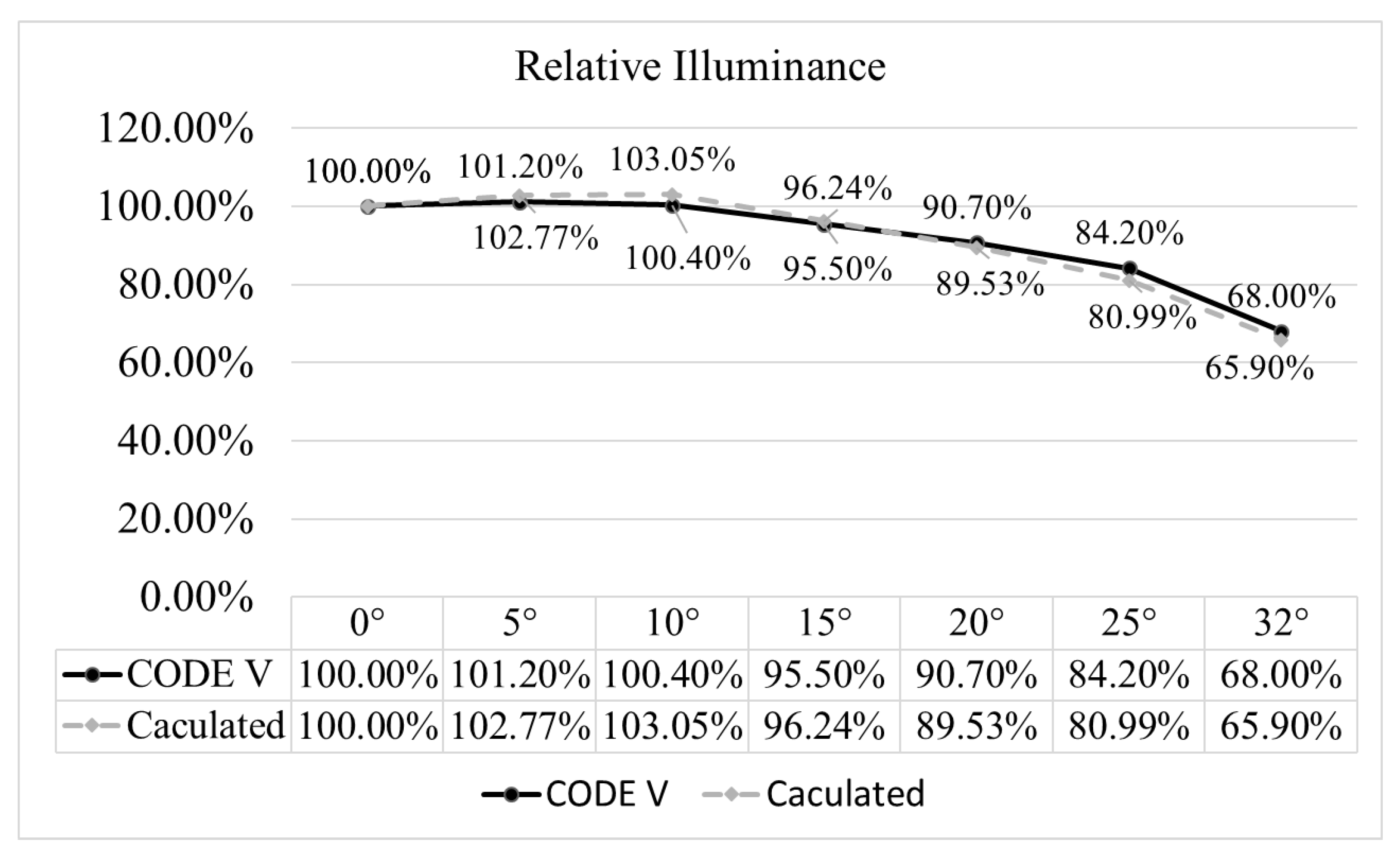
3.2.4. Calculations and Comparisons of the Relative Illuminance
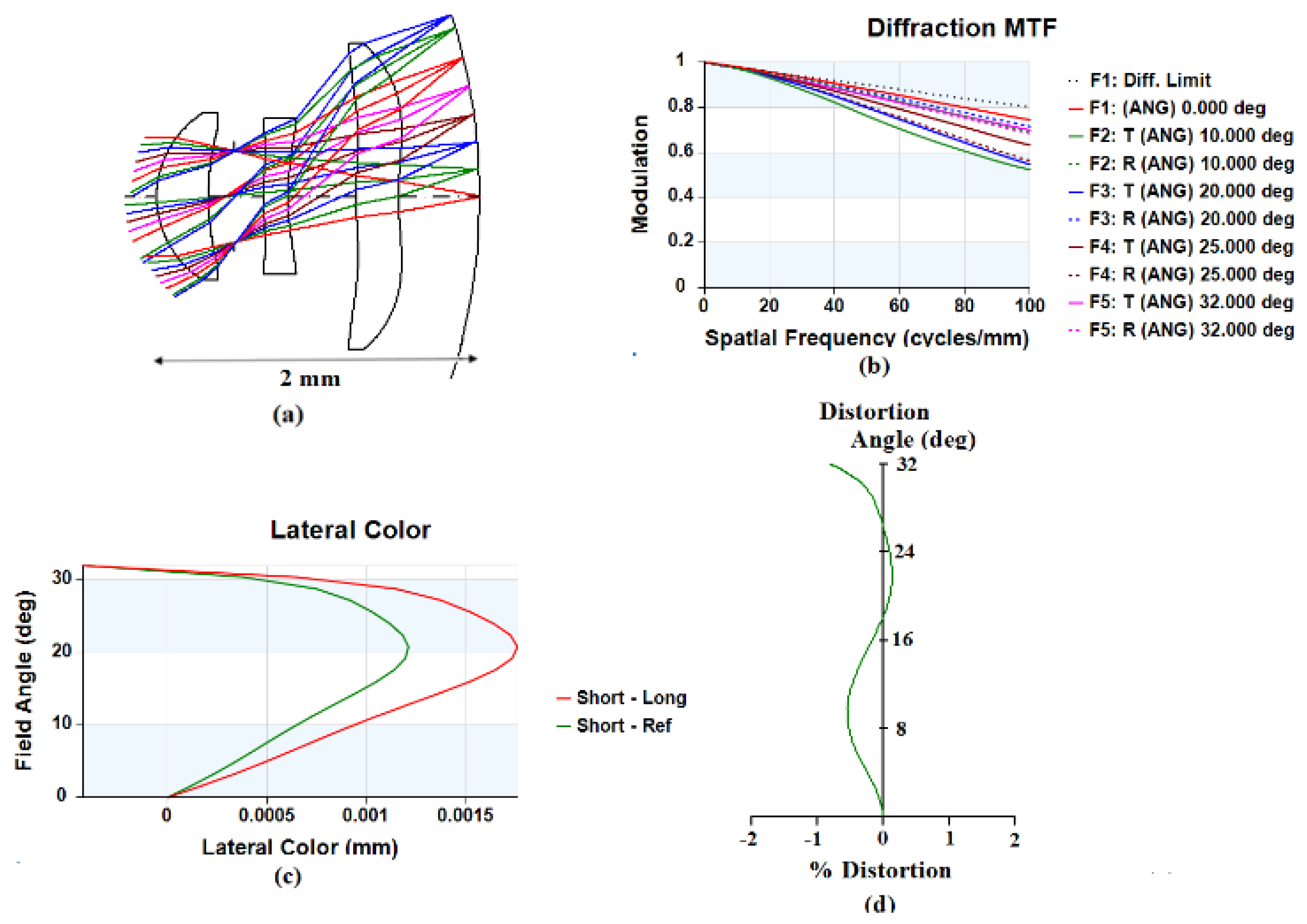
3.3. Image-Quality Analysis of the Three-Lens Design with a Curved Image Plane
4. Conclusions
Author Contributions
Funding
Data Availability Statement
Acknowledgments
Conflicts of Interest
References
- Gaoa, W.; Xub, Z.; Hanb, X.; Pan, C. Recent advances in curved image sensor arrays for bioinspired vision system. Nano Today 2022, 42, 101366. [Google Scholar] [CrossRef]
- Gaschet, C.; Jahn, W.; Chambion, B.; Hugot, E.; Behaghel, T.; Lombardo, S.; Lemared, S.; Ferrari, M.; Caplet, S.; Gétin, S.; et al. Methodology to design optical systems with curved sensors. Appl. Opt. 2019, 58, 973–978. [Google Scholar] [CrossRef] [PubMed]
- Swain, P.; Channin, D.J.; Taylor, G.C.; Lipp, S.A.; Mark, D.S. Curved CCDs and their application with astronomical telescopes and stereo panoramic cameras. In Proceedings of the Sensors and Camera Systems for Scientific, Industrial, and Digital Photography Applications V, San Jose, CA, USA, 19–21 January 2004. [Google Scholar]
- Rim, S.B.; Catrysse, P.B.; Dinyari, R.; Huang, K.; Peumans, P. The optical advantages of curved focal plane arrays. Opt. Express 2008, 16, 4965–4971. [Google Scholar] [CrossRef] [PubMed]
- Iwert, O.; Delabre, B. The challenge of highly curved monolithic imaging detectors. In Proceedings of the High Energy, Optical, and Infrared Detectors for Astronomy IV, San Diego, CA, USA, 27–30 June 2010. [Google Scholar]
- Dumas, D.; Fendler, M.; Baier, N.; Primot, J.; Le Coarer, E. Curved focal plane detector array for wide field cameras. Appl. Opt. 2012, 51, 5419–5424. [Google Scholar] [CrossRef] [PubMed]
- Itonaga, K.; Arimura, T.; Matsumoto, K.; Kondo, G.; Terahata, K.; Makimoto, S.; Baba, M.; Honda, Y.; Bori, S.; Kai, T.; et al. A novel curved CMOS image sensor integrated with imaging system. In Proceedings of the 2014 Symposium on VLSI Technology (VLSI-Technology): Digest of Technical Papers, Honolulu, HI, USA, 9–12 June 2014. [Google Scholar]
- Reshidko, D.; Sasian, J. Optical analysis of miniature lenses with curved imaging surfaces. Appl. Opt. 2015, 54, E216–E223. [Google Scholar] [CrossRef]
- Chen, X.; Gere, D.S.; Waldon, M.C. Small form Factor High-Resolution Camera. U.S. Patent No. 9244253 B2, 26 January 2016. [Google Scholar]
- Guenter, B.K.; Emerton, N. Lenses for Curved Sensor Systems. U.S. Patent No 9,465,191, 11 October 2016. [Google Scholar]
- Gaschet, C.; Chambion, B.; Getin, S.; Moulin, G.; Vandeneynde, A.; Caplet, S.; Henry, D.; Hugot, E.; Jahn, W.; Behaghel, T.; et al. Curved sensors for compact high-resolution wide field designs. In Proceedings of the SPIE Optical Engineering + Applications, San Diego, CA, USA, 6–10 August 2017. [Google Scholar]
- Zuber, F.; Chambion, B.; Gaschet, C.; Caplet, S.; Nicolas, S.; Charrière, S.; Henry, D. Tolerancing and characterization of curved image sensor systems. Appl. Opt. 2020, 59, 8814–8821. [Google Scholar] [CrossRef]
- Sun, W.S.; Tien, C.L.; Pan, J.W.; Huang, K.C.; Chu, P.Y. Simulation of autofocus lens design for a cell phone camera with object distance from infinity to 9.754 mm. Appl. Opt. 2015, 54, E203–E209. [Google Scholar] [CrossRef] [PubMed]
- Synopsys Inc. Code V Electronic Document Library, Version 10.5; Lens System Setup for Reference Manuals; CvberArk Software Ltd.: Massachusetts, NE, USA, 2012; Chapter 1. [Google Scholar]
- Fowles, G.R. Introduction to Modern Optics, 2nd ed.; Holt Rinehart and Winston Inc.: Austin, TX, USA, 1975. [Google Scholar]
- Schott. Schott: TIE-35 Transmittance of Optical Glass. In Schott Technical information; Schott Inc.: Mainz, Germany, 2005. [Google Scholar]


| Surface No. | Surface Type | Radius (mm) | Thickness (mm) | Glass | Full Aperture |
|---|---|---|---|---|---|
| Object | Infinity | Infinity | |||
| 1 | Asphere | 0.60809 | 0.32193 | 48,656.84468 (N-FK51A) | 1.03479 |
| 2 | Asphere | 1.71796 | 0.15826 | 0.86572 | |
| Stop | Infinity | 0.18291 | 0.56611 | ||
| 4 | Asphere | 2.05032 | 0.15000 | 75,620.27580 (SF4) | 0.78493 |
| 5 | Asphere | 1.48313 | 0.42407 | 0.96893 | |
| 6 | Asphere | 2.22951 | 0.26284 | 68,893.31250 (P-SF8) | 1.78978 |
| 7 | Asphere | 1.50771 | 0.50000 | 1.89707 | |
| Image | −3.72562 | 0.00000 | 2.25493 |
| Surface No. | K | A | B | C | D |
|---|---|---|---|---|---|
| 1 | −5.0530 × 10⁻¹ | 1.5254 × 10⁻¹ | 1.44297 | −4.21545 | 1.3683 × 101 |
| 2 | 3.18955 | 1.7895× 10⁻³ | 1.2202 × 10⁻¹ | −9.9545 × 10⁻¹ | −5.2982 × 10⁻¹ |
| 4 | 2.70553 | −6.4165 × 10⁻¹ | −5.88438 | 3.1152 × 101 | −1.8758 × 10² |
| 5 | 5.65199 | −4.7730 × 10⁻¹ | −1.51130 | −2.27032 | 2.8802 × 10⁻¹ |
| 6 | −1.000 × 10² | −5.7731 × 10⁻¹ | 7.0377 × 10⁻¹ | −2.1970 × 10⁻¹ | −4.5454 × 10⁻² |
| 7 | −8.5819 × 101 | −3.9086 × 10⁻¹ | −5.8701 × 10⁻² | 1.4844 × 10⁻¹ | −7.1665 × 10⁻² |
| δ′ = −1.48405 mm | |||
|---|---|---|---|
| k | 0.50403 (1/mm) | k12 | 0.51154 (1/mm) |
| d1 | 0.99592 mm | n3 | 1.68893 |
| d2 | 0.73646 mm | t3 | 0.26284 mm |
| k1 | 0.56600 (1/mm) | k31 | 0.30901 (1/mm) |
| k2 | −0.12483 (1/mm) | k3 | −0.12596 (1/mm) |
| θ | Θ | NAX | NAY | Ω | Ω′ |
|---|---|---|---|---|---|
| 0 | 0 | 0.18469 | 0.18467 | 0.10714 sr | 0.10714 sr |
| 5° | 5.24354° | 0.18630 | 0.18894 | 0.11058 sr | 0.11012 sr |
| 10° | 9.79328° | 0.18702 | 0.19080 | 0.11210 sr | 0.11047 sr |
| 15° | 13.71356° | 0.18461 | 0.18330 | 0.10630 sr | 0.10327 sr |
| 20° | 16.20176° | 0.18099 | 0.17599 | 0.10007 sr | 0.09609 sr |
| 25° | 15.66270° | 0.17740 | 0.16322 | 0.09097 sr | 0.08759 sr |
| 32° | 8.54314° | 0.17266 | 0.14080 | 0.07637 sr | 0.07552 sr |
| Half Field Angle θ | Projected Solid Angle | |||
|---|---|---|---|---|
| 656.27 nm | 587.56 nm | 486.13 nm | Average | |
| 0° | 0.10638 | 0.10717 | 0.10862 | 0.10739 |
| 5° | 0.10931 | 0.11012 | 0.11163 | 0.11035 |
| 10° | 0.10973 | 0.11047 | 0.11184 | 0.11068 |
| 15° | 0.10268 | 0.10327 | 0.10435 | 0.10344 |
| 20° | 0.09563 | 0.09609 | 0.09695 | 0.09622 |
| 25° | 0.08730 | 0.08759 | 0.08815 | 0.08768 |
| 32° | 0.07534 | 0.07552 | 0.07596 | 0.07561 |
| Surface No. | Glass Material | s-Polarized Reflectance | p-Polarized Reflectance | un-Polarized Reflectance | Surface Transmittance |
|---|---|---|---|---|---|
| 1 | N-FK51A | 0.01518 | 0.01518 | 0.01518 | 0.98482 |
| 2 | air | 0.01518 | 0.01518 | 0.01518 | 0.98482 |
| 4 | SF4 | 0.00166 | 0.00166 | 0.00166 | 0.99834 |
| 5 | air | 0.00166 | 0.00166 | 0.00166 | 0.99834 |
| 6 | P-SF8 | 0.00360 | 0.00360 | 0.00360 | 0.99640 |
| 7 | air | 0.00360 | 0.00360 | 0.00360 | 0.99640 |
| Total | 0.95970 | ||||
| Half Field Angle | Surface Transmittance | |||
|---|---|---|---|---|
| 656.27 nm | 587.56 nm | 486.13nm | Average | |
| 0° | 0.95010 | 0.95970 | 0.92751 | 0.94569 |
| 5° | 0.94998 | 0.95969 | 0.92775 | 0.94573 |
| 10° | 0.94964 | 0.95950 | 0.92789 | 0.94560 |
| 15° | 0.94882 | 0.95882 | 0.92731 | 0.94491 |
| 20° | 0.94667 | 0.95710 | 0.93105 | 0.94490 |
| 25° | 0.93938 | 0.95161 | 0.92347 | 0.93810 |
| 32° | 0.88188 | 0.89806 | 0.87549 | 0.88514 |
| Glass Materials | Internal Transmittance | ||
|---|---|---|---|
| Wavelength | 656.27 nm | 587.56 nm | 486.13 nm |
| N-FK51A | 0.9980 | 0.9980 | 0.9980 |
| N-SF4 | 0.9980 | 0.9980 | 0.9965 |
| P-SF8 | 0.9940 | 0.9940 | 0.9892 |
| Lens No. | Glass Materials | Thickness (mm) | Internal Transmittance |
|---|---|---|---|
| 1 | N-FK51A | 0.32193 | 0.99994 |
| 2 | N-SF4 | 0.15000 | 0.99997 |
| 3 | P-SF8 | 0.26284 | 0.99984 |
| Total | 0.99975 | ||
| Semi Field Angle | Internal Transmittance | |||
|---|---|---|---|---|
| 656.27 nm | 587.56 nm | 486.13 nm | Average | |
| 0° | 0.99975 | 0.99975 | 0.99960 | 0.99970 |
| 5° | 0.99981 | 0.99989 | 0.99940 | 0.99970 |
| 10° | 0.99981 | 0.99989 | 0.99938 | 0.99969 |
| 15° | 0.99981 | 0.99988 | 0.99937 | 0.99969 |
| 20° | 0.99981 | 0.99982 | 0.99936 | 0.99966 |
| 25° | 0.99981 | 0.99988 | 0.99938 | 0.99969 |
| 32° | 0.99981 | 0.99984 | 0.99963 | 0.99976 |
| Semi Field Angle | Relative Illuminance | |||
|---|---|---|---|---|
| 656.27 nm | 587.56 nm | 486.13 nm | Average | |
| 0° | 100.00% | 100.00% | 100.00% | 100.00% |
| 5° | 102.75% | 102.77% | 102.78% | 102.77% |
| 10° | 103.10% | 103.07% | 102.99% | 103.05% |
| 15° | 96.40% | 96.29% | 96.03% | 96.24% |
| 20° | 89.57% | 89.43% | 89.57% | 89.53% |
| 25° | 81.14% | 81.05% | 80.78% | 80.99% |
| 32° | 65.74% | 65.95% | 66.01% | 65.90% |
Disclaimer/Publisher’s Note: The statements, opinions and data contained in all publications are solely those of the individual author(s) and contributor(s) and not of MDPI and/or the editor(s). MDPI and/or the editor(s) disclaim responsibility for any injury to people or property resulting from any ideas, methods, instructions or products referred to in the content. |
© 2023 by the authors. Licensee MDPI, Basel, Switzerland. This article is an open access article distributed under the terms and conditions of the Creative Commons Attribution (CC BY) license (https://creativecommons.org/licenses/by/4.0/).
Share and Cite
Sun, W.-S.; Tien, C.-L.; Liu, Y.-H.; Huang, G.-E.; Hsu, Y.-S.; Su, Y.-L. Optical Simulation Design of a Short Lens Length with a Curved Image Plane and Relative Illumination Analysis. Micromachines 2024, 15, 64. https://doi.org/10.3390/mi15010064
Sun W-S, Tien C-L, Liu Y-H, Huang G-E, Hsu Y-S, Su Y-L. Optical Simulation Design of a Short Lens Length with a Curved Image Plane and Relative Illumination Analysis. Micromachines. 2024; 15(1):64. https://doi.org/10.3390/mi15010064
Chicago/Turabian StyleSun, Wen-Shing, Chuen-Lin Tien, Yi-Hong Liu, Guan-Er Huang, Ying-Shun Hsu, and Yi-Lun Su. 2024. "Optical Simulation Design of a Short Lens Length with a Curved Image Plane and Relative Illumination Analysis" Micromachines 15, no. 1: 64. https://doi.org/10.3390/mi15010064
APA StyleSun, W.-S., Tien, C.-L., Liu, Y.-H., Huang, G.-E., Hsu, Y.-S., & Su, Y.-L. (2024). Optical Simulation Design of a Short Lens Length with a Curved Image Plane and Relative Illumination Analysis. Micromachines, 15(1), 64. https://doi.org/10.3390/mi15010064