Abstract
We have developed a novel phase modulator, based on fin-type electrodes placed at self-imaging positions of a silicon multimode interference (MMI) waveguide, which allows reduced scattering losses and relaxes the fabrication tolerance. The measured propagation losses and spectral bandwidth are 0.7 dB and 33 nm, respectively, on a 987 μm-long phase shifter. Owing to the self-imaging effect in the MMI waveguide, the wave-front expansion to the electrode was counteracted, and therefore, the scattering loss caused by electrode fins was successfully mitigated. As a proof-of-concept for the MMI-based phase modulator applications, we performed optical modulation based on Mach–Zehnder interferometers (MZIs). The π shift current of the modulator was 1.5 mA.
1. Introduction
Silicon (Si) photonics densely integrate optical devices, incorporating P–N junctions that enable the development of advanced devices, such as high-speed modulators, matrix switches, and variable attenuators [1,2,3,4,5,6,7].
One of the most common problems in Si photonics is the combination of channel waveguides and rib waveguides. Rib structures need large bending radii, which can cause large footprints. Combining a channel waveguide and rib waveguide is ideal for realizing more compact Si photonic circuits. However, a major issue in silicon photonics is the cost. Additional masks and processes are required to fabricate a rib structure [8].
Therefore, in this paper, we propose a novel optical phase modulator with a fin-type electrode based on a multimode interferometer (MMI) waveguide. It is noteworthy that our phase modulator has a wide working wavelength range. Furthermore, it can be fabricated at a low cost, because the minimum line width for processing the modulator is 0.4 μm.
2. Principle and Design
2.1. Princple
We used the carrier-injection method for fabricating a phase modulator composed of an MMI, as shown in Figure 1. The phase modulator is comprised of a multimode waveguide and is connected to a single-mode waveguide. The MMI causes periodic self-imaging of an input field profile [9].
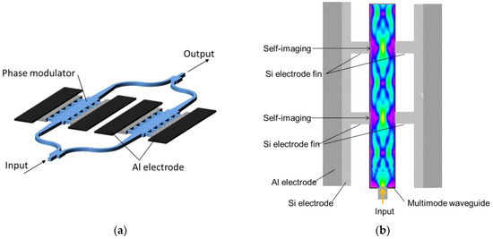
Figure 1.
Schematic of (a) a Mach–Zehnder interferometer modulator with a multimode interferometer (MMI) phase modulator, and (b) a phase modulator based on MMI.
As shown in Figure 1b, the electrode fins are placed at a distance where the self-imaging of an input field occurs. As a result, the scattering loss in the phase modulator caused by the electrode fins is reduced.
2.2. Design of the Phase Modulator
First, we determine the MMI length of the phase modulator via finite-difference time domain calculations under transverse electric-like polarization. The width of the MMI waveguide is ~1.2 μm, and the Si layer thickness is 0.2 μm, which provides a period length of 2.35 μm for self-imaging. A taper was inserted between the single-mode and multimode waveguides for reducing the connection loss. The length of the taper was 9 μm, and the width increased from 0.4 μm to 0.85 μm.
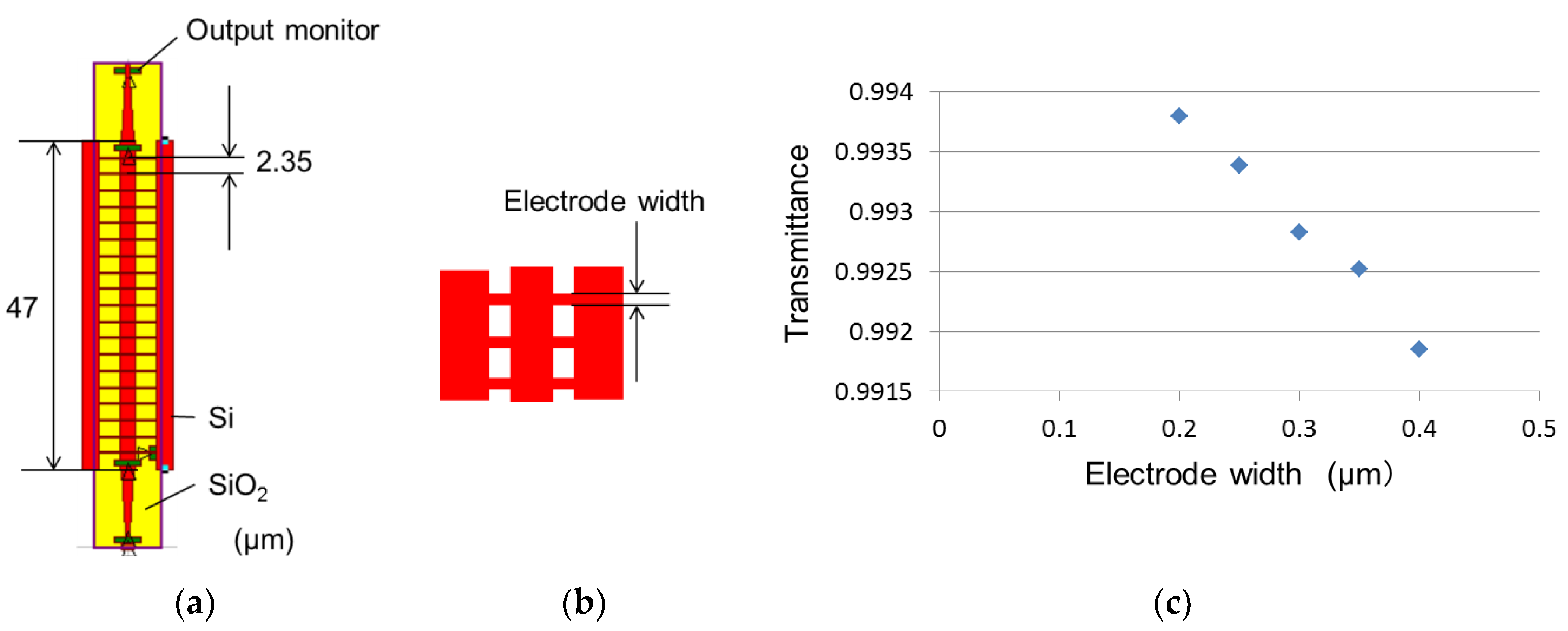
Next, we simulated propagation loss in the waveguide with electrode fins. Figure 2a shows the calculation model of the MMI phase modulator; the electrode width is defined in Figure 2b. Figure 2c shows the propagation loss in the multimode waveguide as a function of the electrode width. Figure 2c indicates that increasing the electrode width increases the propagation loss. However, the propagation loss in the waveguide with an electrode width of 0.4 μm is sufficiently thin for practical application. In addition to the propagation loss, the fabrication process was optimized for a line width of 0.4 μm. We fixed the width of the electrode fin to 0.4 μm for the above reasons.
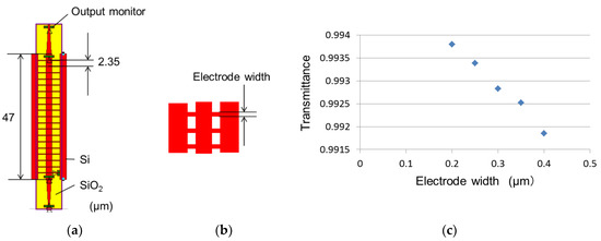
Figure 2.
(a) Numerical calculation model of MMI phase modulator, (b) magnified drawing of electrode fin, and (c) transmittance (based on calculation results).
2.3. Device Structure of the Optical Modulator
Our optical modulator is based on Mach–Zehnder interferometers (MZIs). We fabricated our MZI-based modulator using the MMI phase modulator with fin-type electrodes, as shown in Figure 1a. We fabricated two types of MZI modulators. One modulator had a different optical path, referred so as an asymmetric MZI. The other has the same optical path, called a symmetric MZI.
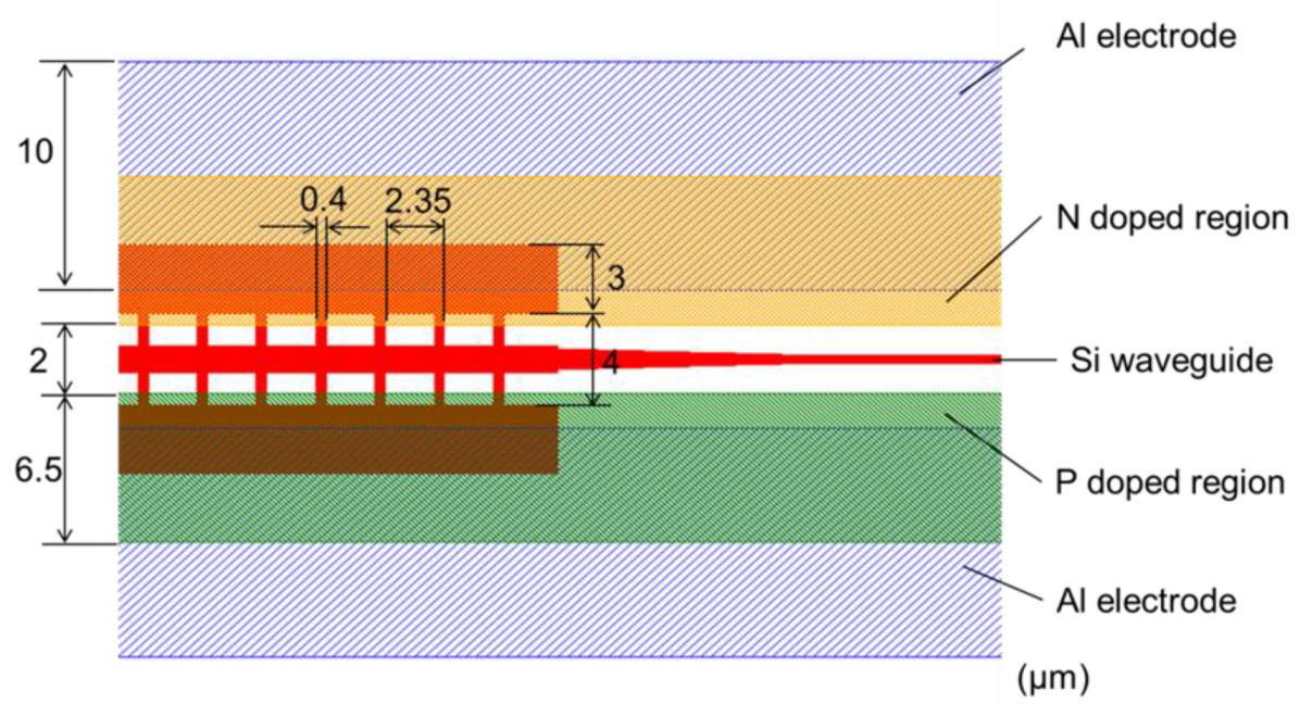
Figure 3 shows the layout of the phase modulator based on an MMI. The length of the electrode fin is 1.4 μm. The P–N region at the side of the MMI phase modulator comprises highly doped P (4 × 1015 cm−2) and N (1 × 1015 cm−2) regions. This modulator only needs P and N regions. The gap between the P-type and N-type areas is 2 μm. A 0.5-μm-thick aluminum (Al) electrode is deposited on silicon (Si). The Si waveguide and Al electrode are covered with a 3-μm-thick oxide silicon layer and a 4-μm-thick SiO2 layer as the upper cladding layer. A 0.3-μm-thick tantalum layer was deposited on SiO2 as the heater.
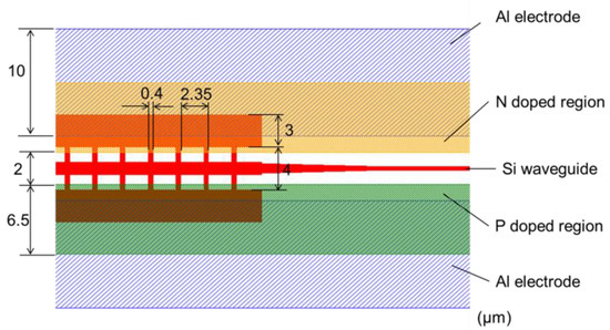
Figure 3.
Layout of a phase modulator based on MMI.
Figure 4a shows the scanning electron microscope (SEM) images of the MMI phase modulator with fins before the deposition of the oxide silicon layer. Figure 4b shows the optical microscope image of the MZI-based modulator formed using this MMI phase modulator with electrode fins.
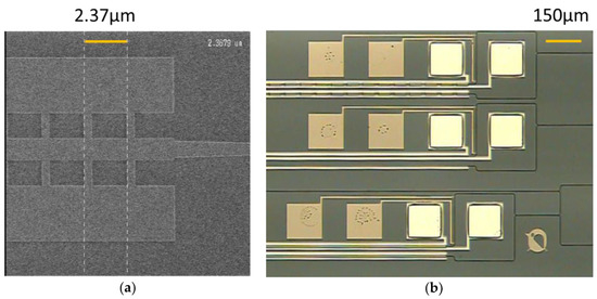
Figure 4.
(a) Scanning electron microscope (SEM) image of an MMI waveguide with fins, and (b) an optical microscope image of a Mach–Zehnder interferometer (MZI) modulator formed using an MMI phase modulator. Orange lines indicate the scale.
3. Experimental Results
3.1. Propagation Loss and Transmission Spectrum of a Multimode Interference Phase Shifter
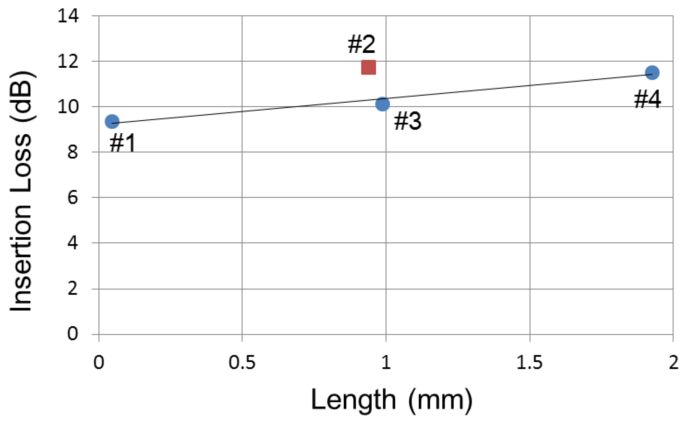
We outsourced the fabrication of the photonics-integrated circuit. The foundry used electron beam lithography for the fabrication. The pitch here is about 0.4 μm, and we can achieve this with deep ultraviolet (UV) lithography, which has low cost for mass production. We fabricated four types of MMI waveguides with fins for measuring the propagation loss, as shown in Figure 5; in this figure, #1 represents 47 μm of the MMI waveguide length with fins, which is the same shape as was obtained via numerical calculation. Furthermore, #2 represents the 20 stages of cascade connections for 47 μm of the MMI waveguide length with fins. It is difficult to estimate small propagation losses in these samples. Therefore, we prepared #2 as a cascade connection of #1. In addition, #3 represents 987 μm of the MMI waveguide length with fins. Finally, #4 represents 1927 μm of the MMI waveguide length with fins.
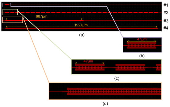
Figure 5.
(a) Four types of MMI waveguides with fins for measuring propagation loss, and magnified drawing of (b) waveguide #1, (c) waveguide #2, and (d) waveguide #3.
The light of the laser source is injected in the input facet of the device by butt coupling through a focused single mode fiber, and it is collected with a multimode fiber. The wavelength of the laser light was 1550 nm. For comparison, we measured the insertion loss in a single-mode waveguide with different lengths on the same wafer. To extract the propagation losses of the MMI waveguide, we drew a linear regression of the output power versus the length of devices 1, 3, and 4, as shown in Figure 6. We evaluated the insertion loss of an MMI waveguide with fins as 1.1 dB/mm from the coefficient of the result of the linear regression. The offset value of the linear regression of 9.2 dB, including the connection loss of a pair of tapers and the coupling loss at both the input and output ends between the spot size converter (SSC) and fiber. Assuming that the insertion losses and the propagation losses of the MMI waveguide are the same, we can predict the insertion loss of an MMI waveguide with 0.94 μm of length as 10.28 dB. However, the insertion loss of #2 was 11.74 dB, as shown in Figure 6. We consider that the difference is caused by the cascade connection of tapers. The differential number of tapers between waveguide #2 and #3 is 19 pairs. We estimated that the connection loss of a pair of tapers is 0.08 dB. The propagation loss in the straight waveguide on the same wafer was 0.32 dB/mm; there are 422 fins per 1 mm of MMI waveguide. We evaluated the scattering loss of a fin as 0.0018 dB. We considered that the insertion loss of the MMI waveguide with fins is considered sufficient for practical use.
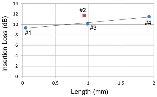
Figure 6.
Length dependence of the insertion loss of an MMI waveguide with fins.
We measured the transmission spectrum for 987 μm of the MMI waveguide length with fins. We input light waves emitted from a super-luminescent laser diode (SLD) into the MMI waveguide with fins with a tapered fiber, and measured the transmission spectrum using an optical spectrum analyzer (OSA). As a reference, we measured the spectrum of the SLD. Figure 7 shows the transmission spectrum of the MMI waveguide with fins. The full width at half maximum (FWHM) in the transmission spectrum of the MMI waveguide with fins was 33 nm. We decided that 987 μm of length would be appropriate for phase modulators, owing to the aforementioned reason.
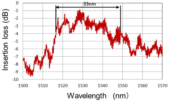
Figure 7.
Transmission spectrum of an MMI waveguide with fins.
3.2. Shift in Transmission Spectrum and Modulation by Current Injection
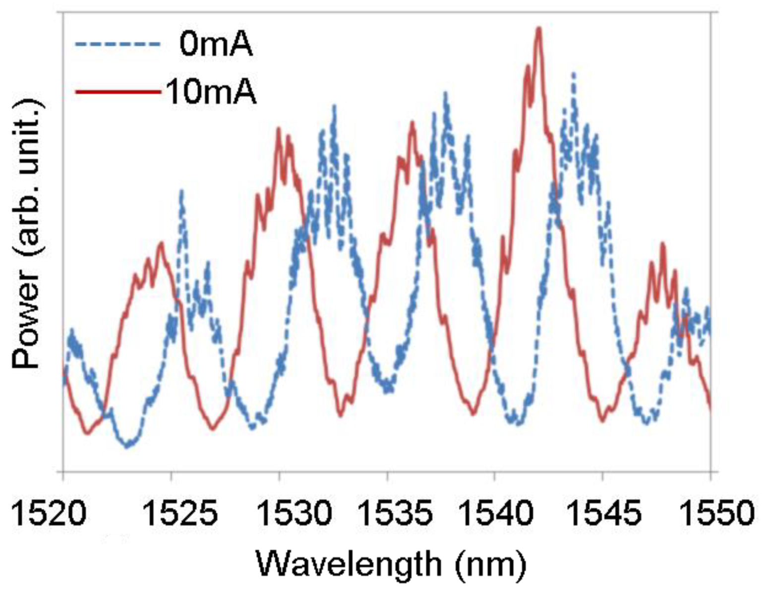
First, we measured the shift in the transmission spectrum of the asymmetric MZI modulator. We contacted the P and N electrodes with needle probes and injected the forward bias current. We input light waves delivered from the SLD into the MZI modulator with a tapered fiber, and measured the transmission spectrum with the OSA. Figure 8 shows the output spectrum of the MZI modulator under injection currents of 0 mA and 10 mA. On increasing the injection current, the peaks shifted toward shorter wavelengths. When the carrier plasma effect occurs, increasing the carrier density decreases the refractive index. On the other hand, increasing the temperature will increase the refractive index. We confirmed that this wavelength shift was caused by the carrier plasma effect.

Figure 8.
Shift in transmission spectrum of an MZI-based modulator with an MMI phase modulator caused by current injection.
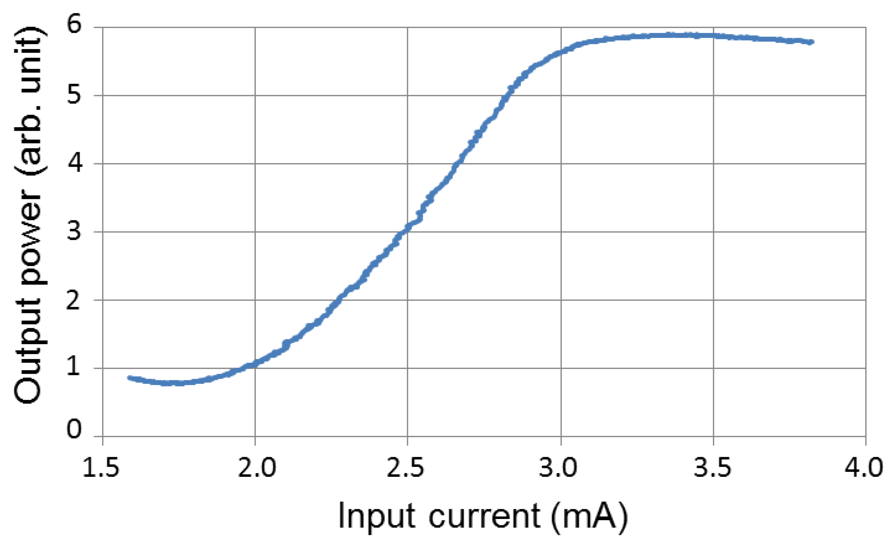
Next, we attempted to modulate light waves. We input laser light into the symmetric MZI modulator with a tapered fiber and coupled the output light with a multimode fiber. The wavelength of the light was 1550 nm. We applied alternating current (AC) at 10 MHz to the MZI modulator. The optical output was detected using an optical/electrical converter (1444-50, Newport, Irvine, CA, USA). Electrical signals were captured by using a sampling oscilloscope (MSO4104, Agilent, Santa Clara, CA, USA). Figure 9 and Figure 10 show the measurement results of the modulated light waves. We measured output power, as a function of the injection current. It appears that the injection current reached the half-wave current, because both the ceiling and floor of the waveforms were distorted.
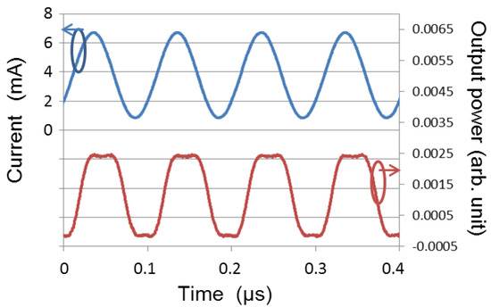
Figure 9.
Output power of an MZI modulator with MMI phase modulator driven by alternating current (AC) power.

Figure 10.
Injection current dependence of output power of an MZI modulator with an MMI phase modulator.
4. Discussion
Here, we discuss the issues pertaining to MMI phase shifters. When light passes through an MMI structure, internal reflection occurs. In our experiment, we observed some ripples, which are indicated in the transmission spectrum shown in Figure 8.
The free spectrum range (FSR) of a Fabry–Perot resonator is expressed as
where λ is the wavelength, and nr and l represent the refractive index and length of the cavity, respectively. The period of the ripples in the transmission spectrum of the MMI waveguide shown in Figure 8 is 0.55 nm; the measurement wavelength is 1.55 μm. The length of the phase shifter is 987 μm. The refractive index of the silicon waveguide was calculated to be 2.1. Since not one mode but a few modes propagate through an MMI waveguide, we calculated the FSR of the MMI waveguide with an average refractive index; the FSR was predicted to be 0.57 nm. The calculated FSR agrees with the period of the ripples in the transmission spectrum.
However, the transmission spectrum of the MMI waveguide shown in Figure 7 has two types of ripples. The period for one type of ripple is 5 nm, and that for the other type is 0.55 nm. The ripple with a 0.55 nm period was attributed to the internal reflection in the MMI waveguide. The ripple with a 5 nm period corresponds to 11 μm of cavity length. The length of one of the tapers is 9 μm, while the other is close to 11 μm. The ripple with a 5 nm period is considered to be caused by a taper.
5. Conclusions
We fabricated and demonstrated a phase-shifting structure suitable for silicon photonics circuits. A phase-shifter based on an MMI was constructed from multimode waveguides and electrode fins placed at a distance where the self-imaging of an input field occurs. Self-imaging at the center of the MMI-based phase shifter counteracted the wave-front expansion, thus mitigating the scattering loss caused by the electrode fins.
The proposed phase modulator does not need the half-etching process. The minimum linewidth was 0.4 μm, and a low-cost lithography process was sufficient for this modulator. In addition to the low minimum line width, this phase modulator required only P+ and N+ regions. Therefore, the fabrication process was simplified, and the costs were reduced.
We fabricated MMI-based multimode waveguides with fins and evaluated the insertion loss into them. The propagation loss for 987 μm of the MMI waveguide length with fins was 0.7 dB higher than that for the same length of a single-mode waveguide. The FWHM in the transmission spectrum of the phase shifter with electrode fins was 33 nm. The propagation loss was small enough, and the FWHM in the transmission spectrum of the phase-shifter with electrode fins was wide enough for practical applications.
We injected current into the fabricated modulator and measured the change in the transmission spectrum. The shift in the spectrum indicates that the working of this modulator is governed by the carrier plasma effect. We demonstrated the modulation of light waves by applying AC to the modulator.
Author Contributions
Conceptualization, D.I., T.I., A.K. and T.Y.; Methodology, D.I. and T.Y.; Validation, D.I., T.I. and A.K.; Formal Analysis, D.I. and T.Y.; Data Curation, D.I.; Writing-Original Draft Preparation, D.I.; Writing-Review & Editing, T.Y.; Supervision, T.Y.
Funding
This research received no external funding.
Conflicts of Interest
The authors declare no conflict of interest.
References
- Kondo, K.; Baba, T. Slow-light-induced Doppler shift in photonic-crystal waveguides. Phys. Rev. A 2016, 93, 011802. [Google Scholar] [CrossRef]
- Terada, Y.; Miyasaka, K.; Ito, H.; Baba, T. Slow-light effect in a silicon photonic crystal waveguide as a sub-bandgap photodiode. Opt. Lett. 2016, 41, 289–292. [Google Scholar] [CrossRef] [PubMed]
- Kinugasa, S.; Ishikura, N.; Ito, H.; Yazawa, N.; Baba, T. One-chip integration of optical correlator based on slow-light devices. Opt. Express 2015, 23, 20767–20773. [Google Scholar] [CrossRef] [PubMed]
- Xu, F.; Poon, A.W. Silicon cross-connect filters using microring resonator coupled multimode-interference-based waveguide crossings. Opt. Express 2008, 16, 8649–8657. [Google Scholar] [CrossRef] [PubMed]
- Suzuki, K.; Nguyen, H.C.; Tamanuki, T.; Shinobu, F.; Saito, Y.; Yuya, S.; Baba, T. Slow-light-based variable symbol-rate silicon photonics DQPSK receiver. Opt. Express 2012, 20, 4797–4804. [Google Scholar] [CrossRef] [PubMed]
- Nguyen, H.C.; Sakai, Y.; Shinkawa, M.; Ishikura, N.; Baba, T. Photonic crystal silicon optical modulators: Carrier-injection and depletion at 10 Gb/s. IEEE J. Quantum Electron. 2012, 48, 210–220. [Google Scholar] [CrossRef]
- Akiyama, S.; Baba, T.; Imai, M.; Akagawa, T.; Noguchi, M.; Saito, E.; Noguchi, Y.; Hirayama, N.; Horikawa, T.; Usuki, T. 50-Gb/s silicon modulator using 250-µm-long phase shifter based-on forward-biased pin diodes. In Proceedings of the 9th IEEE International Conference on Group IV Photonics (IEEE, 2012), San Diego, CA, USA, 29–31 August 2012; pp. 192–194. [Google Scholar]
- Jensen, A.S. Fabrication and characterization of silicon waveguide for high-speed optical signal processing. Ph.D. Thesis, Technical University of Denmark, Lyngby, Denmark, 2015. [Google Scholar]
- Soldano, L.B.; Pennings, E.C.M. Optical multi-mode interference devices based on self-imaging: Principles and applications. J. Lightwave Technol. 1995, 13, 615–627. [Google Scholar] [CrossRef]


© 2019 by the authors. Licensee MDPI, Basel, Switzerland. This article is an open access article distributed under the terms and conditions of the Creative Commons Attribution (CC BY) license (http://creativecommons.org/licenses/by/4.0/).